ArxivLens
A
Researcher

A F M Anhar Uddin Bhuiyan

15 papers on arXiv

15 arXiv Papers
41 Total Publications
Profile

Academic Profile

Name A. Bhuiyan
Total Papers 41
Scholar Profile View on Semantic Scholar
Metrics

Statistics

15 arXiv Papers
41 Total Publications
Publications

Papers on arXiv

Thumbnail for Electrical Characteristics of in situ Mg-doped beta-Ga2O3
  Current-Blocking Layer for Vertical Devices
arXiv
Electrical Characteristics of in situ Mg-doped beta-Ga2O3 Current-Blocking Layer for Vertical Devices

The lack of p-type doping has impeded the development of vertical gallium oxide (Ga2O3) devices. Current blocking layers (CBL) using implanted deep acceptors has been used to demonstrate vertical de...

Thumbnail for Beta-Ga2O3 MOSFETs with near 50 GHz fMAX and 5.4 MV/cm average breakdown
  field
arXiv
Beta-Ga2O3 MOSFETs with near 50 GHz fMAX and 5.4 MV/cm average breakdown field

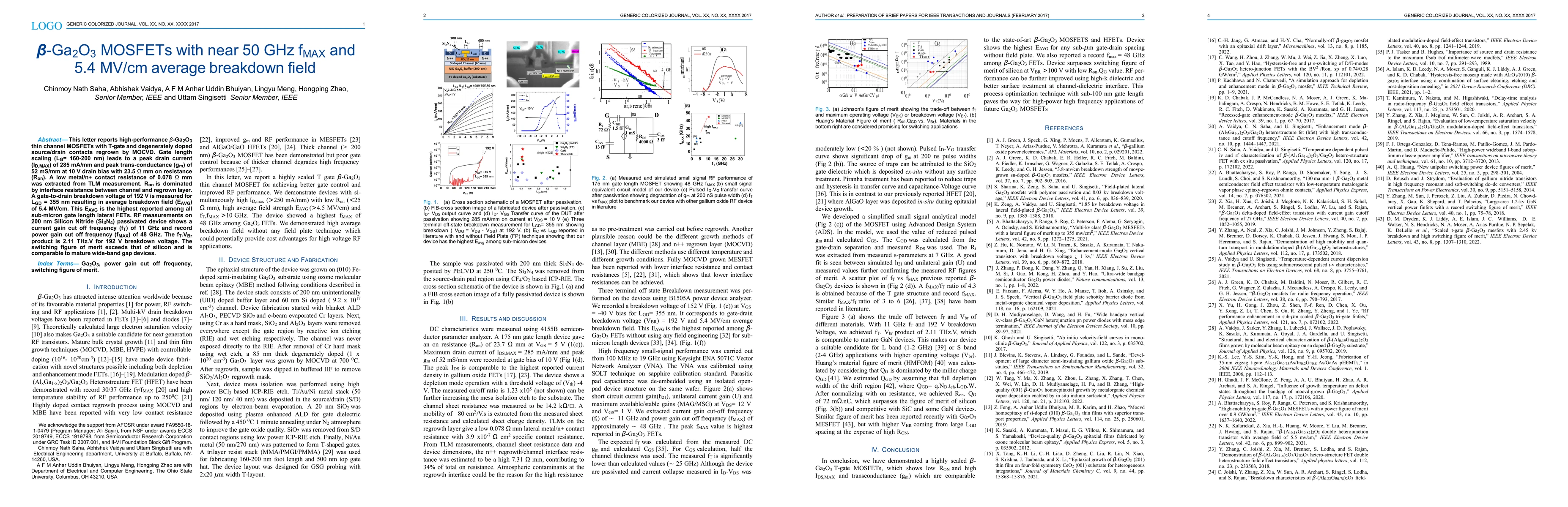
This letter reports high-performance $\mathrm{\beta} Ga2O3 thin channel MOSFETs with T-gate and degenerately doped source/drain contacts regrown by MOCVD. Gate length scaling (LG= 160-200 nm) leads ...

Thumbnail for MOCVD growth and band offsets of \k{appa}-phase Ga2O3 on sapphire, GaN,
  AlN and YSZ substrates
arXiv
MOCVD growth and band offsets of \k{appa}-phase Ga2O3 on sapphire, GaN, AlN and YSZ substrates

Epitaxial growth of \k{appa}-phase Ga2O3 thin films are investigated on c-plane sapphire, GaN- and AlNon-sapphire, and (100) oriented yttria stabilized zirconia (YSZ) substrates via metalorganic che...

Thumbnail for Large-Size Free-Standing Single-crystal b-Ga2O3 Membranes Fabricated by
  Hydrogen Implantation and Lift-Off
arXiv
Large-Size Free-Standing Single-crystal b-Ga2O3 Membranes Fabricated by Hydrogen Implantation and Lift-Off

In this paper, we have demonstrated the large-size free-standing single-crystal b-Ga2O3 NMs fabricated by the hydrogen implantation and lift-off process directly from MOCVD grown b-Ga2O3 epifilms on...

Thumbnail for Direct observation of site-specific dopant substitution in Si doped
  (AlxGa1-x)2O3 via Atom Probe Tomography
arXiv
Direct observation of site-specific dopant substitution in Si doped (AlxGa1-x)2O3 via Atom Probe Tomography

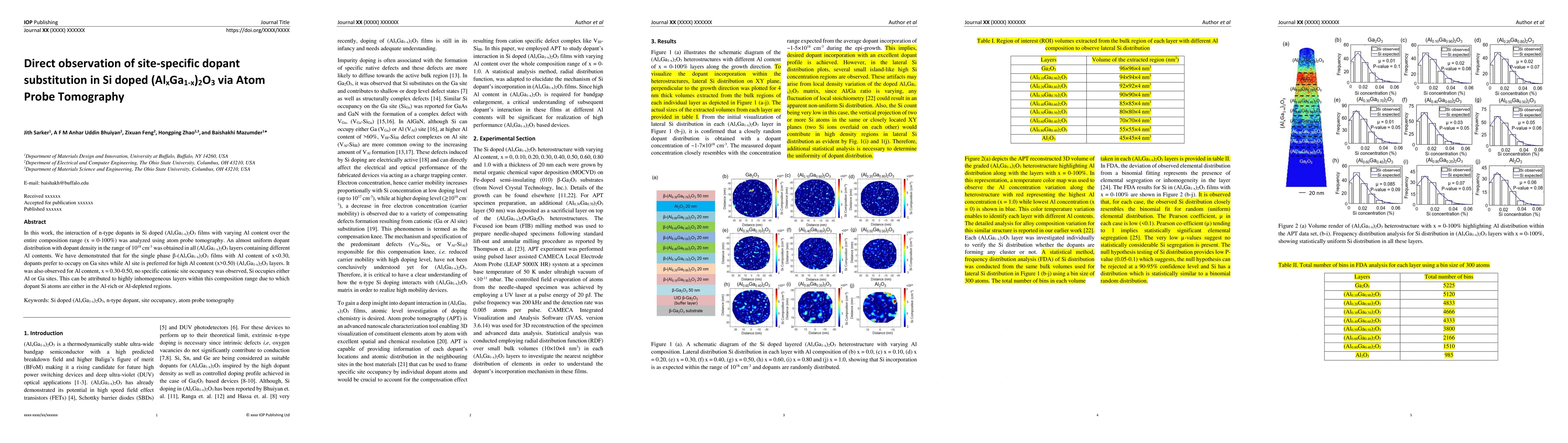
In this work, the interaction of n-type dopants in Si doped (AlxGa1-x)2O3 films with varying Al content over the entire composition range (x = 0-100%) was analyzed using atom probe tomography. An al...

Thumbnail for Electrostatic Engineering using Extreme Permittivity Materials for
  Ultra-wide Bandgap Semiconductor Transistors
arXiv
Electrostatic Engineering using Extreme Permittivity Materials for Ultra-wide Bandgap Semiconductor Transistors

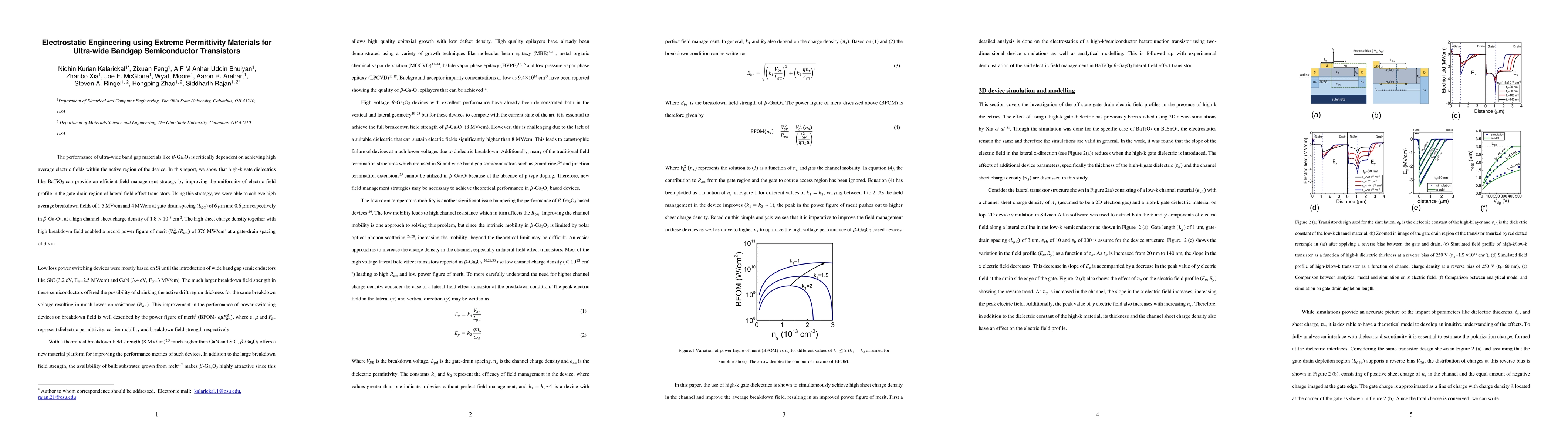
The performance of ultra-wide band gap materials like $\beta$-Ga$_\mathrm{2}$O$_\mathrm{3}$ is critically dependent on achieving high average electric fields within the active region of the device. ...

Thumbnail for Probing charge transport and background doping in MOCVD grown (010)
  ${\beta}$-Ga$_{2}$O$_{3}$
arXiv
Probing charge transport and background doping in MOCVD grown (010) ${\beta}$-Ga$_{2}$O$_{3}$

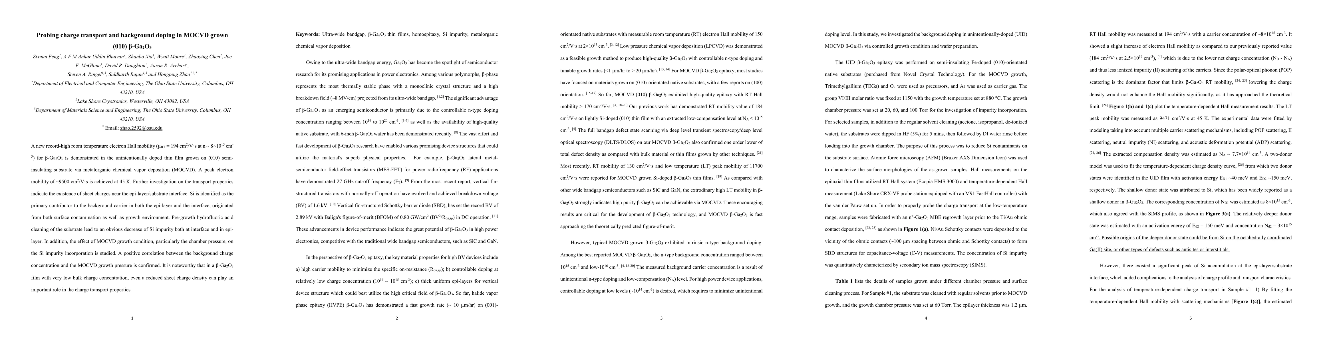
A new record-high room temperature electron Hall mobility (${\mu}_{RT} = 194\space cm^{2}/V\space s$ at $n\sim 8\times 10^{15}\space cm^{-3}$) for ${\beta}$-Ga2O3 is demonstrated in the unintentiona...

Thumbnail for LPCVD Grown Si-Doped $β$-Ga$_2$O$_3$ Films with Promising Electron
  Mobilities
arXiv
LPCVD Grown Si-Doped $β$-Ga$_2$O$_3$ Films with Promising Electron Mobilities

We systematically investigated the growth of Si-doped $\beta$-Ga$_2$O$_3$ films using LPCVD system, achieving high electron mobilities of 162 cm$^2$/V.s and 149 cm$^2$/V.s at carrier concentrations of...

Thumbnail for Radiation Resilience of $β$-Ga$_2$O$_3$ Schottky Barrier Diodes
  Under High Dose Gamma Radiation
arXiv
Radiation Resilience of $β$-Ga$_2$O$_3$ Schottky Barrier Diodes Under High Dose Gamma Radiation

A systematic investigation of the electrical characteristics of $\beta$-Ga$_2$O$_3$ Schottky barrier diodes (SBDs) has been conducted under high dose $^{60}$Co gamma radiation up to 5 Mrad (Si). Initi...

Thumbnail for Thermal Annealing and Radiation Effects on Structural and Electrical
  Properties of NbN/GaN Superconductor/Semiconductor Junctions
arXiv
Thermal Annealing and Radiation Effects on Structural and Electrical Properties of NbN/GaN Superconductor/Semiconductor Junctions

In the rapidly evolving field of quantum computing, niobium nitride (NbN) superconductors have emerged as integral components due to their unique structural properties, including a high superconductin...

Thumbnail for Electrical and Structural Properties of In-Situ MOCVD Grown
  Al$_2$O$_3$/$β$-Ga$_2$O$_3$ and
  Al$_2$O$_3$/$β$-(Al$_x$Ga$_{1-x}$)$_2$O$_3$ MOSCAPs
arXiv
Electrical and Structural Properties of In-Situ MOCVD Grown Al$_2$O$_3$/$β$-Ga$_2$O$_3$ and Al$_2$O$_3$/$β$-(Al$_x$Ga$_{1-x}$)$_2$O$_3$ MOSCAPs

This study investigates the electrical and structural properties of MOSCAPs with in-situ MOCVD-grown Al$_2$O$_3$ dielectrics on (010) $\beta$-Ga$_2$O$_3$ and $\beta$-(Al$_x$Ga$_{1-x}$)$_2$O$_3$ films....

Thumbnail for LPCVD based Plasma Damage Free in situ etching of $β$-Ga$_2$O$_3$
  using Solid Source Gallium
arXiv
LPCVD based Plasma Damage Free in situ etching of $β$-Ga$_2$O$_3$ using Solid Source Gallium

This work demonstrates a novel in situ etching technique for $\beta$-Ga$_2$O$_3$ using solid-source metallic Ga in a LPCVD system, enabling clean, anisotropic, plasma damage-free etching. Etching beha...

Thumbnail for Quasi-Vertical $β$-Ga$_2$O$_3$ Schottky Diodes on Sapphire Using
  All-LPCVD Growth and Plasma-Free Ga-Assisted Etching
arXiv
Quasi-Vertical $β$-Ga$_2$O$_3$ Schottky Diodes on Sapphire Using All-LPCVD Growth and Plasma-Free Ga-Assisted Etching

This work demonstrates quasi-vertical beta-Ga2O3 Schottky barrier diodes (SBDs) fabricated on c-plane sapphire using an all-LPCVD, plasma-free process integrating epitaxial growth of high-quality beta...

Thumbnail for Enhanced Breakdown Voltage in $β$-Ga$_2$O$_3$ Schottky Barrier
  Diodes via Fast Neutron Irradiation and Electrothermal Annealing
arXiv
Enhanced Breakdown Voltage in $β$-Ga$_2$O$_3$ Schottky Barrier Diodes via Fast Neutron Irradiation and Electrothermal Annealing

This study investigates the impact of fast neutron irradiation and post-radiation electro-thermal annealing on the electrical performance of $\beta$-Ga$_2$O$_3$ Schottky barrier diodes. Devices irradi...

Thumbnail for High-Purity Diamond Integration on $β$-Ga$_2$O$_3$ via Microwave Plasma CVD for Enhanced Thermal Management
arXiv
High-Purity Diamond Integration on $β$-Ga$_2$O$_3$ via Microwave Plasma CVD for Enhanced Thermal Management

The integration of diamond with $β$-Ga$_2$O$_3$ presents a promising pathway to enhance thermal management in high-power electronic devices, where the inherently low thermal conductivity of $β$-Ga$_2$...

This website uses cookies to ensure you get the best experience. Learn more