ArxivLens
A
Researcher

Abdelkarim Ouerghi

22 papers on arXiv

22 arXiv Papers
2 Total Publications
Profile

Academic Profile

Name A. Ouerghi
Total Papers 2
Scholar Profile View on Semantic Scholar
Metrics

Statistics

22 arXiv Papers
2 Total Publications
Publications

Papers on arXiv

Thumbnail for Magnetic evolution of Cr$_2$Te$_3$ epitaxially grown on graphene with
  post-growth annealing
arXiv
Magnetic evolution of Cr$_2$Te$_3$ epitaxially grown on graphene with post-growth annealing

Two-dimensional and van der Waals ferromagnets are ideal platform to study low dimensional magnetism and proximity effects in van der Waals heterostructures. Their ultimate two dimensional character...

Thumbnail for High Strain Engineering of a Suspended WSSe Monolayer Membrane by
  Indentation and Measured by Tip-enhanced Photoluminescence
arXiv
High Strain Engineering of a Suspended WSSe Monolayer Membrane by Indentation and Measured by Tip-enhanced Photoluminescence

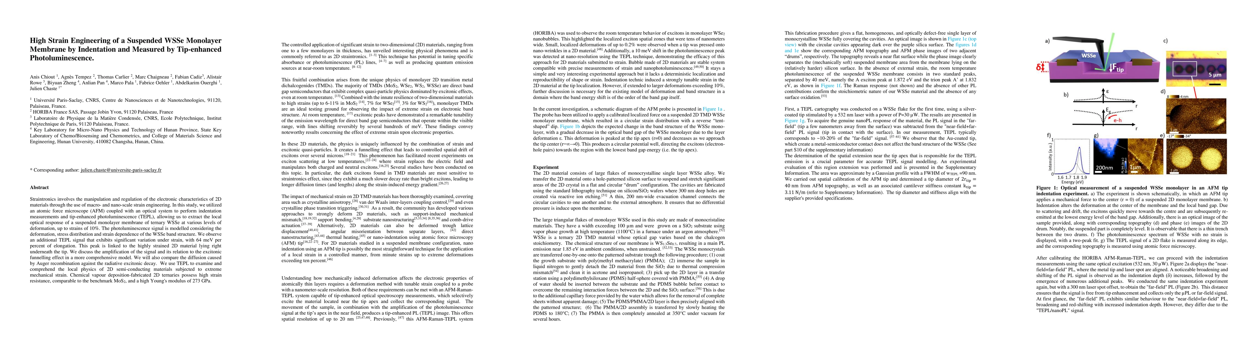
Straintronics involves the manipulation and regulation of the electronic characteristics of 2D materials through the use of macro- and nano-scale strain engineering. In this study, we utilized an at...

Thumbnail for Reconfigurable Multifunctional van der Waals Ferroelectric Devices and
  Logic Circuits
arXiv
Reconfigurable Multifunctional van der Waals Ferroelectric Devices and Logic Circuits

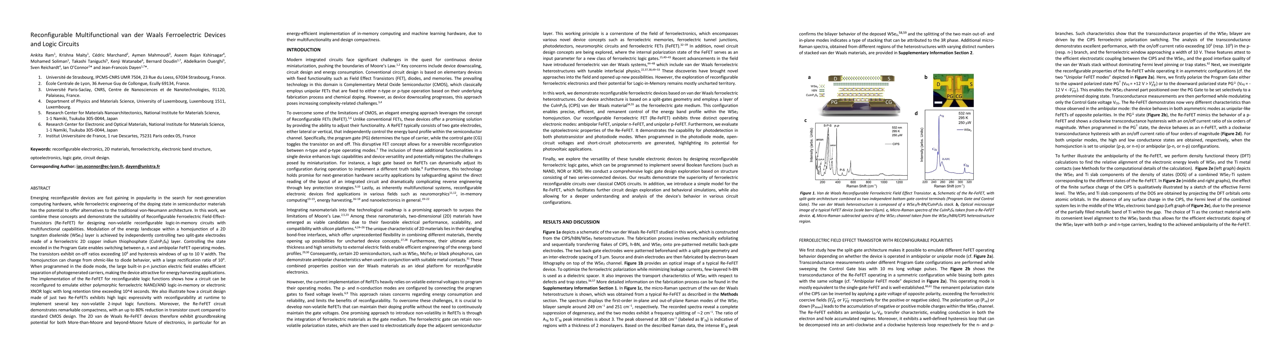
In this work, we demonstrate the suitability of Reconfigurable Ferroelectric Field-Effect- Transistors (Re-FeFET) for designing non-volatile reconfigurable logic-in-memory circuits with multifunctio...

Thumbnail for Quasi van der Waals Epitaxy of Rhombohedral-stacked Bilayer WSe2 on
  GaP(111) Heterostructure
arXiv
Quasi van der Waals Epitaxy of Rhombohedral-stacked Bilayer WSe2 on GaP(111) Heterostructure

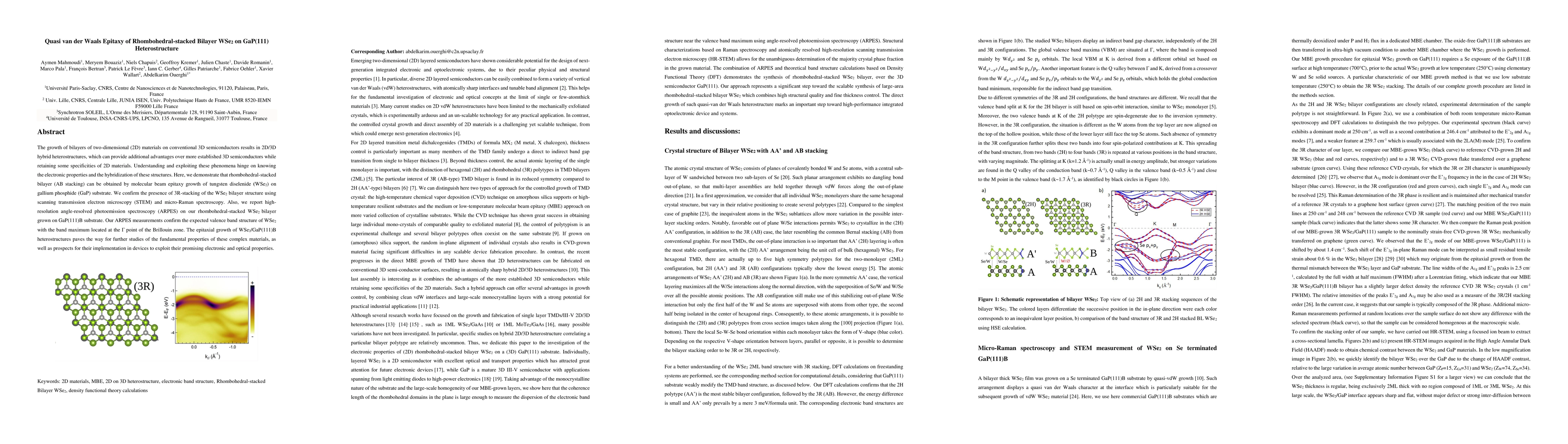
The growth of bilayers of two-dimensional (2D) materials on conventional 3D semiconductors results in 2D/3D hybrid heterostructures, which can provide additional advantages over more established 3D ...

Thumbnail for Intrinsic defects and mid-gap states in quasi-one-dimensional Indium
  Telluride
arXiv
Intrinsic defects and mid-gap states in quasi-one-dimensional Indium Telluride

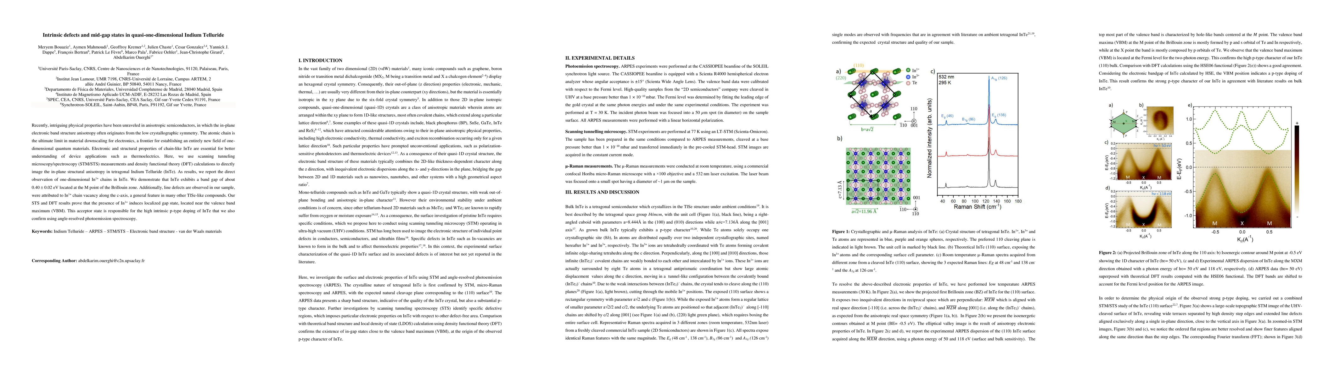
Recently, intriguing physical properties have been unraveled in anisotropic semiconductors, in which the in-plane electronic band structure anisotropy often originates from the low crystallographic ...

Thumbnail for Quantum Confinement and Electronic Structure at the Surface of van der
  Waals Ferroelectric {\alpha}-In$_{2}$Se$_{3}$
arXiv
Quantum Confinement and Electronic Structure at the Surface of van der Waals Ferroelectric {\alpha}-In$_{2}$Se$_{3}$

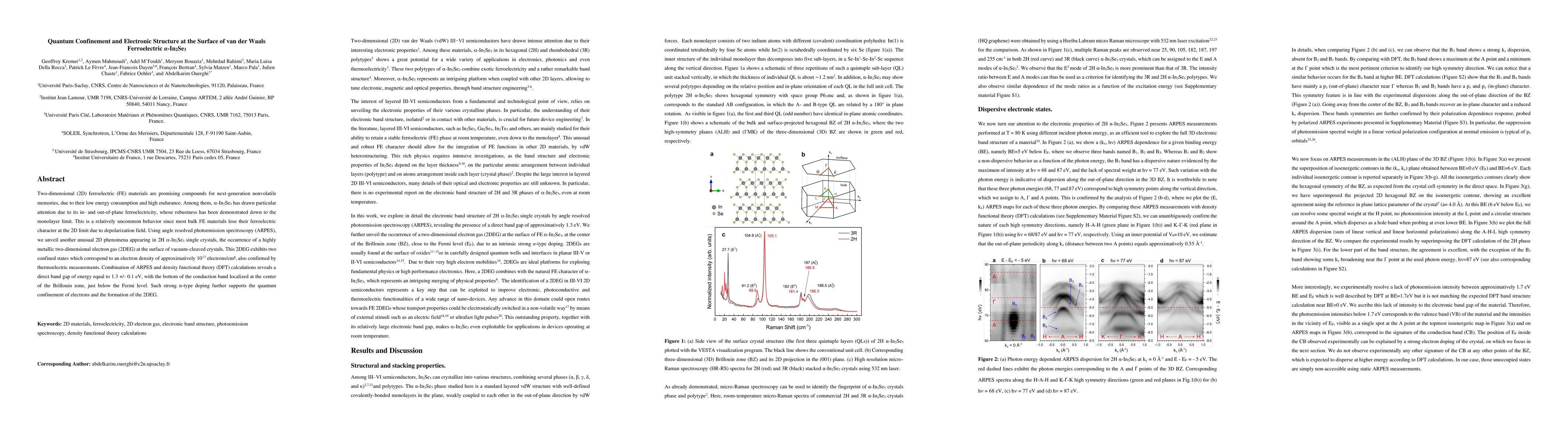
Two-dimensional (2D) ferroelectric (FE) materials are promising compounds for next-generation nonvolatile memories, due to their low energy consumption and high endurance. Among them, {\alpha}-In$_{...

Thumbnail for Hydrogenic Spin-Valley states of the Bromine donor in 2H-MoTe$_2$
arXiv
Hydrogenic Spin-Valley states of the Bromine donor in 2H-MoTe$_2$

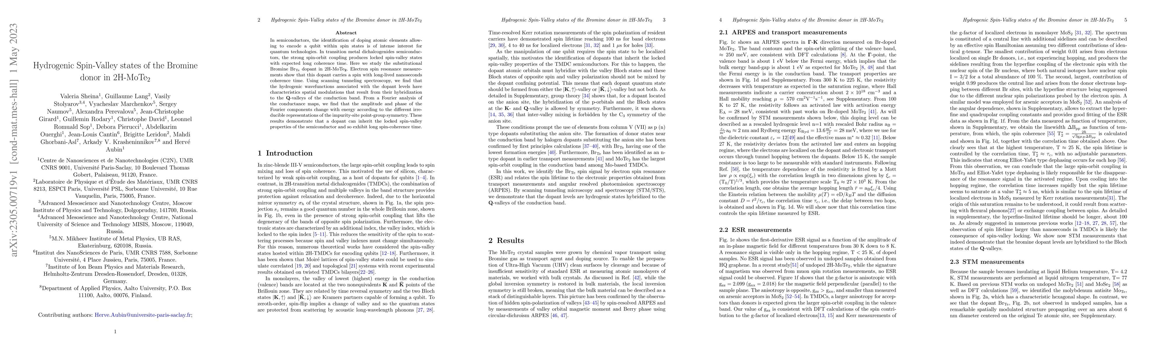
In semiconductors, the identification of doping atomic elements allowing to encode a qubit within spin states is of intense interest for quantum technologies. In transition metal dichalcogenides sem...

Thumbnail for Epitaxial van der Waals heterostructures of Cr2Te3 on 2D materials
arXiv
Epitaxial van der Waals heterostructures of Cr2Te3 on 2D materials

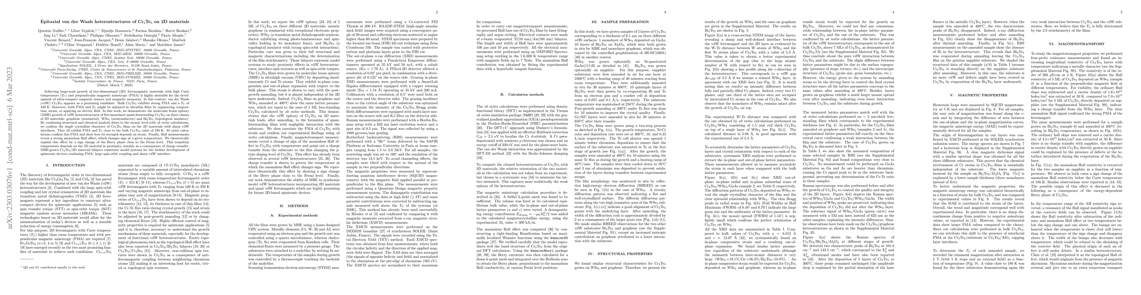
Achieving large-scale growth of two-dimensional (2D) ferromagnetic materials with high Curie temperature (TC) and perpendicular magnetic anisotropy (PMA) is highly desirable for the development of u...

Thumbnail for Unidirectional Rashba Spin Splitting in Single Layer
  WS$_{2(1-x)}$Se$_{2x}$ alloy
arXiv
Unidirectional Rashba Spin Splitting in Single Layer WS$_{2(1-x)}$Se$_{2x}$ alloy

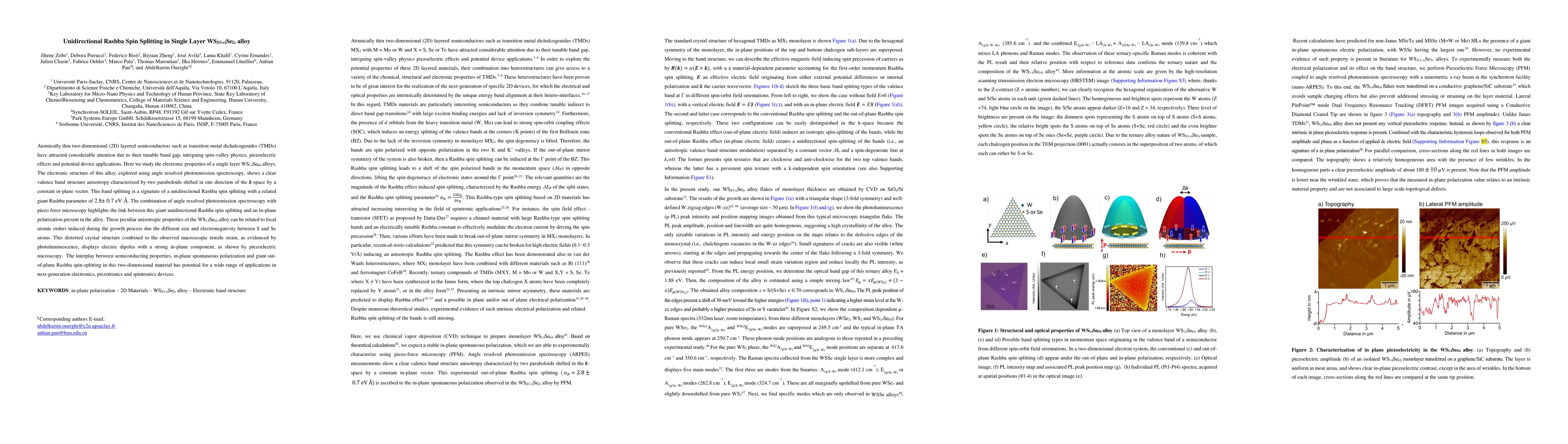
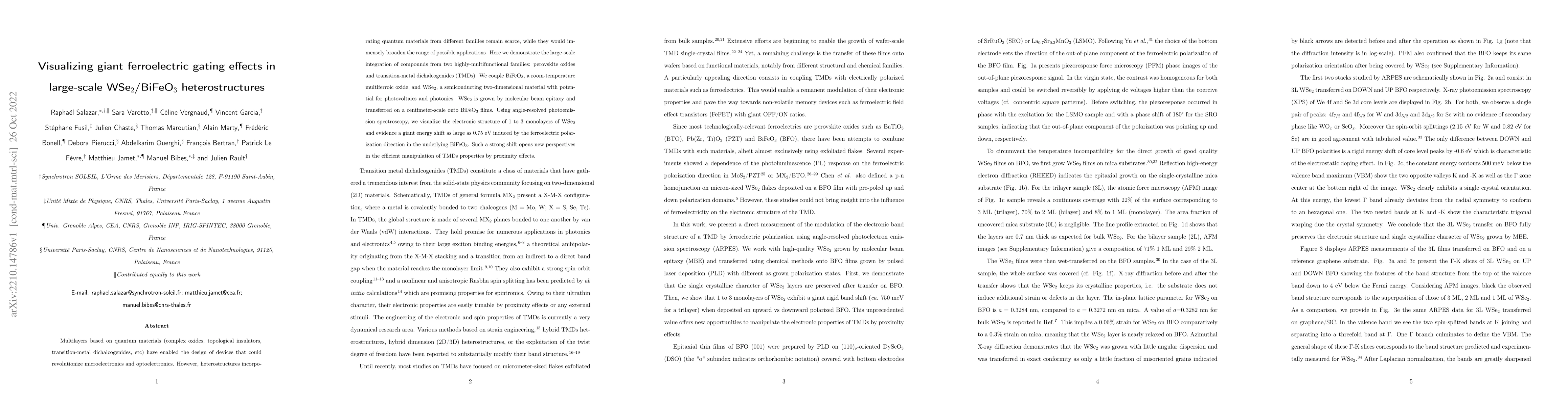
Atomically thin two-dimensional (2D) layered semiconductors such as transition metal dichalcogenides (TMDs) have attracted considerable attention due to their tunable band gap, intriguing spin-valle...

Thumbnail for Visualizing giant ferroelectric gating effects in large-scale
  WSe$_2$/BiFeO$_3$ heterostructures
arXiv
Visualizing giant ferroelectric gating effects in large-scale WSe$_2$/BiFeO$_3$ heterostructures

Multilayers based on quantum materials (complex oxides, topological insulators, transition-metal dichalcogenides, etc) have enabled the design of devices that could revolutionize microelectronics an...

Thumbnail for Electroluminescence of monolayer WS$_2$ in a scanning tunneling
  microscope: the effect of bias polarity on the spectral and angular
  distribution of the emitted light
arXiv
Electroluminescence of monolayer WS$_2$ in a scanning tunneling microscope: the effect of bias polarity on the spectral and angular distribution of the emitted light

Inelastic electron tunneling in a scanning tunneling microscope (STM) is used to generate excitons in monolayer tungsten disulfide (WS$_2$). Excitonic electroluminescence is measured both at positiv...

Thumbnail for Evidence for Highly p-type doping and type II band alignment in large
  scale monolayer WSe2 /Se-terminated GaAs heterojunction grown by Molecular
  beam epitaxy
arXiv
Evidence for Highly p-type doping and type II band alignment in large scale monolayer WSe2 /Se-terminated GaAs heterojunction grown by Molecular beam epitaxy

Two-dimensional materials (2D) arranged in hybrid van der Waals (vdW) heterostructures provide a route toward the assembly of 2D and conventional III-V semiconductors. Here, we report the structural...

Thumbnail for Hybridization and localized flat band in the WSe2/MoSe2 heterobilayer
  grown by molecular beam epitaxy
arXiv
Hybridization and localized flat band in the WSe2/MoSe2 heterobilayer grown by molecular beam epitaxy

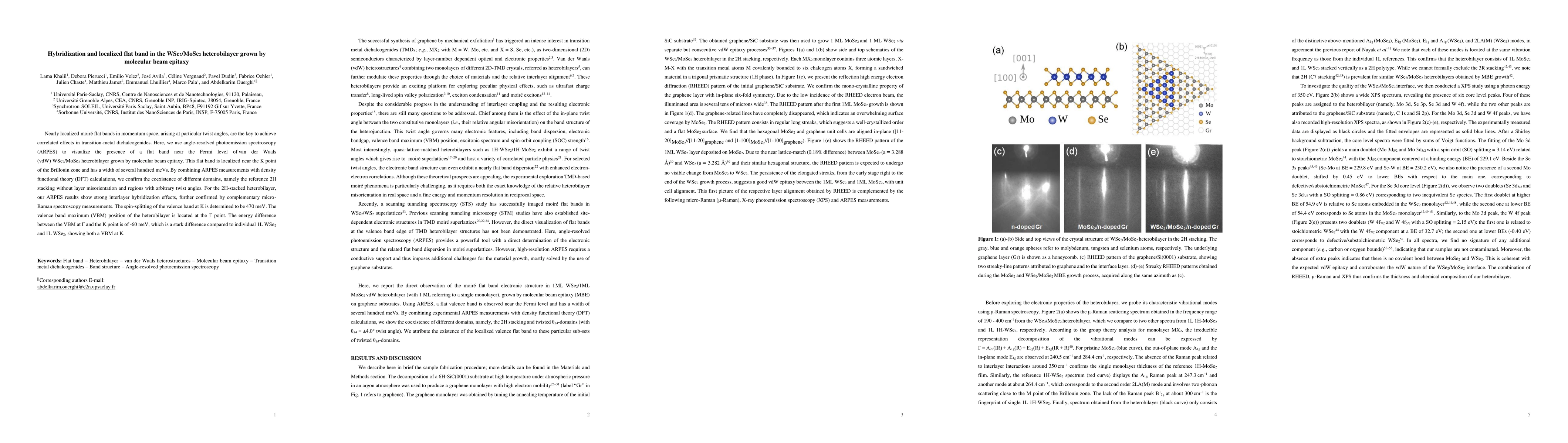
Nearly localized moire flat bands in momentum space, arising at particular twist angles, are the key to achieve correlated effects in transition-metal dichalcogenides. Here, we use angle-resolved ph...

Thumbnail for High carrier mobility in single-crystal PtSe2 grown by molecular beam
  epitaxy on ZnO(0001)
arXiv
High carrier mobility in single-crystal PtSe2 grown by molecular beam epitaxy on ZnO(0001)

PtSe2 is attracting considerable attention as a high mobility two-dimensional material with envisionned applications in microelectronics, photodetection and spintronics. The growth of high quality P...

Thumbnail for Indirect to direct band gap crossover in two-dimensional WS2(1-x)Se2x
  alloys
arXiv
Indirect to direct band gap crossover in two-dimensional WS2(1-x)Se2x alloys

In atomically thin transition metal dichalcogenide semiconductors, there is a crossover from indirect to direct bandgap as the thickness drops to one monolayer, which comes with a fast increase of t...

Thumbnail for Phase Transition in a Memristive Suspended MoS2 Monolayer Probed by
  Opto- and Electro-Mechanics
arXiv
Phase Transition in a Memristive Suspended MoS2 Monolayer Probed by Opto- and Electro-Mechanics

Semiconducting monolayer of 2D material are able to concatenate multiple interesting properties into a single component. Here, by combining opto-mechanical and electronic measurements, we demonstrat...

Thumbnail for Distinguishing different stackings in WSe2 bilayers grown Using Chemical
  Vapor Deposition
arXiv
Distinguishing different stackings in WSe2 bilayers grown Using Chemical Vapor Deposition

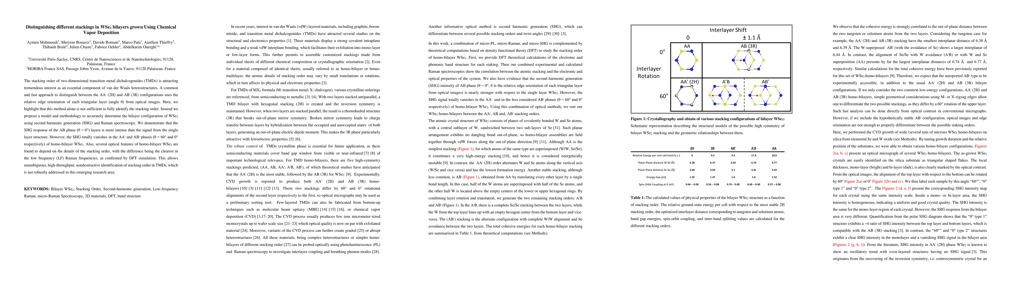
The stacking order of two-dimensional transition metal dichalcogenides (TMDs) is attracting tremendous interest as an essential component of van der Waals heterostructures. A common and fast approach ...

Thumbnail for Growth of Highly Conductive PtSe2 Films Controlled by Raman Metrics for
  High-Frequency Photodetectors and Optoelectronic Mixers at 1.55 μm
arXiv
Growth of Highly Conductive PtSe2 Films Controlled by Raman Metrics for High-Frequency Photodetectors and Optoelectronic Mixers at 1.55 μm

Two-dimensional PtSe2 exhibits outstanding intrinsic properties such as high carrier mobility, tunable bandgap, broadband absorption and air stability, making it ideal for (opto)electronic application...

Thumbnail for Mexican hat-like valence band dispersion and quantum confinement in
  rhombohedral ferroelectric alpha-In2Se3
arXiv
Mexican hat-like valence band dispersion and quantum confinement in rhombohedral ferroelectric alpha-In2Se3

Two-dimensional (2D) ferroelectric (FE) materials offer a large variety of electronic properties depending on chemical composition, number of layers and stacking-order. Among them, alpha-In2Se3 has at...

Thumbnail for Hybridization in van der Waals epitaxy of PtSe2/h-BN and PtSe2/graphene
  heterostructures
arXiv
Hybridization in van der Waals epitaxy of PtSe2/h-BN and PtSe2/graphene heterostructures

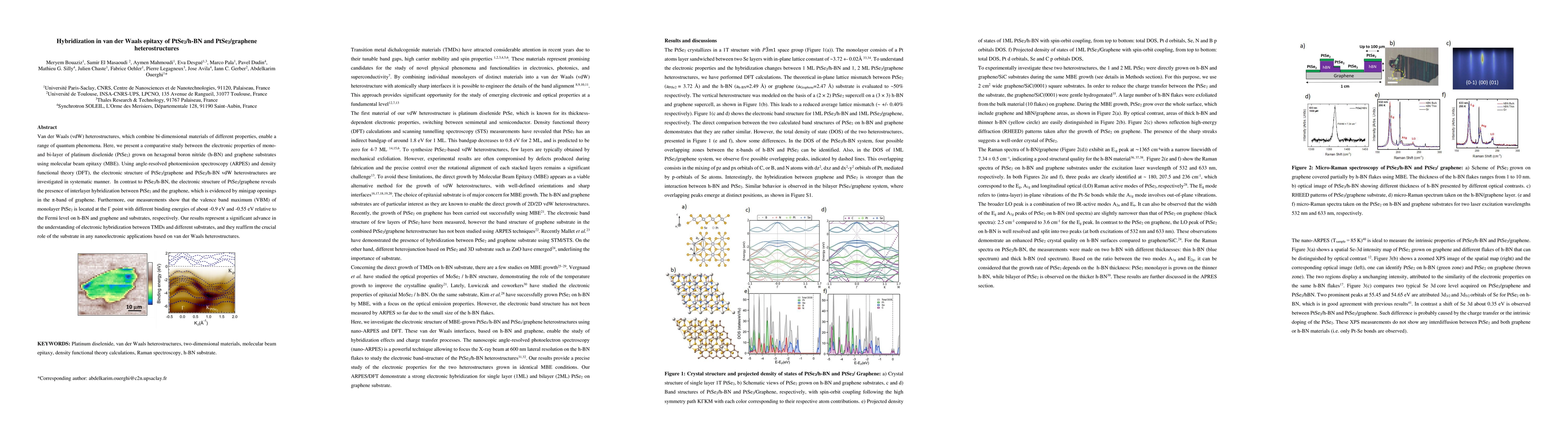
Van der Waals (vdW) heterostructures, which combine bi-dimensional materials of different properties, enable a range of quantum phenomena. Here, we present a comparative study between the electronic p...

Thumbnail for Tunable electronic band structure in WSSe van der Waals Alloys
arXiv
Tunable electronic band structure in WSSe van der Waals Alloys

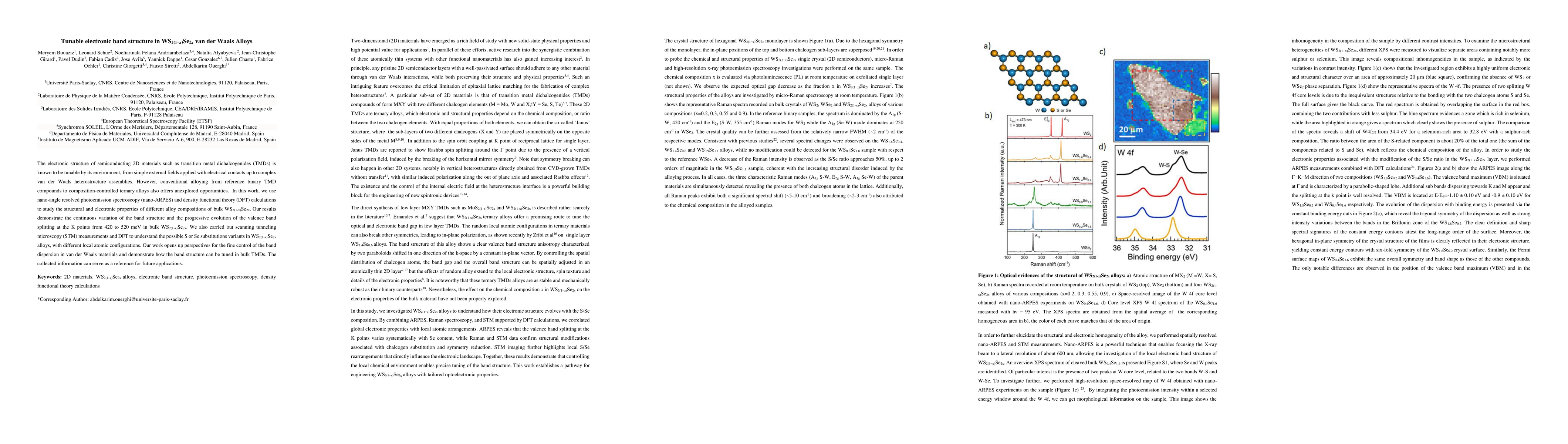
The electronic structure of semiconducting 2D materials such as transition metal dichalcogenides (TMDs) is known to be tunable by its environment, from simple external fields applied with electrical c...

Thumbnail for Epitaxial Growth and Electronic Properties of QuasiFreeStanding Rhombohedral WSe2 Bilayers on Cubic W110
arXiv
Epitaxial Growth and Electronic Properties of QuasiFreeStanding Rhombohedral WSe2 Bilayers on Cubic W110

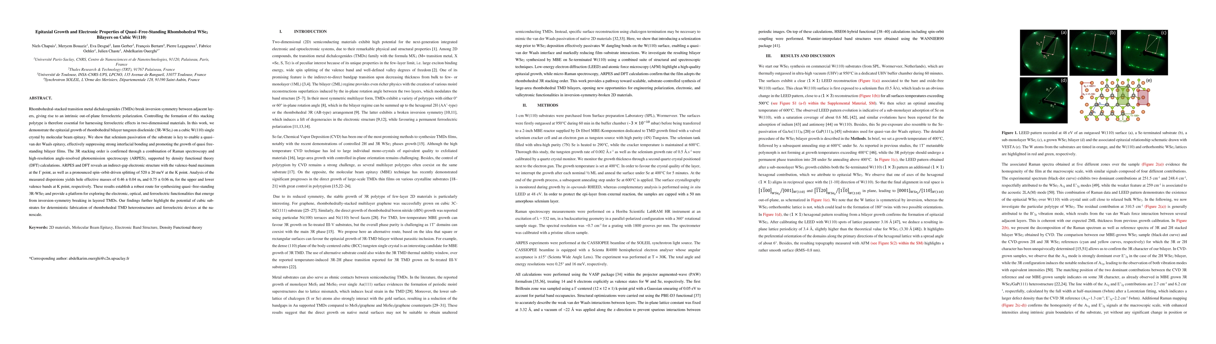
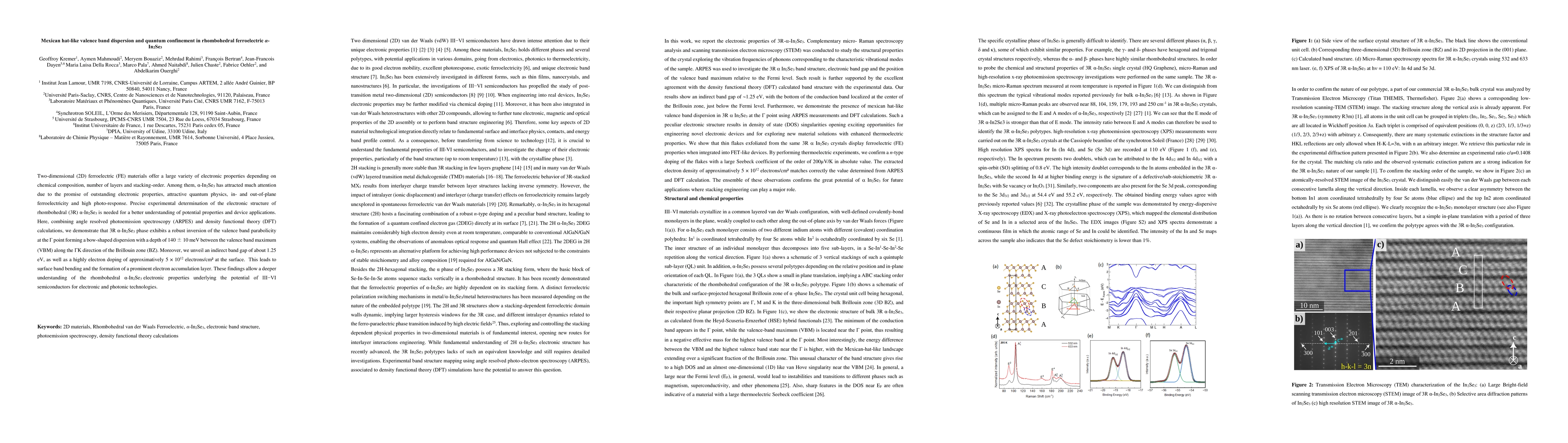
Rhombohedral-stacked transition metal dichalcogenides (TMDs) break inversion symmetry between adjacent layers, giving rise to an intrinsic out-of-plane ferroelectric polarization.Controlling the forma...

This website uses cookies to ensure you get the best experience. Learn more