ArxivLens
A
Researcher

Abin Varghese

8 papers on arXiv

8 arXiv Papers
2 Total Publications
Profile

Academic Profile

Name A. Varghese
Total Papers 2
Scholar Profile View on Semantic Scholar
Metrics

Statistics

8 arXiv Papers
2 Total Publications
Publications

Papers on arXiv

Thumbnail for An electroplating-based plasmonic platform for giant emission
  enhancement in monolayer semiconductors
arXiv
An electroplating-based plasmonic platform for giant emission enhancement in monolayer semiconductors

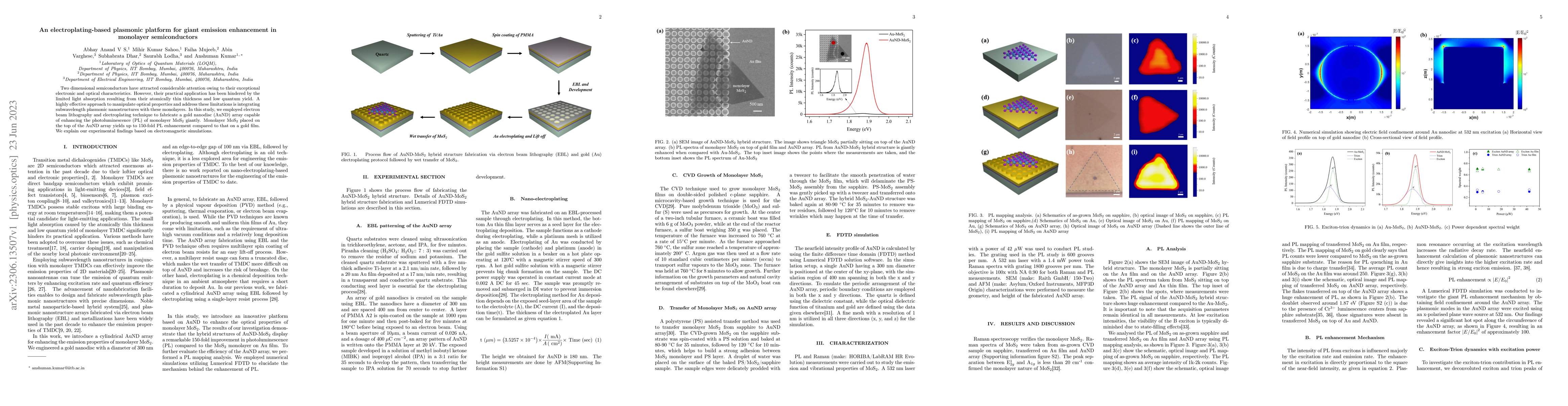
Two dimensional semiconductors have attracted considerable attention owing to their exceptional electronic and optical characteristics. However, their practical application has been hindered by the ...

Thumbnail for Electrically Controlled Reversible Strain Modulation in MoS$_2$
  Field-effect Transistors via an Electro-mechanically Coupled Piezoelectric
  Thin Film
arXiv
Electrically Controlled Reversible Strain Modulation in MoS$_2$ Field-effect Transistors via an Electro-mechanically Coupled Piezoelectric Thin Film

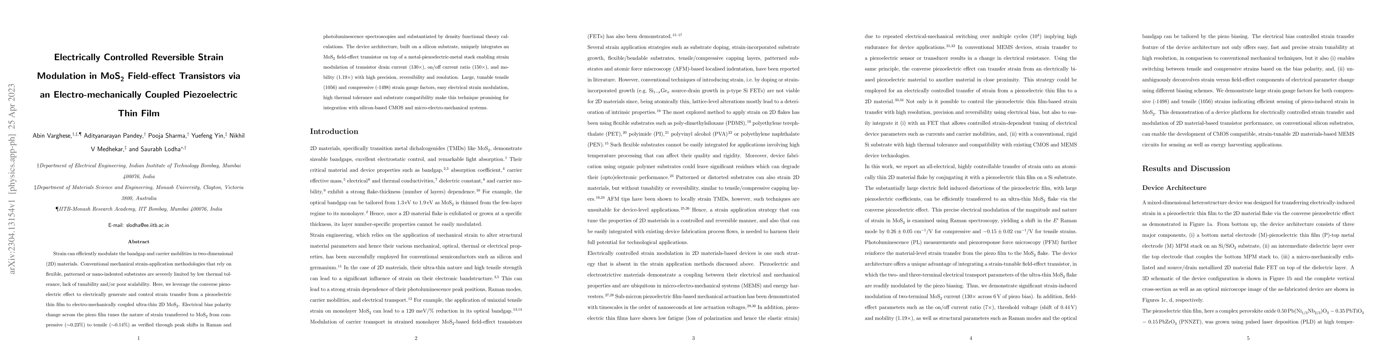
Strain can efficiently modulate the bandgap and carrier mobilities in two-dimensional (2D) materials. Conventional mechanical strain-application methodologies that rely on flexible, patterned or nan...

Thumbnail for Wavelength-Controlled Photocurrent Polarity Switching in BP-MoS$_2$
  Heterostructure
arXiv
Wavelength-Controlled Photocurrent Polarity Switching in BP-MoS$_2$ Heterostructure

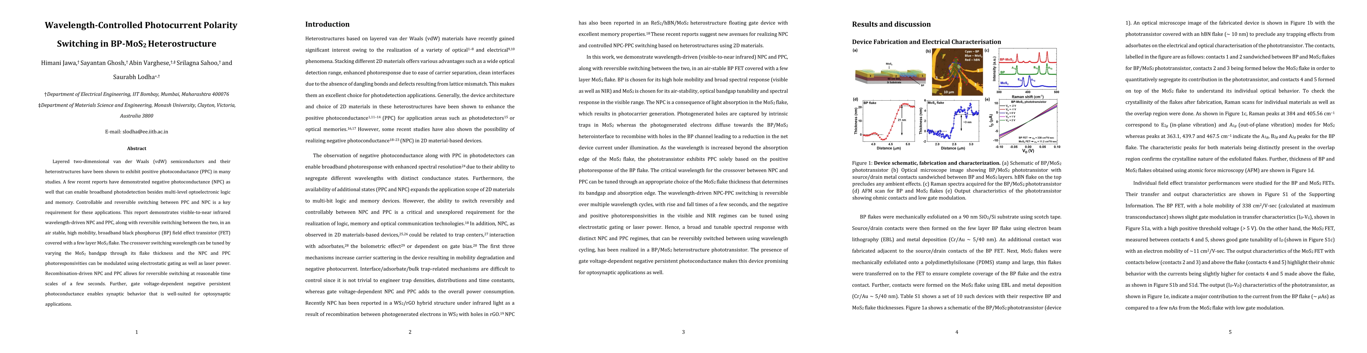
Layered two-dimensional van der Waals (vdW) semiconductors and their heterostructures have been shown to exhibit positive photoconductance (PPC) in many studies. A few recent reports have demonstrat...

Thumbnail for Near-Infrared and Visible-range Optoelectronics in 2D Hybrid
  Perovskite/Transition Metal Dichalcogenide Heterostructures
arXiv
Near-Infrared and Visible-range Optoelectronics in 2D Hybrid Perovskite/Transition Metal Dichalcogenide Heterostructures

The application of ultrathin two-dimensional (2D) perovskites in near-infrared and visible-range optoelectronics has been limited owing to their inherent wide bandgaps, large excitonic binding energ...

Thumbnail for Enhanced gas sensing performance and all-electrical room temperature
  operation enabled by a WSe2/MoS2 heterojunction
arXiv
Enhanced gas sensing performance and all-electrical room temperature operation enabled by a WSe2/MoS2 heterojunction

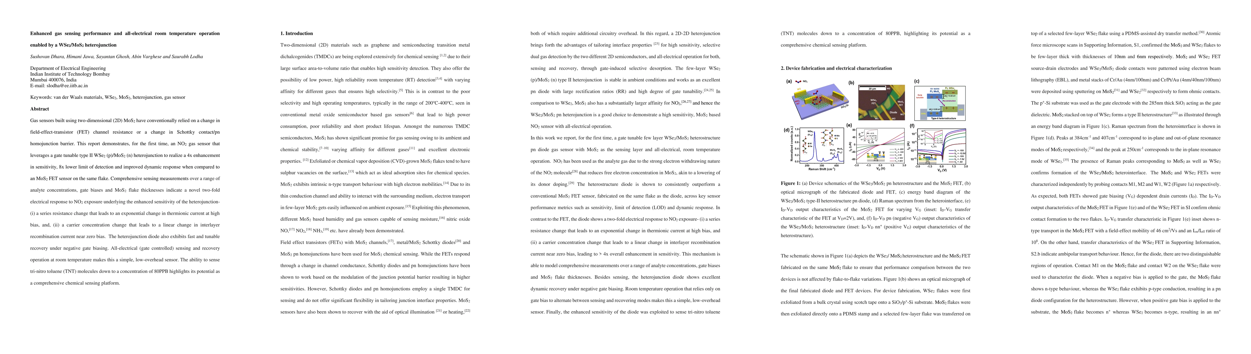
Gas sensors built using two-dimensional (2D) MoS2 have conventionally relied on a change in field-effect-transistor (FET) channel resistance or a change in Schottky contact/pn homojunction barrier. ...

Thumbnail for Electrically Tunable Room Temperature Hysteresis Crossover in Underlap
  MoS$_2$ FETs
arXiv
Electrically Tunable Room Temperature Hysteresis Crossover in Underlap MoS$_2$ FETs

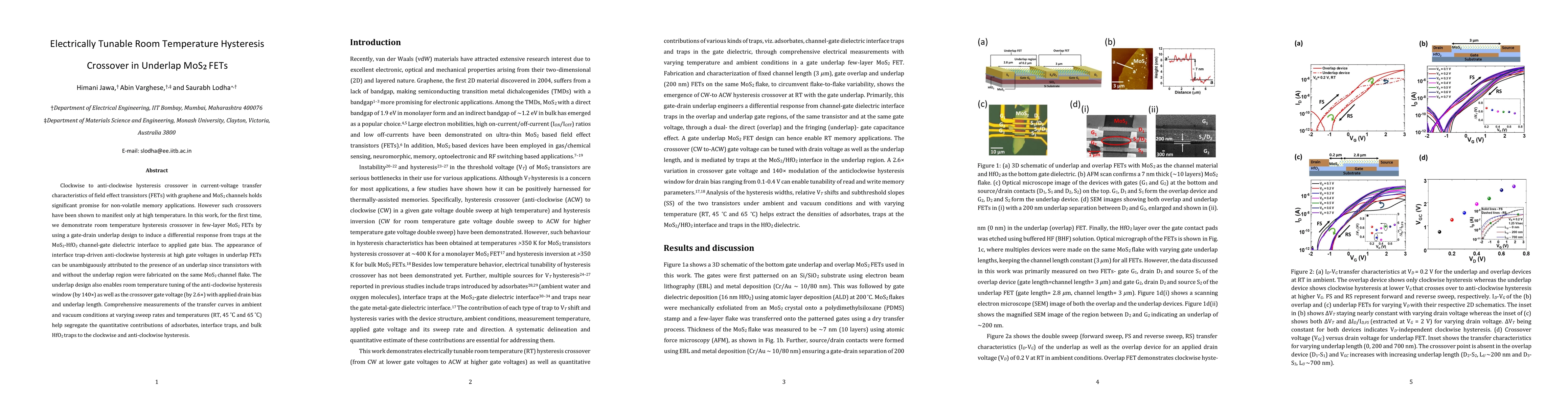
Clockwise to anti-clockwise hysteresis crossover in current-voltage transfer characteristics of field effect transistors (FETs) with graphene and MoS$_2$ channels holds significant promise for non-v...

Thumbnail for Near-direct bandgap $WSe_2$/$ReS_2$ type-II pn heterojunction for
  enhanced ultrafast photodetection and high-performance photovoltaics
arXiv
Near-direct bandgap $WSe_2$/$ReS_2$ type-II pn heterojunction for enhanced ultrafast photodetection and high-performance photovoltaics

PN heterojunctions comprising layered van der Waals (vdW) semiconductors have been used to demonstrate current rectifiers, photodetectors, and photovoltaic devices. However, a direct or near-direct ...

Thumbnail for Vertically Integrated Dual-memtransistor Enabled Reconfigurable
  Heterosynaptic Sensorimotor Networks and In-memory Neuromorphic Computing
arXiv
Vertically Integrated Dual-memtransistor Enabled Reconfigurable Heterosynaptic Sensorimotor Networks and In-memory Neuromorphic Computing

Neuromorphic in-memory computing requires area-efficient architecture for seamless and low latency parallel processing of large volumes of data. Here, we report a compact, vertically integrated/strati...

This website uses cookies to ensure you get the best experience. Learn more