Adam Charnas

6 papers on arXiv

Academic Profile

Name: A. Charnas
Total Papers: 50

Statistics

arXiv Papers 6
Total Publications 50

Papers on arXiv

Thumbnail for A Gate-All-Around Single-Channel In2O3 Nanoribbon FET with Near 20
  mA/{\mu}m Drain Current

A Gate-All-Around Single-Channel In2O3 Nanoribbon FET with Near 20 mA/{\mu}m Drain Current

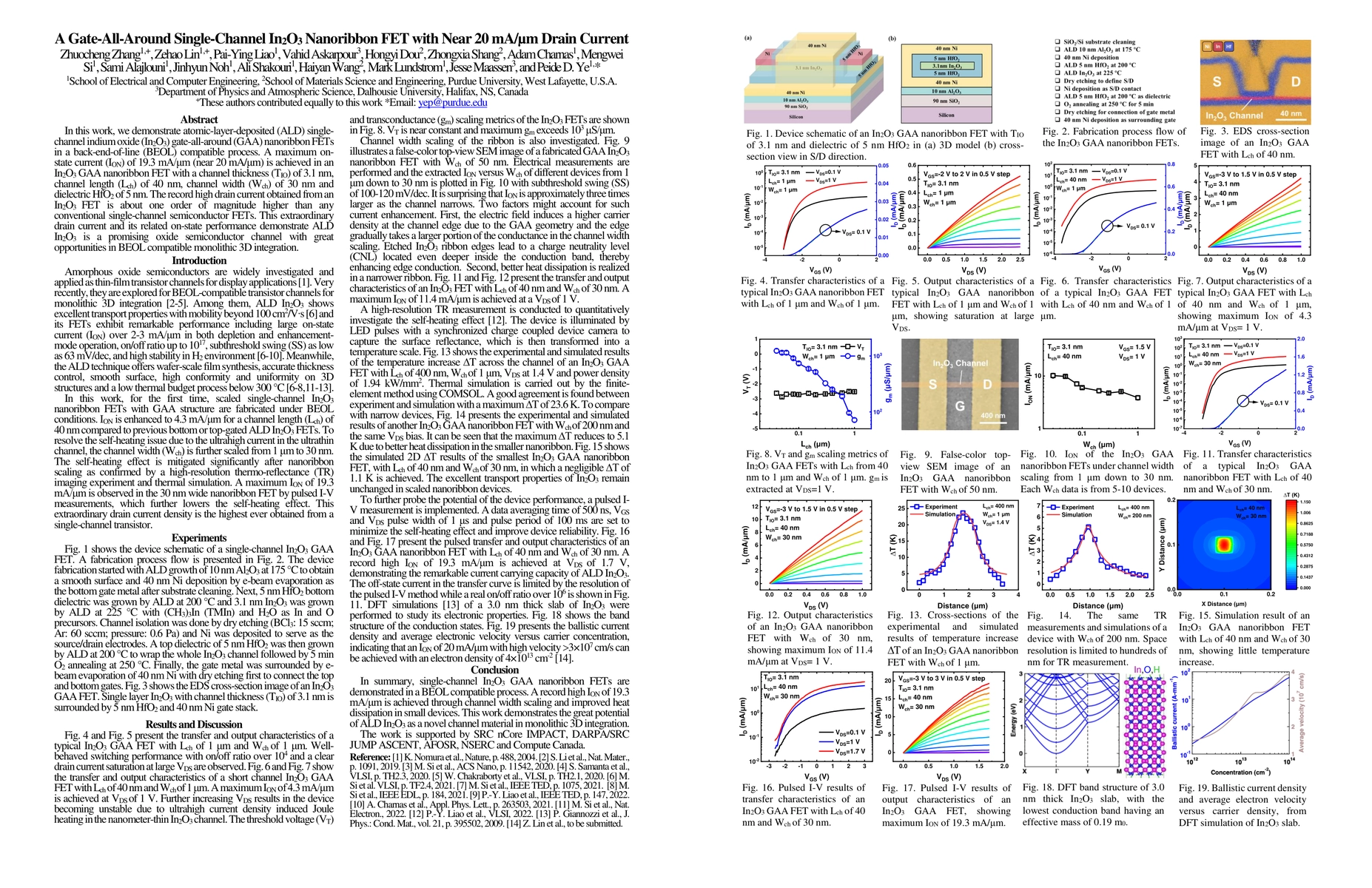
In this work, we demonstrate atomic-layer-deposited (ALD) single-channel indium oxide (In2O3) gate-all-around (GAA) nanoribbon FETs in a back-end-of-line (BEOL) compatible process. A maximum on-stat...

Thumbnail for A Nanometer-Thick Oxide Semiconductor Transistor with Ultra-High Drain
  Current

A Nanometer-Thick Oxide Semiconductor Transistor with Ultra-High Drain Current

High drive current is a critical performance parameter in semiconductor devices for high-speed, low-power logic applications or high-efficiency, high-power, high-speed radio frequency (RF) analog ap...

Thumbnail for Why In2O3 Can Make 0.7 nm Atomic Layer Thin Transistors?

Why In2O3 Can Make 0.7 nm Atomic Layer Thin Transistors?

In this work, we demonstrate enhancement-mode field-effect transistors by atomic-layer-deposited (ALD) amorphous In2O3 channel with thickness down to 0.7 nm. Thickness is found to be critical on the...

Thumbnail for Scaled Atomic-Layer-Deposited Indium Oxide Nanometer Transistors with
  Maximum Drain Current Exceeding 2 A/mm at Drain Voltage of 0.7 V

Scaled Atomic-Layer-Deposited Indium Oxide Nanometer Transistors with Maximum Drain Current Exceeding 2 A/mm at Drain Voltage of 0.7 V

In this work, we demonstrate scaled back-end-of-line (BEOL) compatible indium oxide (In2O3) transistors by atomic layer deposition (ALD) with channel thickness (Tch) of 1.0-1.5 nm, channel length (L...

Thumbnail for Raman Response and Transport Properties of One-Dimensional van der Waals
  Tellurium Nanowires

Raman Response and Transport Properties of One-Dimensional van der Waals Tellurium Nanowires

Tellurium can form nanowires of helical atomic chains. Given their unique one-dimensional van der Waals structure, these nanowires are expected to show remarkably different physical and electronic p...

Thumbnail for Breakdown of Ohm's Law by Disorders in Low-Dimensional Transistors

Breakdown of Ohm's Law by Disorders in Low-Dimensional Transistors

Ohm's law provides a fundamental framework for understanding charge transport in conductors and underpins the concept of electrical scaling that has enabled the continuous advancement of modern CMOS t...

This website uses cookies to ensure you get the best experience. Learn more