Academic Profile
Statistics
Similar Authors
Papers on arXiv
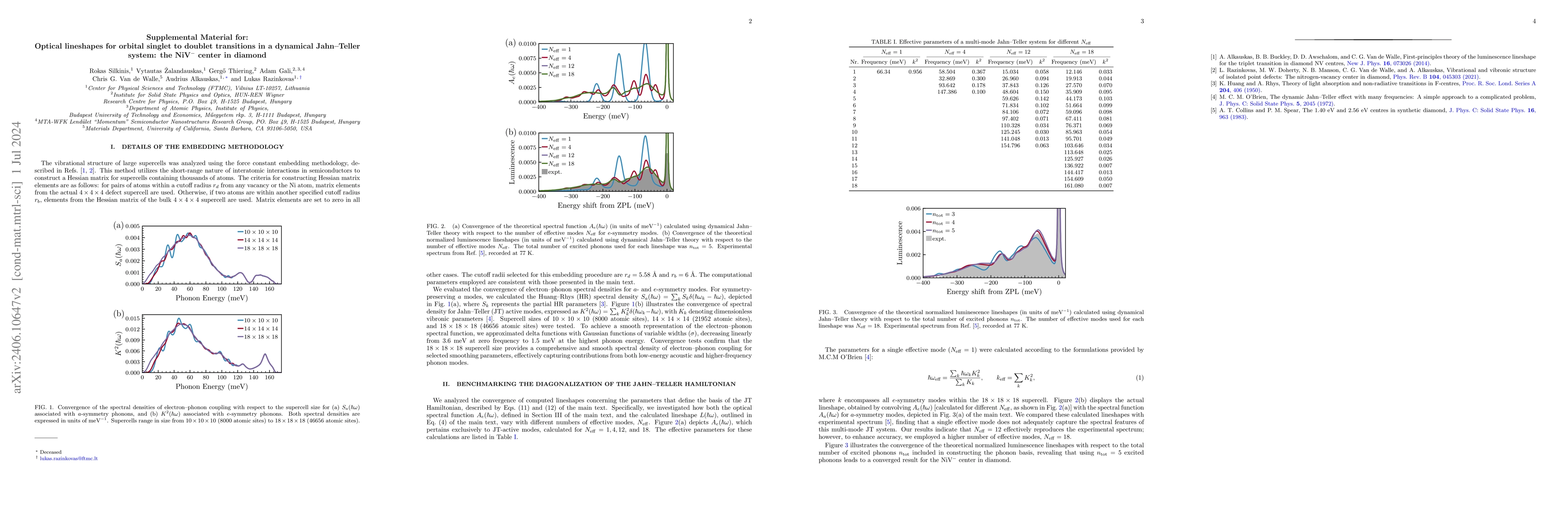
We apply density functional theory to investigate interactions between electronic and vibrational states in crystal defects with multi-mode dynamical Jahn-Teller (JT) systems. Our focus is on transi...
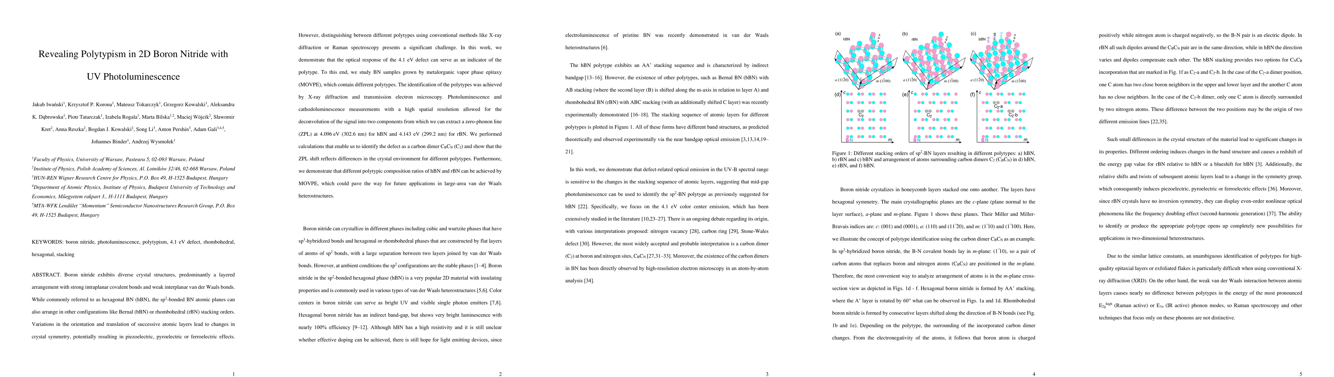
Boron nitride exhibits diverse crystal structures, predominantly a layered arrangement with strong intraplanar covalent bonds and weak interplanar van der Waals bonds. While commonly referred to as ...
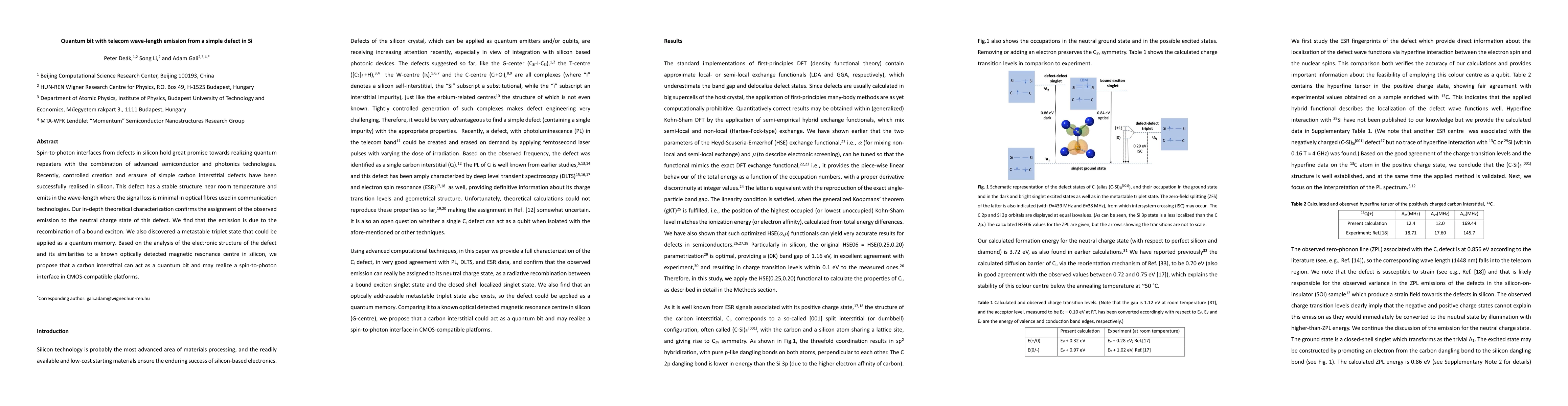
Spin-to-photon interfaces from defects in silicon hold great promise towards realizing quantum repeaters with the combination of advanced semiconductor and photonics technologies. Recently, controll...
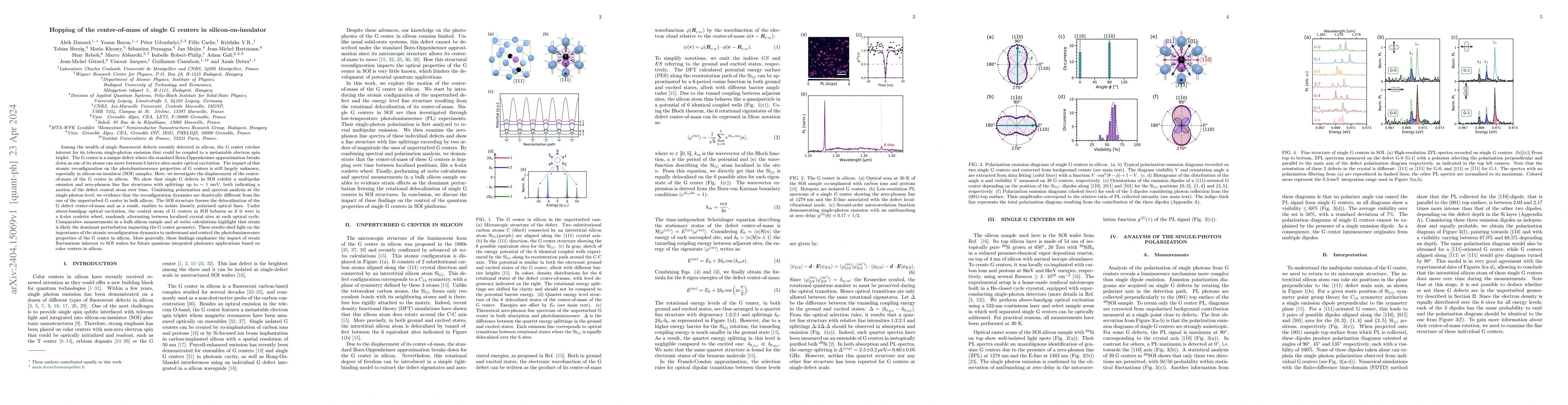
Among the wealth of single fluorescent defects recently detected in silicon, the G center catches interest for its telecom single-photon emission that could be coupled to a metastable electron spin ...
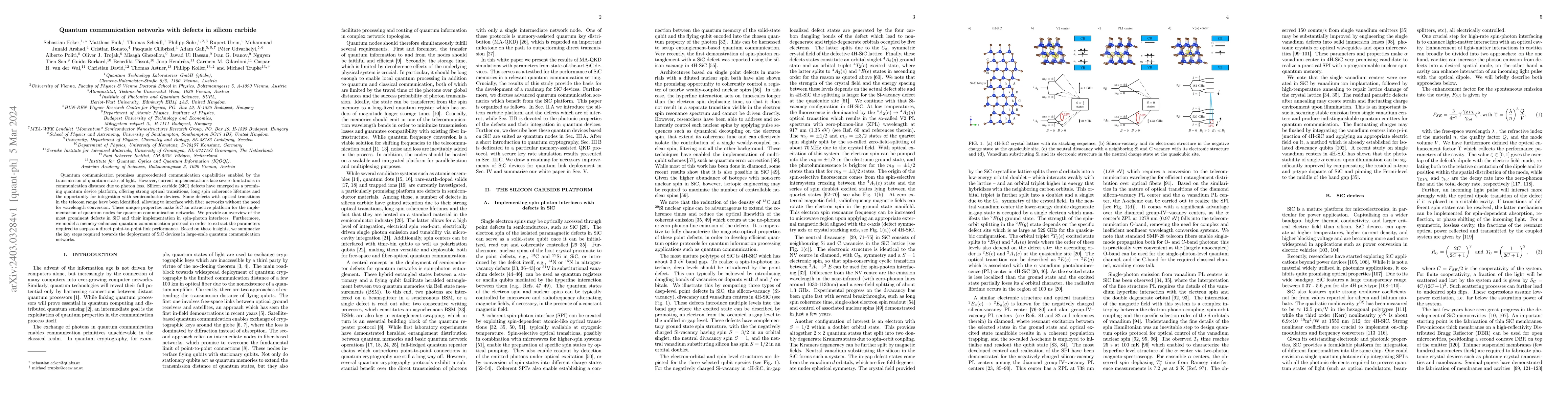
Quantum communication promises unprecedented communication capabilities enabled by the transmission of quantum states of light. However, current implementations face severe limitations in communicat...
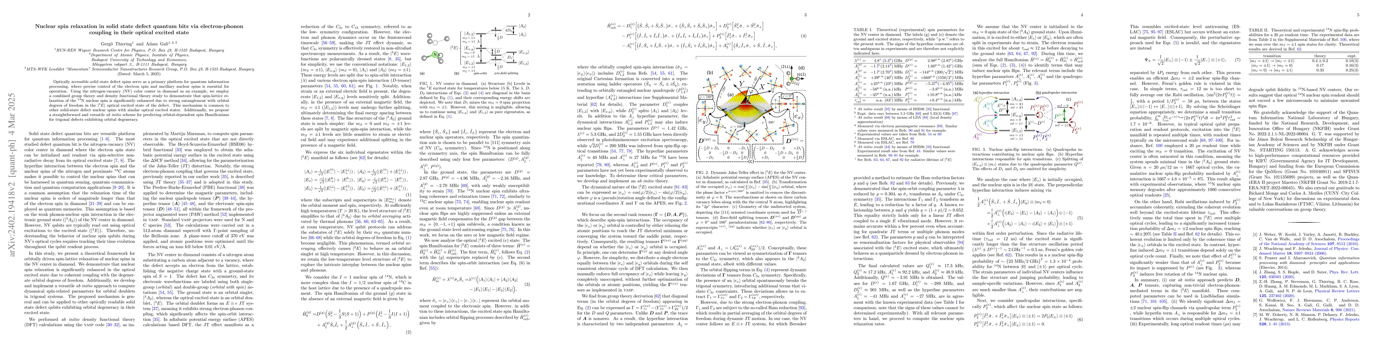
Optically accessible solid state defect spins are primary platform for quantum information processing where tight control of the electron spin and ancilla nuclear spins is pivotal for the operation....
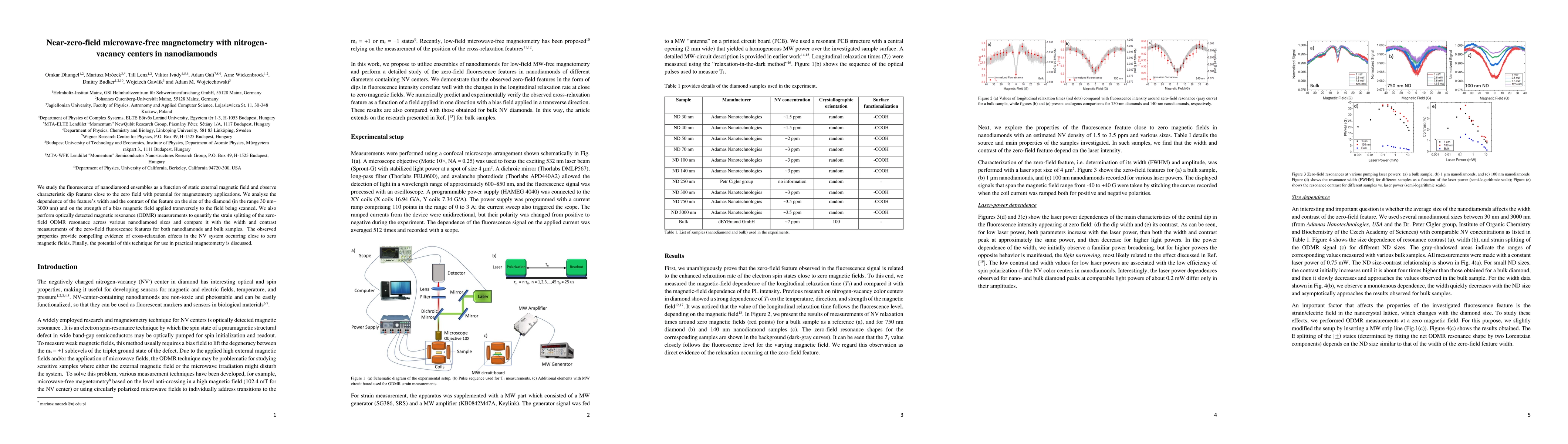
We study the fluorescence of nanodiamond ensembles as a function of static external magnetic field and observe characteristic dip features close to the zero field with potential for magnetometry app...
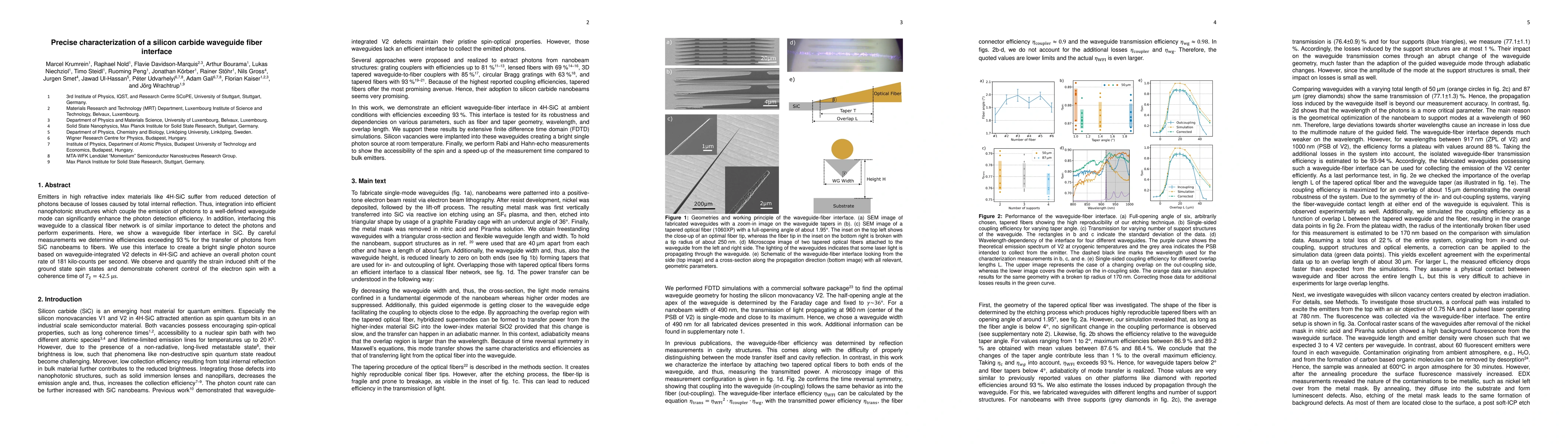
Emitters in high refractive index materials like 4H-SiC suffer from reduced detection of photons because of losses caused by total internal reflection. Thus, integration into efficient nanophotonic ...
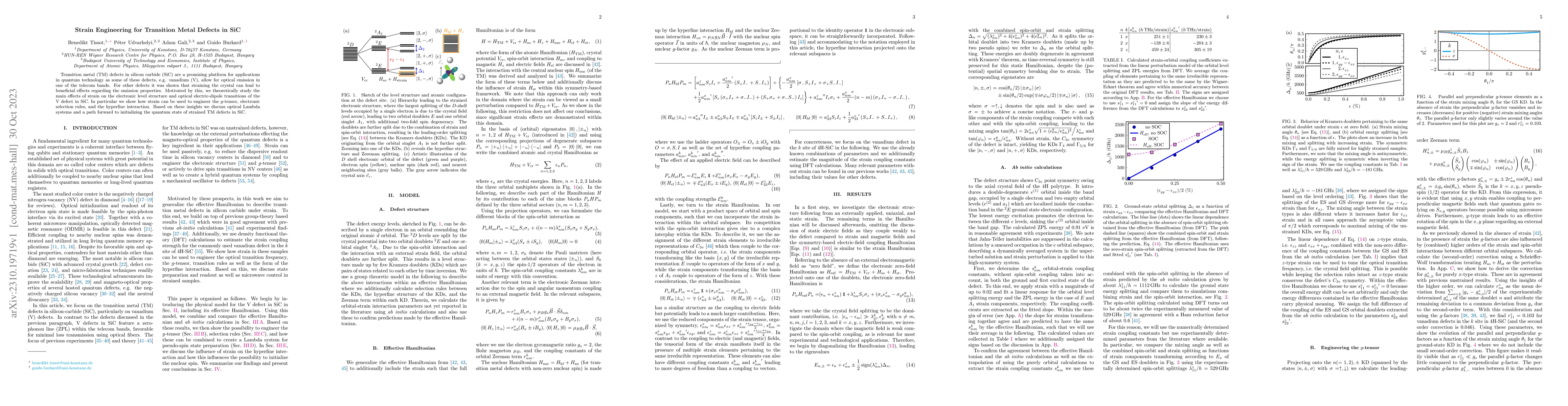
Transition metal (TM) defects in silicon carbide (SiC) are a promising platform for applications in quantum technology as some of these defects, e.g. vanadium (V), allow for optical emission in one ...
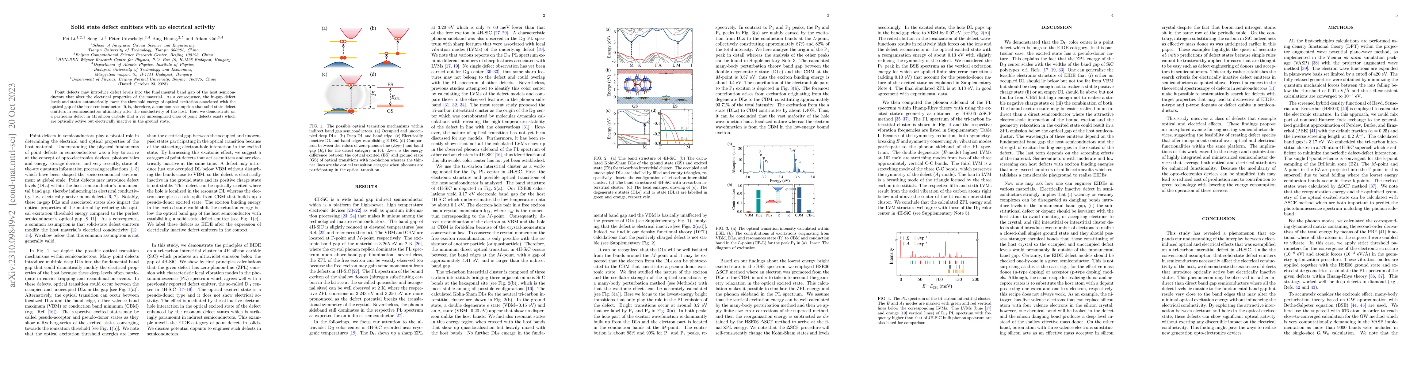
Point defects may introduce defect levels into the fundamental band gap of the host semiconductors that alter the electrical properties of the material. As a consequence, the in-gap defect levels an...
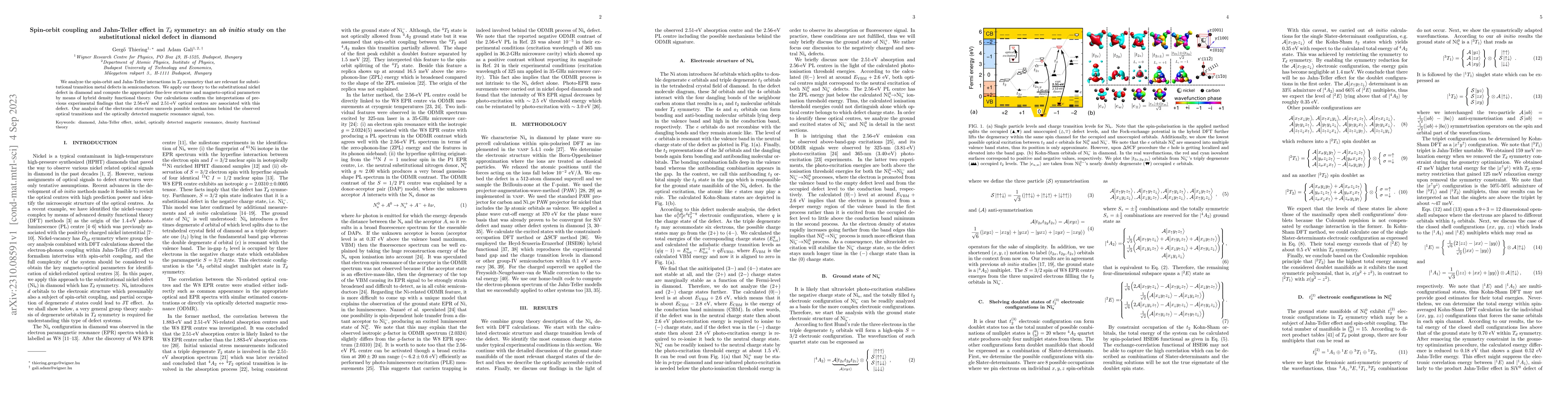
We analyze the spin-orbit and Jahn-Teller interactions in $T_d$ symmetry that are relevant for substitutional transition metal defects in semiconductors. We apply our theory to the substitutional ni...
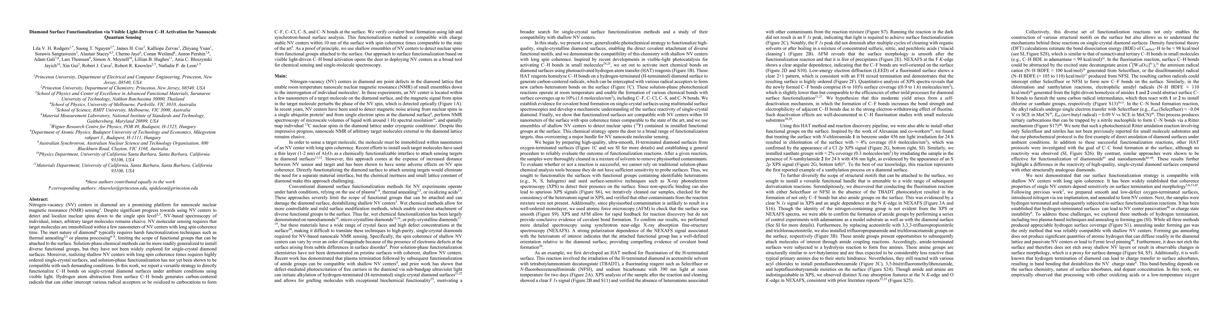
Nitrogen-vacancy centers in diamond are a promising platform for nanoscale nuclear magnetic resonance sensing. Despite significant progress towards using NV centers to detect and localize nuclear sp...
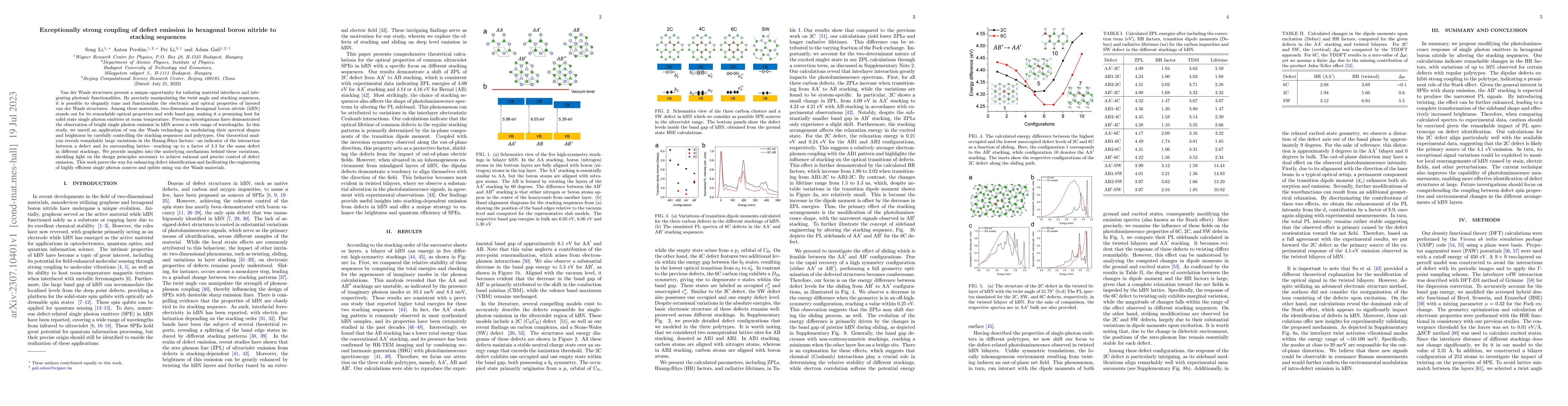
Van der Waals structures present a unique opportunity for tailoring material interfaces and integrating photonic functionalities. By precisely manipulating the twist angle and stacking sequences, it...
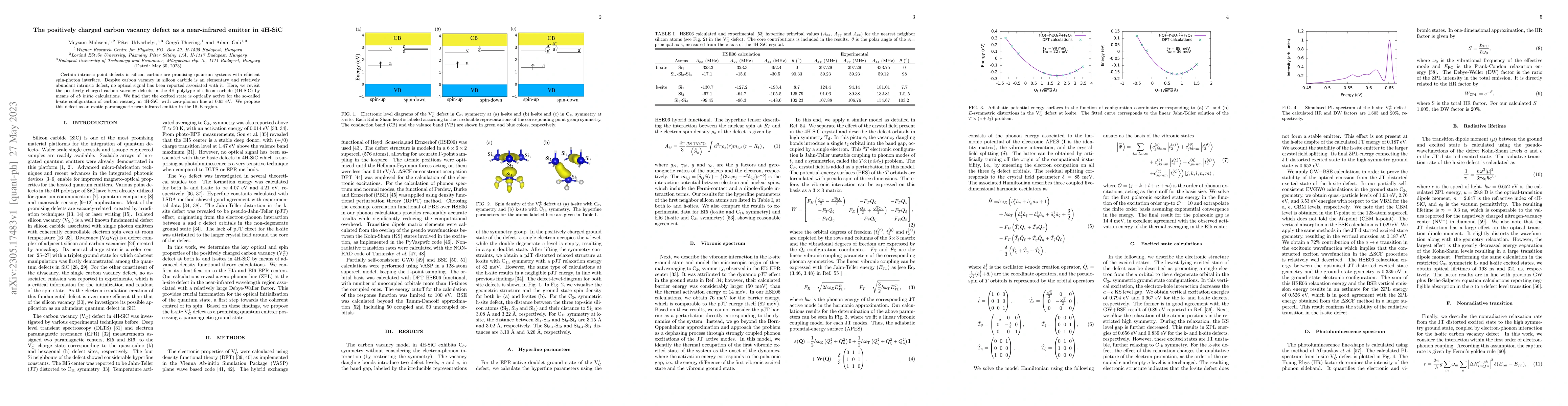
Certain intrinsic point defects in silicon carbide are promising quantum systems with efficient spin-photon interface. Despite carbon vacancy in silicon carbide is an elementary and relatively abund...
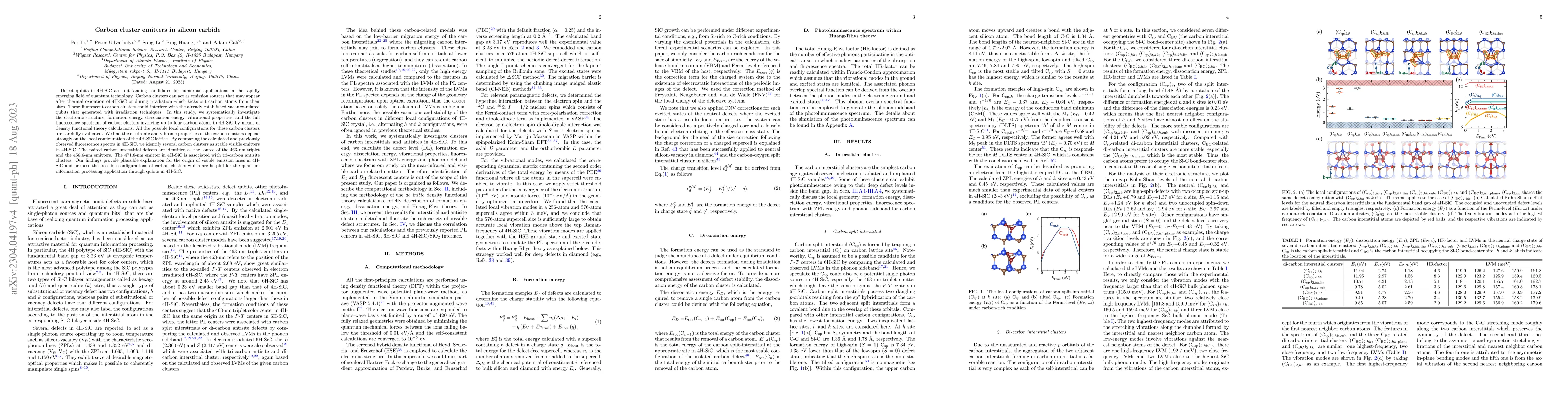
Defect qubits in 4H-SiC are outstanding candidates for numerous applications in the rapidly emerging field of quantum technology. Carbon clusters can act as emission sources that may appear after th...
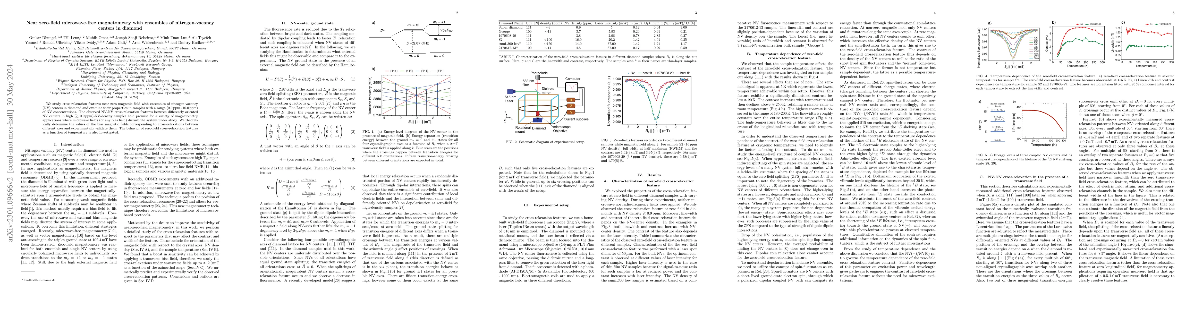
We study cross-relaxation features near zero magnetic field with ensembles of nitrogen-vacancy (NV) centers in diamond and examine their properties in samples with a range (0.9 ppm - 16.0 ppm) of NV...
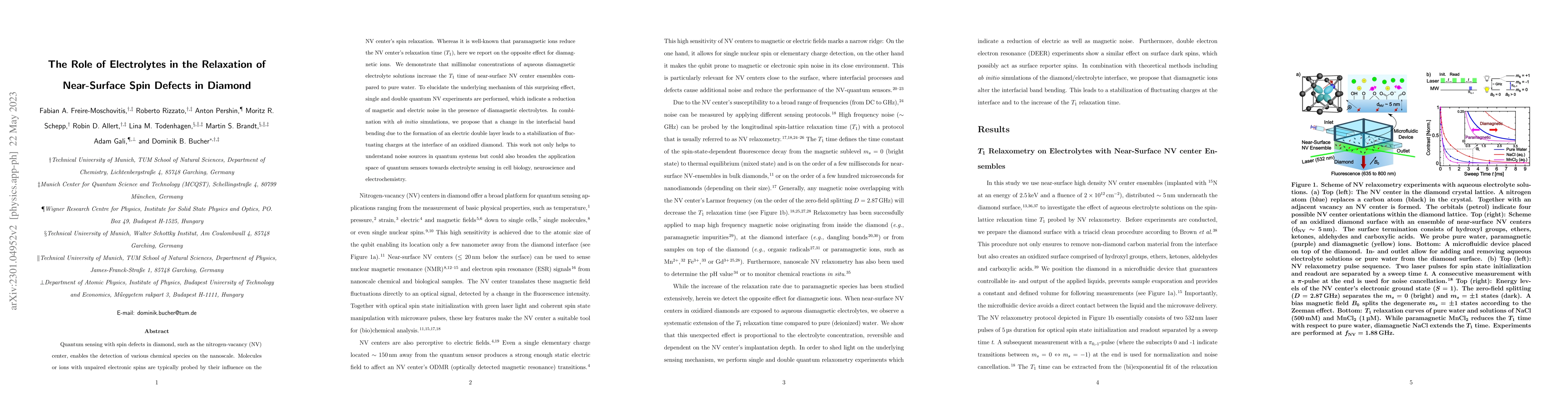
Quantum sensing with spin defects in diamond, such as the nitrogen-vacancy (NV) center, enables the detection of various chemical species on the nanoscale. Molecules or ions with unpaired electronic...
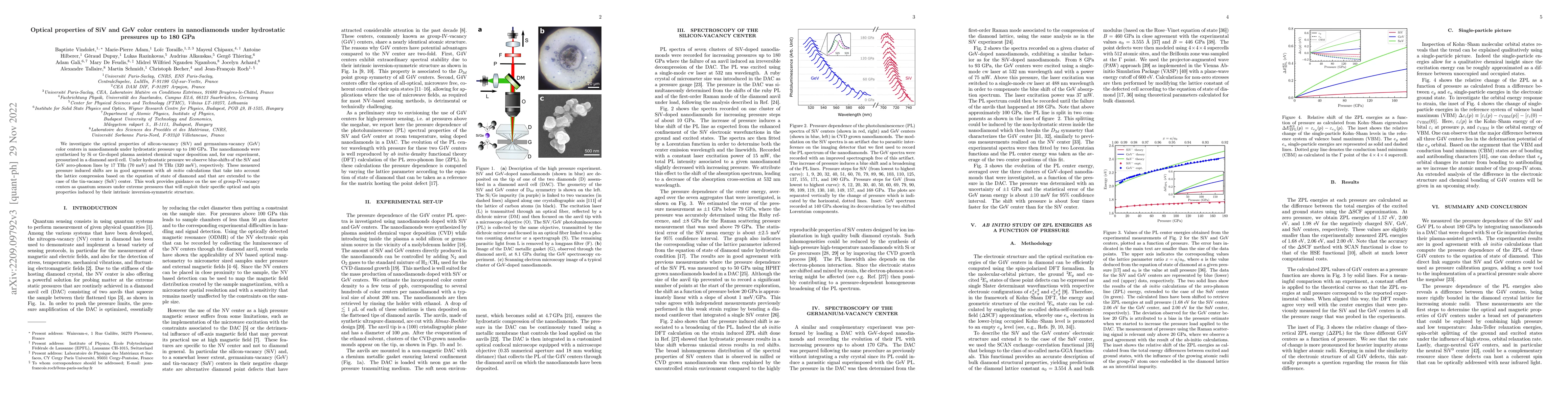
We investigate the optical properties of silicon-vacancy (SiV) and germanium-vacancy (GeV) color centers in nanodiamonds under hydrostatic pressure up to 180 GPa. The nanodiamonds were synthetized b...
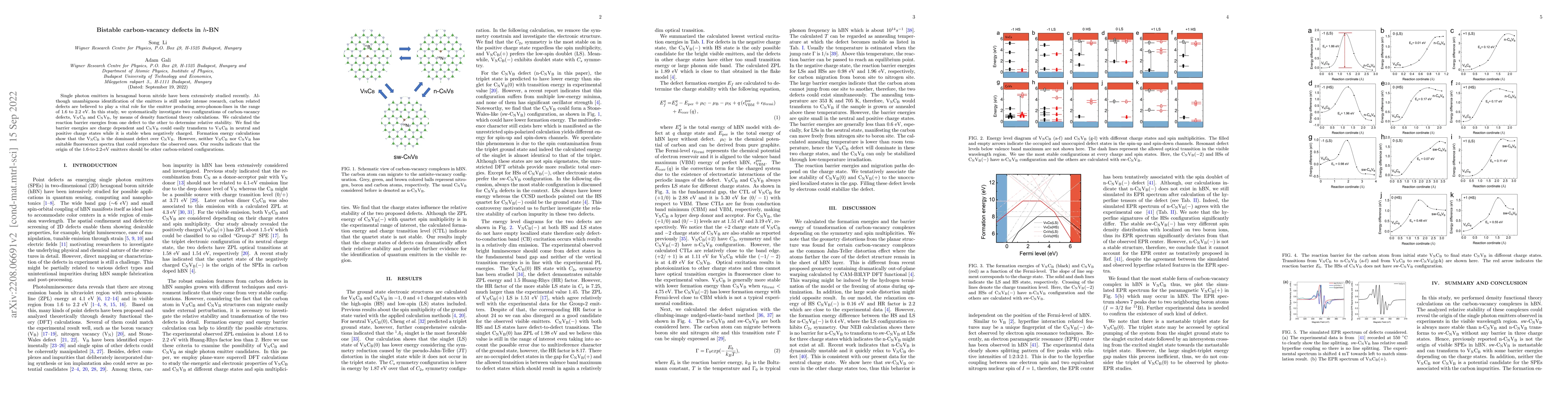
Single photon emitters in hexagonal boron nitride have been extensively studied recently. Although unambiguous identification of the emitters is still under intense research, carbon related defects ...
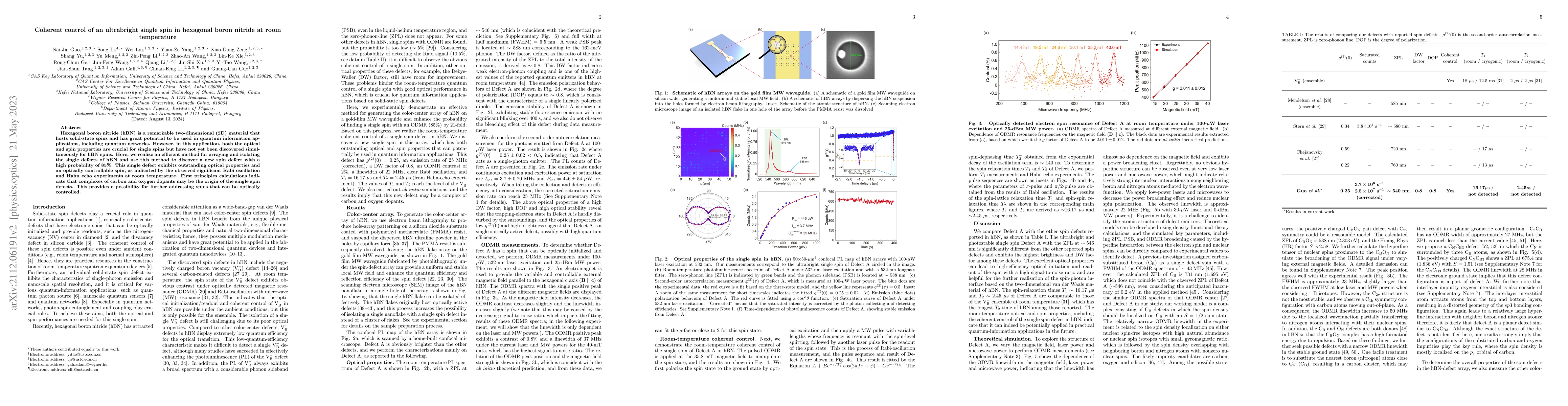
Hexagonal boron nitride (hBN) is a remarkable two-dimensional (2D) material that hosts solid-state spins and has great potential to be used in quantum information applications, including quantum net...
Point defect qubits in semiconductors have demonstrated their outstanding high spatial resolution sensing capabilities of broad multidisciplinary interest. Two-dimensional (2D) semiconductors hostin...
Ultraviolet (UV) quantum emitters in hexagonal boron nitride (hBN) have generated considerable interest due to their outstanding optical response. Recent experiments have identified a carbon impurit...
Unpaired electronic spins at diamond surfaces are ubiquitous and can lead to excess magnetic noise. They have been observed in several studies to date, but their exact chemical nature is still unkno...
Controlling the quantum properties of individual fluorescent defects in silicon is a key challenge towards advanced quantum photonic devices prone to scalability. Research efforts have so far focuse...
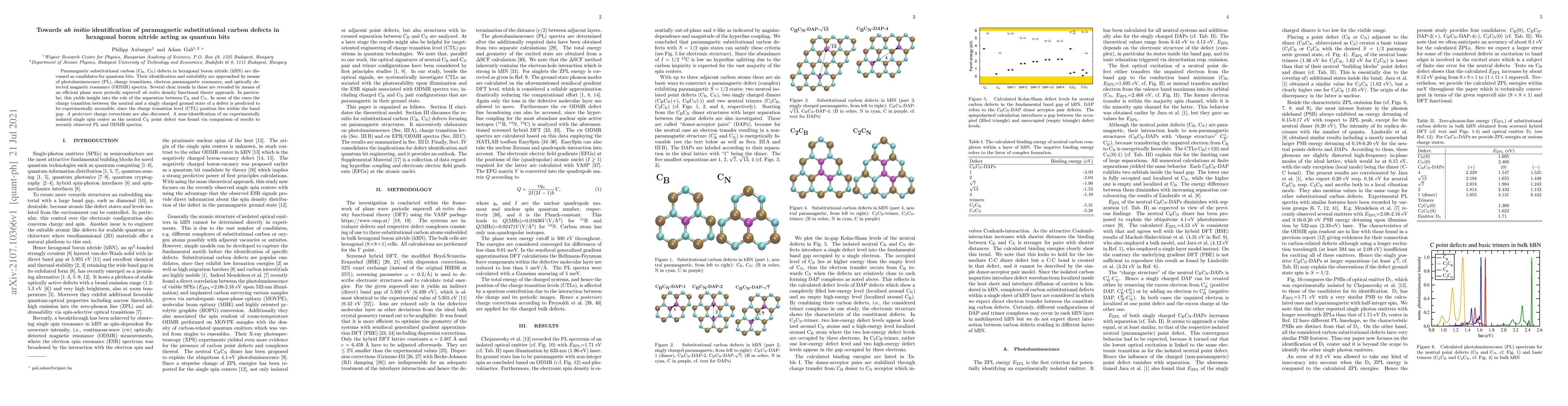
Paramagnetic substitutional carbon (C$_\text{B}$, C$_\text{N}$) defects in hexagonal boron nitride (hBN) are discussed as candidates for quantum bits. Their identification and suitability are approa...
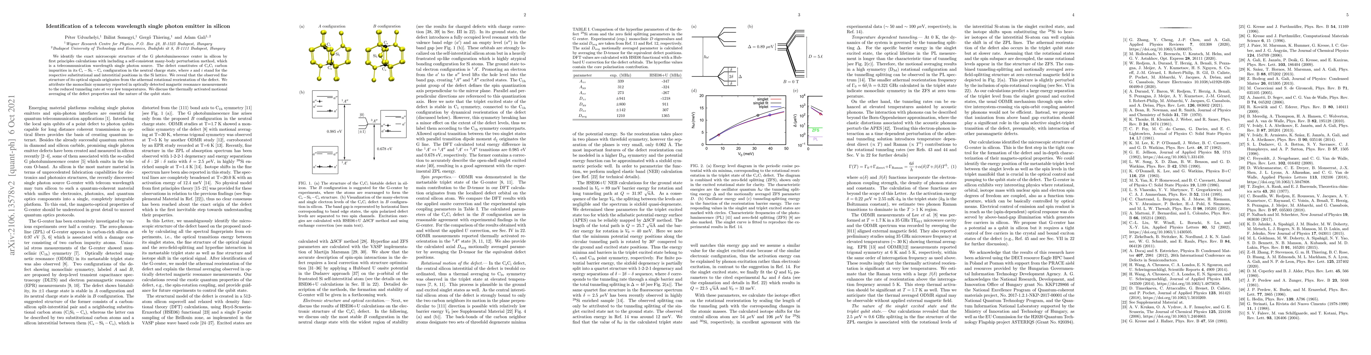
We identify the exact microscopic structure of the G photoluminescence center in silicon by first principles calculations with including a self-consistent many-body perturbation method, which is a t...
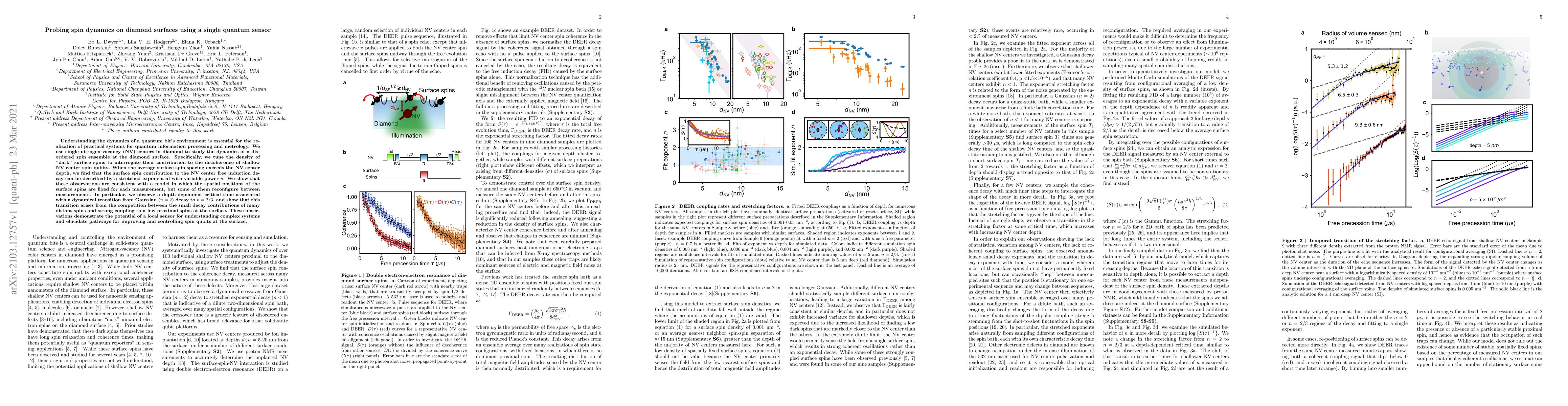
Understanding the dynamics of a quantum bit's environment is essential for the realization of practical systems for quantum information processing and metrology. We use single nitrogen-vacancy (NV) ...
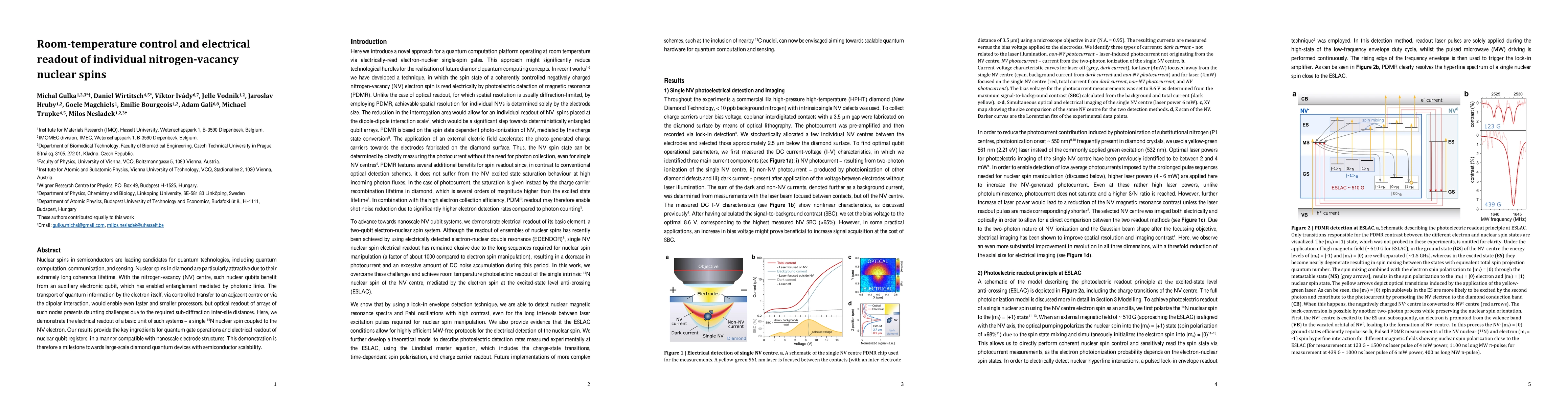
Nuclear spins in semiconductors are leading candidates for quantum technologies, including quantum computation, communication, and sensing. Nuclear spins in diamond are particularly attractive due t...
Defects with associated electron and nuclear spins in solid-state materials have a long history relevant to quantum information science going back to the first spin echo experiments with silicon dop...
Many quantum emitters have been measured close or near the grain boundaries of the two-dimensional hexagonal boron nitride where various Stone-Wales defects appear. We show by means of first princip...
Quantum technology has grown out of quantum information theory and now provides a valuable tool that researchers from numerous fields can add to their toolbox of research methods. To date, various s...
Recently, vacancy-related spin defects in silicon carbide (SiC) have been demonstrated to be potentially suitable for versatile quantum interface building and scalable quantum network construction. ...
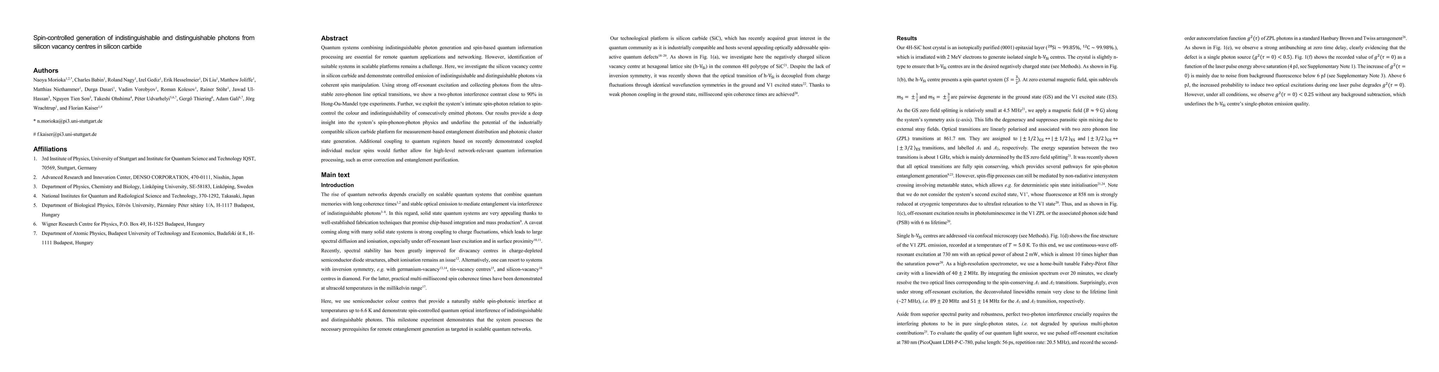
Quantum systems combining indistinguishable photon generation and spin-based quantum information processing are essential for remote quantum applications and networking. However, identification of s...
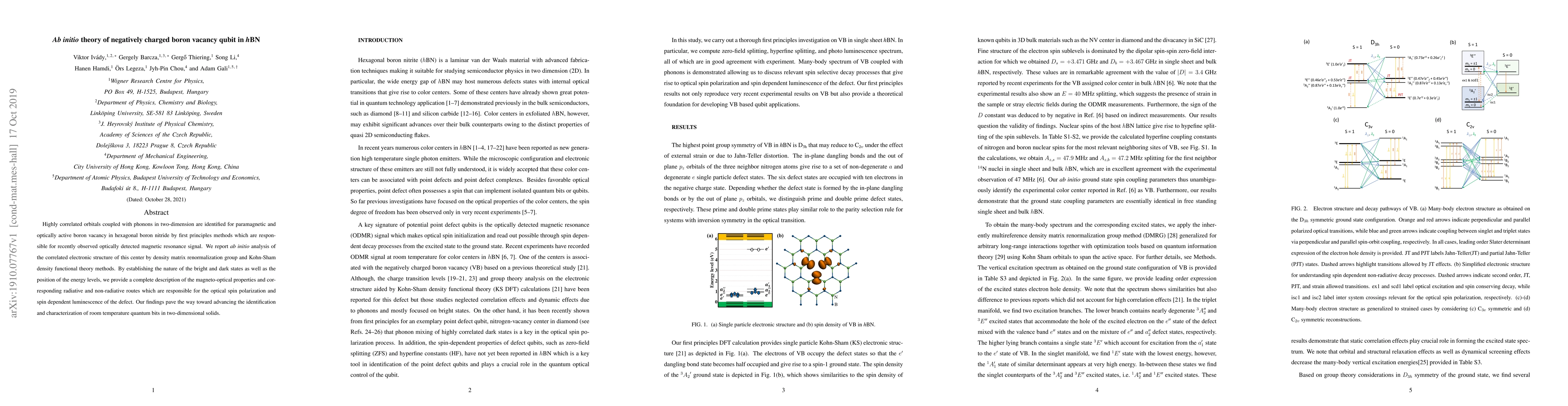
Highly correlated orbitals coupled with phonons in two-dimension are identified for paramagnetic and optically active boron vacancy in hexagonal boron nitride by first principles methods which are r...
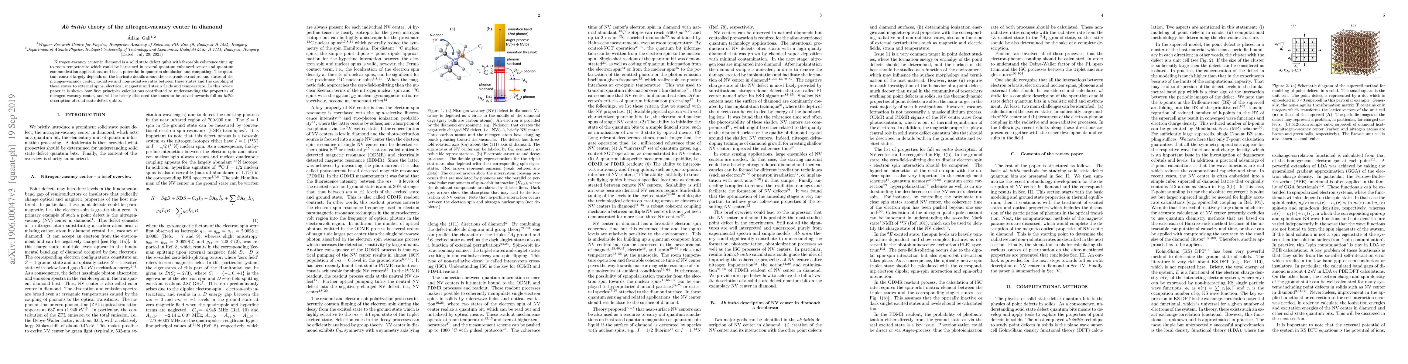
Nitrogen-vacancy center in diamond is a solid state defect qubit with favorable coherence time up to room temperature which could be harnessed in several quantum enhanced sensor and quantum communic...
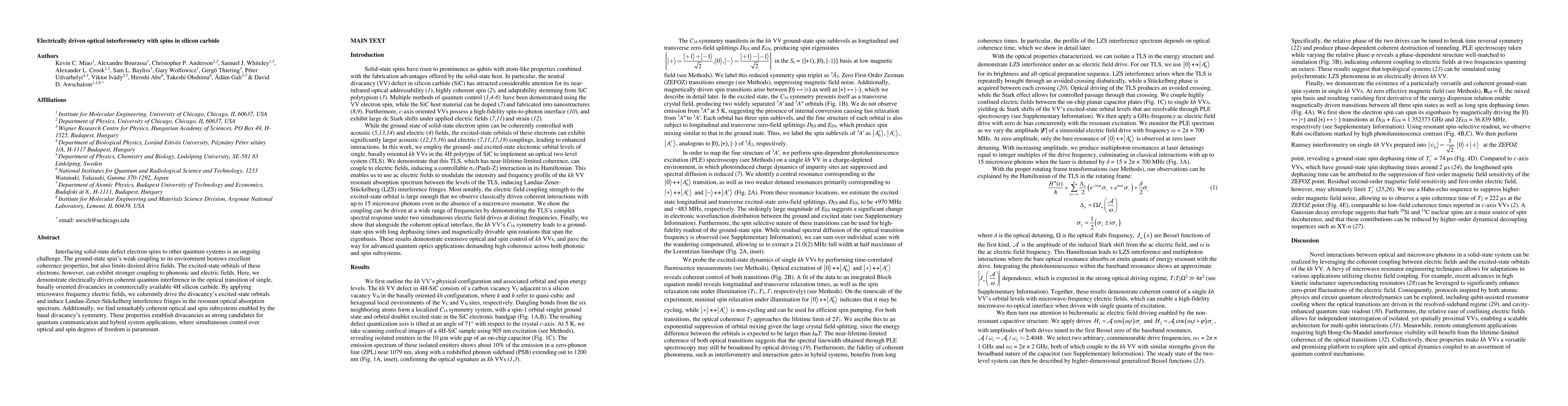
Interfacing solid-state defect electron spins to other quantum systems is an ongoing challenge. The ground-state spin's weak coupling to its environment bestows excellent coherence properties, but a...
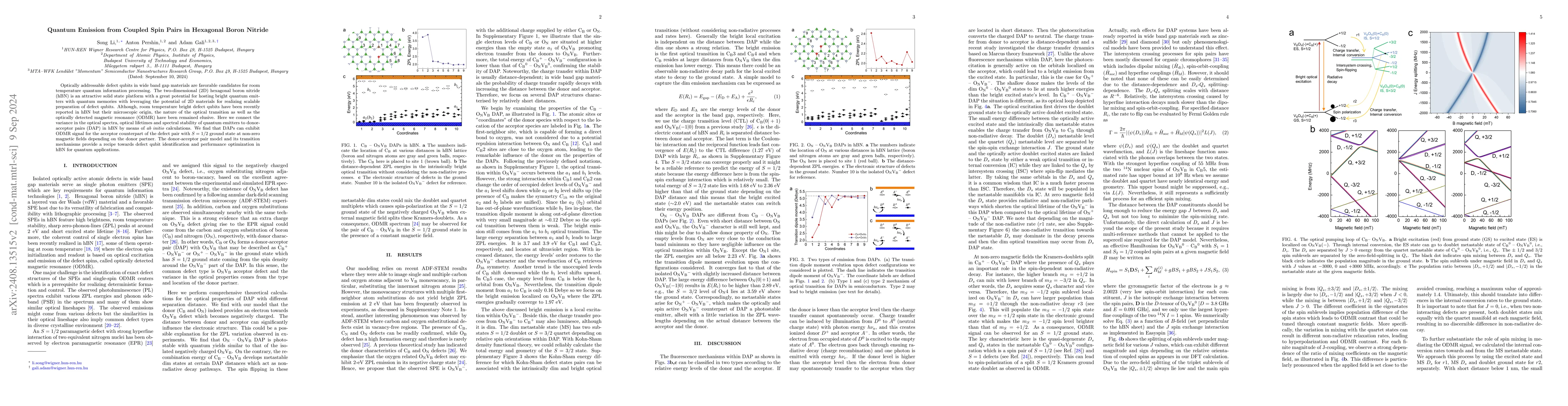
Optically addressable defect qubits in wide band gap materials are favorable candidates for room temperature quantum information processing. The two-dimensional (2D) hexagonal boron nitride (hBN) is a...
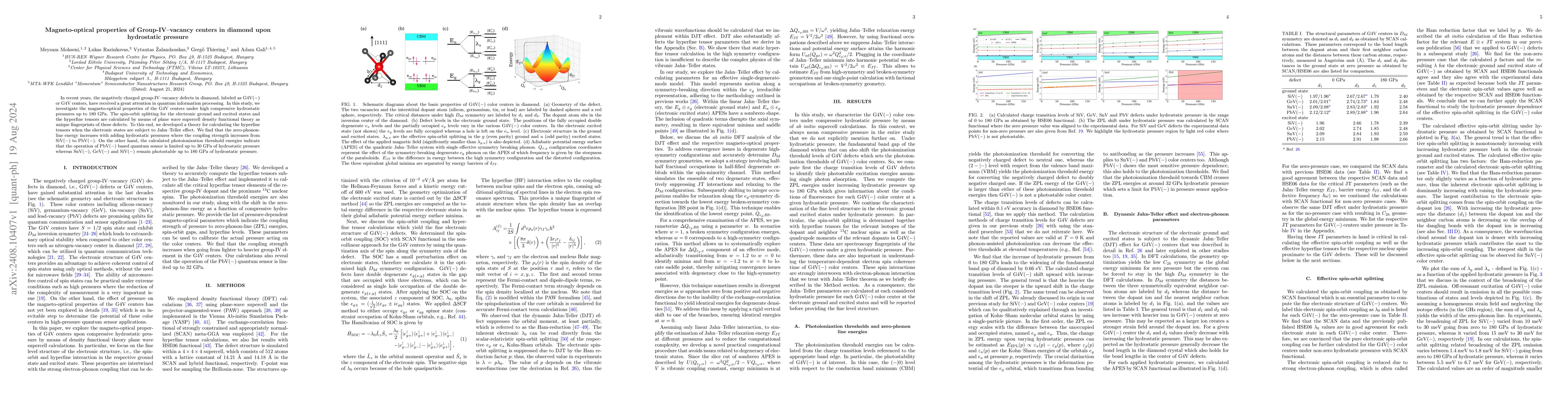
In recent years, the negatively charged group-IV--vacancy defects in diamond, labeled as G4V($-$) or G4V centers, have received a great attention in quantum information processing. In this study, we i...
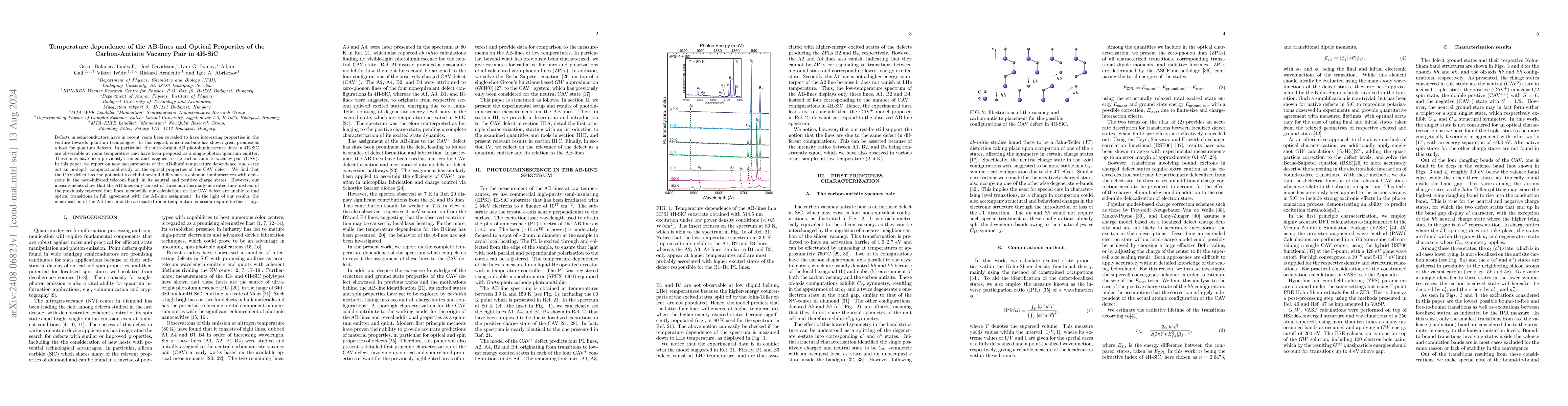
Defects in semiconductors have in recent years been revealed to have interesting properties in the venture towards quantum technologies. In this regard, silicon carbide has shown great promise as a ho...
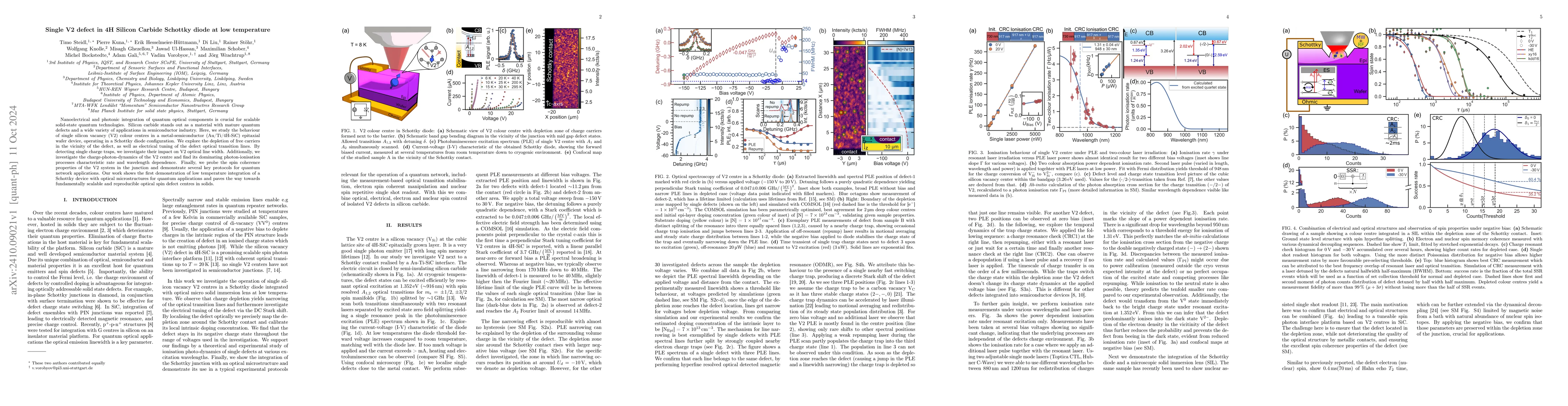
Nanoelectrical and photonic integration of quantum optical components is crucial for scalable solid-state quantum technologies. Silicon carbide stands out as a material with mature quantum defects and...
Hexagonal boron nitride (hBN) is an excellent host for solid-state single phonon emitters. Experimental observed emission ranges from infrared to ultraviolet. The emission centers are generally attrib...
Recent advances in the engineering of diamond surface make it possible to stabilize the charge state of 7-30 nanometers deep nitrogen-vacancy (NV) quantum sensors in diamond and to principally remove ...
Understanding and controlling fluorescent nanodiamonds (FNDs) with optically read qubits is a key focus of research, as they show high potential for detecting electric and magnetic fields, temperature...
In this study, we implement thiol termination on the surface of few-nanometer-sized silicon carbide (SiC) nanoparticles (NPs) to enable further applications, such as fluorescent biomarkers. Various sp...
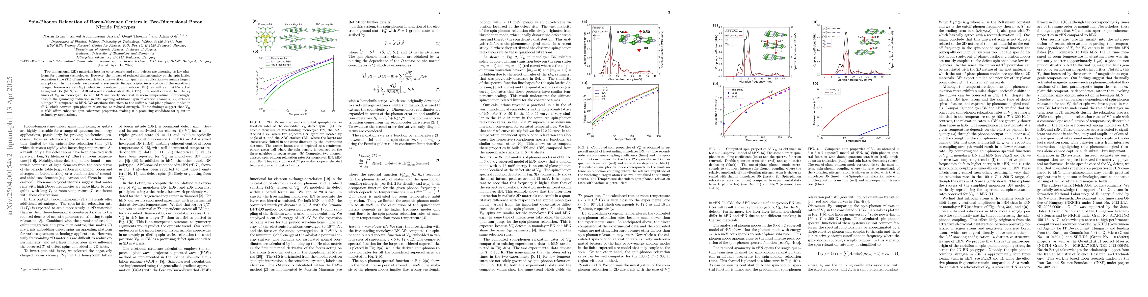
Two-dimensional (2D) materials hosting color centers and spin defects are emerging as key platforms for quantum technologies. However, the impact of reduced dimensionality on the spin-lattice relaxati...
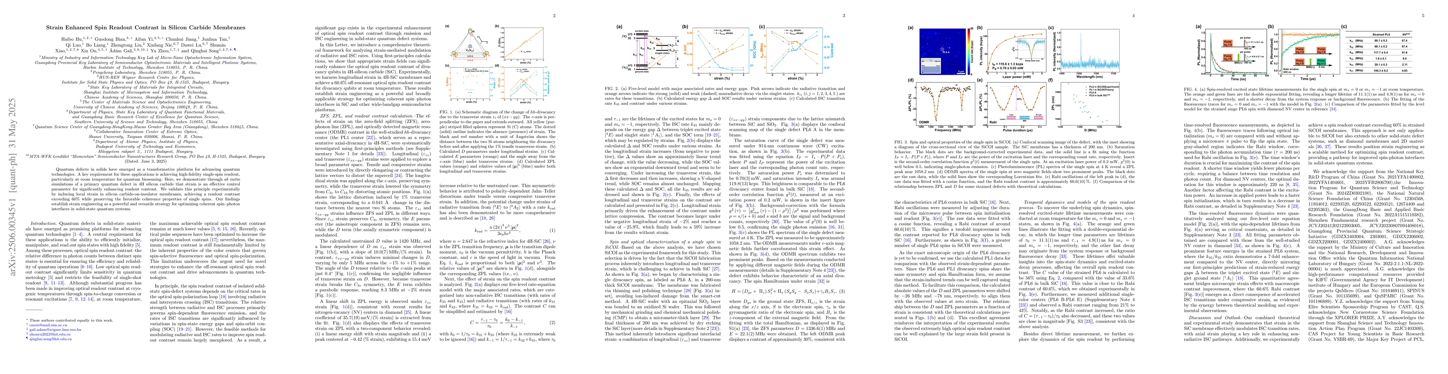
Quantum defects in solids have emerged as a transformative platform for advancing quantum technologies. A key requirement for these applications is achieving high-fidelity single-spin readout, particu...
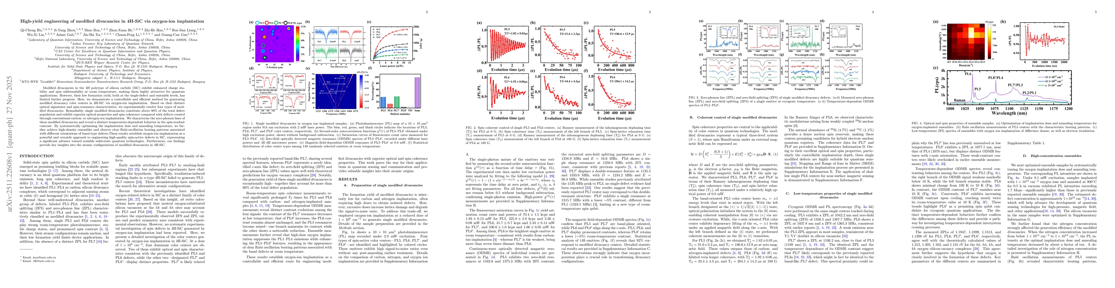
Modified divacancies in the 4H polytype of silicon carbide (SiC) exhibit enhanced charge stability and spin addressability at room temperature, making them highly attractive for quantum applications. ...
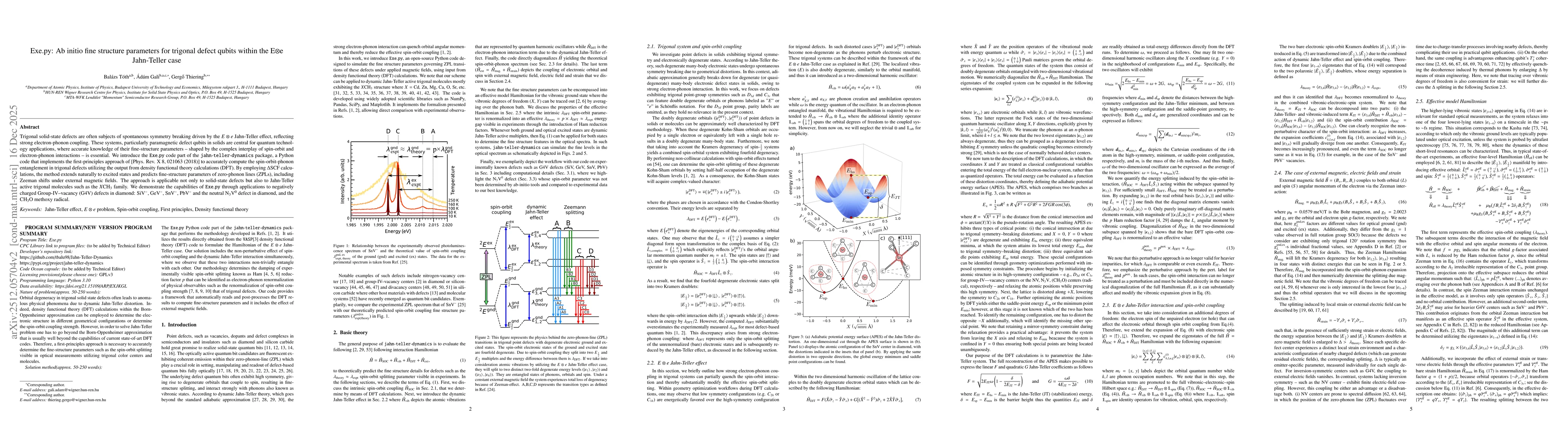
Trigonal solid-state defects are often subjects of spontaneous symmetry breaking driven by the $E\otimes e$ Jahn-Teller effect, reflecting strong electron-phonon coupling. These systems, particularly ...
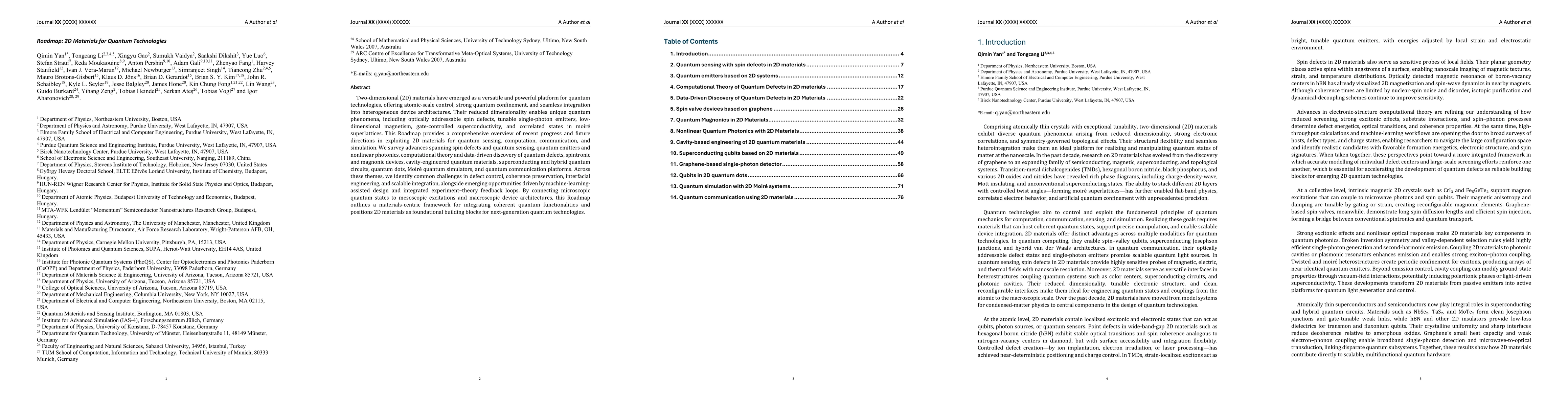
Two-dimensional (2D) materials have emerged as a versatile and powerful platform for quantum technologies, offering atomic-scale control, strong quantum confinement, and seamless integration into hete...
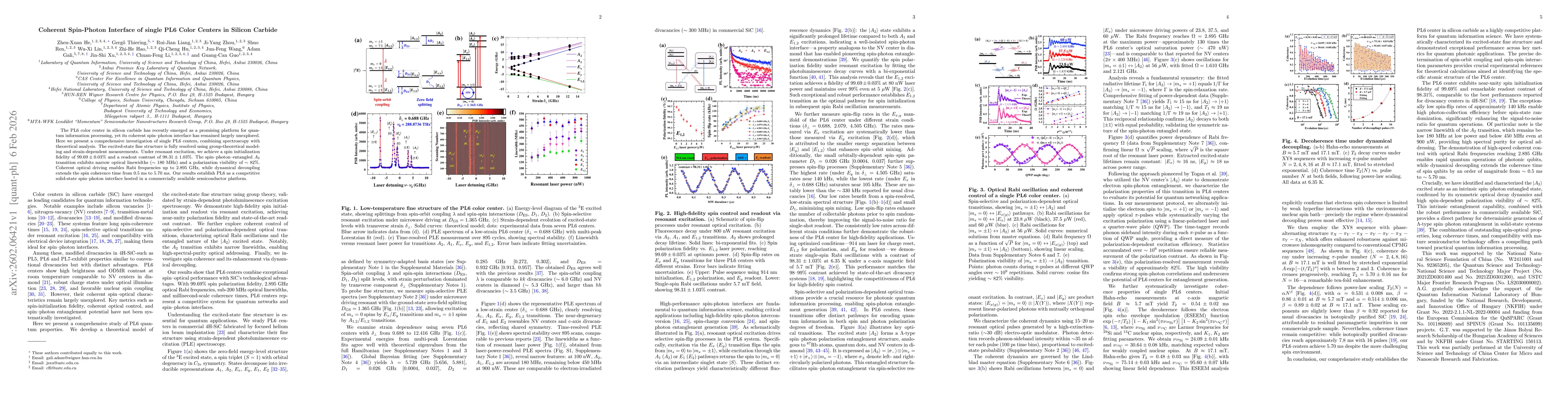
The PL6 color center in silicon carbide has recently emerged as a promising platform for quantum information processing, yet its coherent spin--photon interface has remained largely unexplored. Here w...
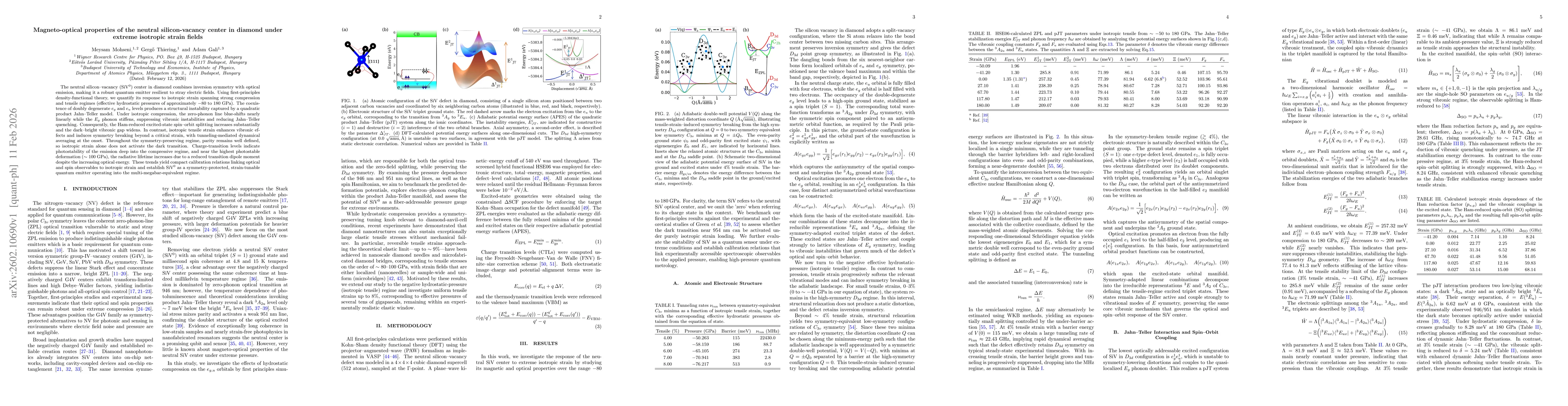
The neutral silicon--vacancy (SiV$^{0}$) center in diamond combines inversion symmetry with optical emission, making it a robust quantum emitter resilient to stray electric fields. Using first-princip...
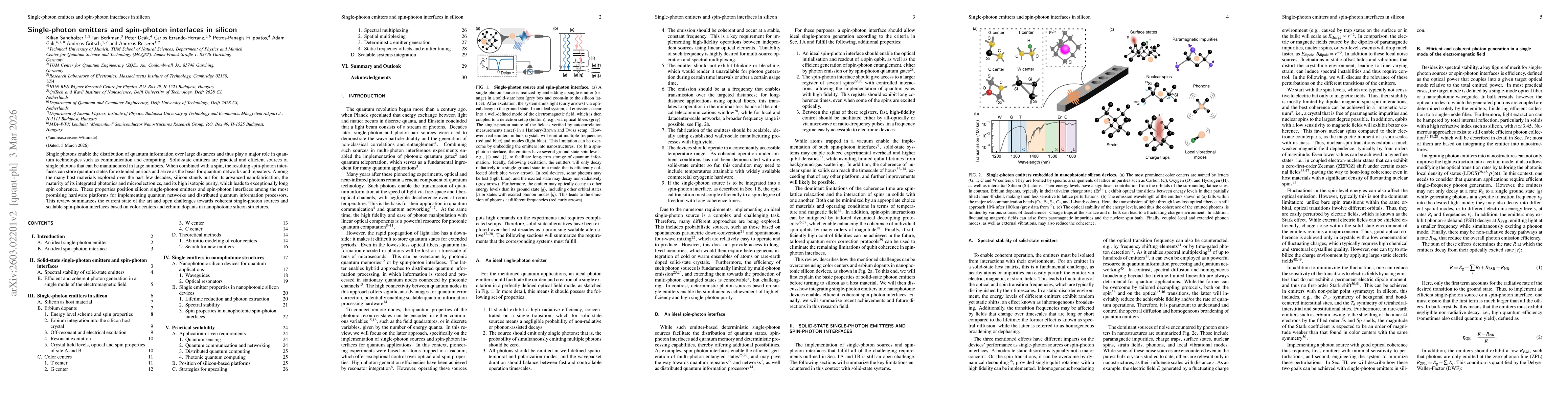
Single photons enable the distribution of quantum information over large distances and thus play a major role in quantum technologies such as communication and computing. Solid-state emitters are prac...
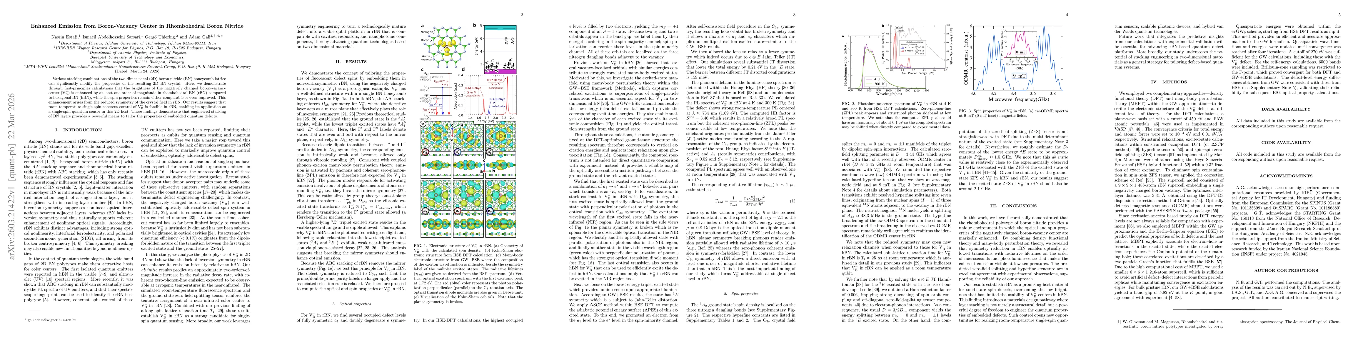
Various stacking combinations of the two-dimensional (2D) boron nitride (BN) honeycomb lattice can significantly modify the properties of the resulting 2D BN crystal. Here, we demonstrate through firs...
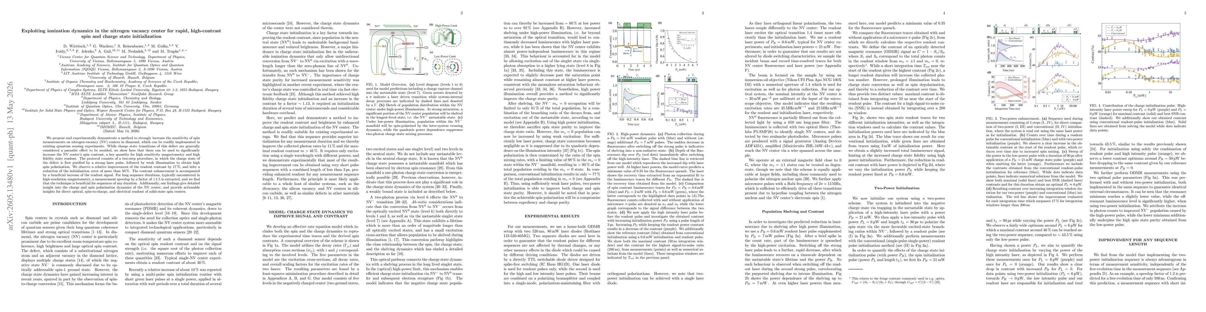
We propose and experimentally demonstrate a method to strongly increase the sensitivity of spin measurements on nitrogen-vacancy (NV) centers in diamond, which can be readily implemented in existing q...
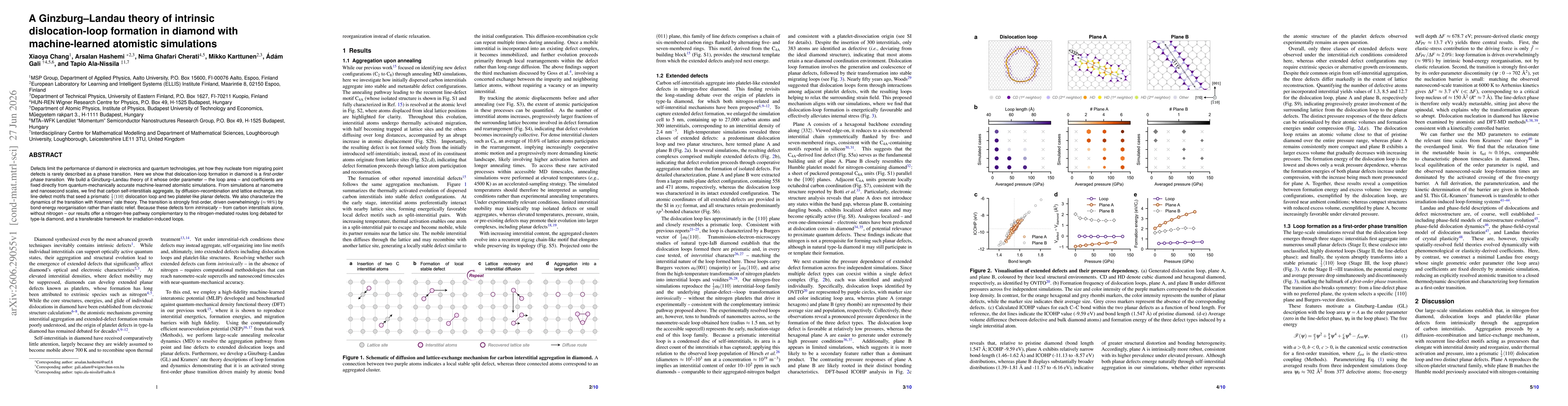
Defects limit the performance of diamond in electronics and quantum technologies, yet how they nucleate from migrating point defects is rarely described as a phase transition. Here we show that disloc...