Academic Profile
Statistics
Similar Authors
Papers on arXiv
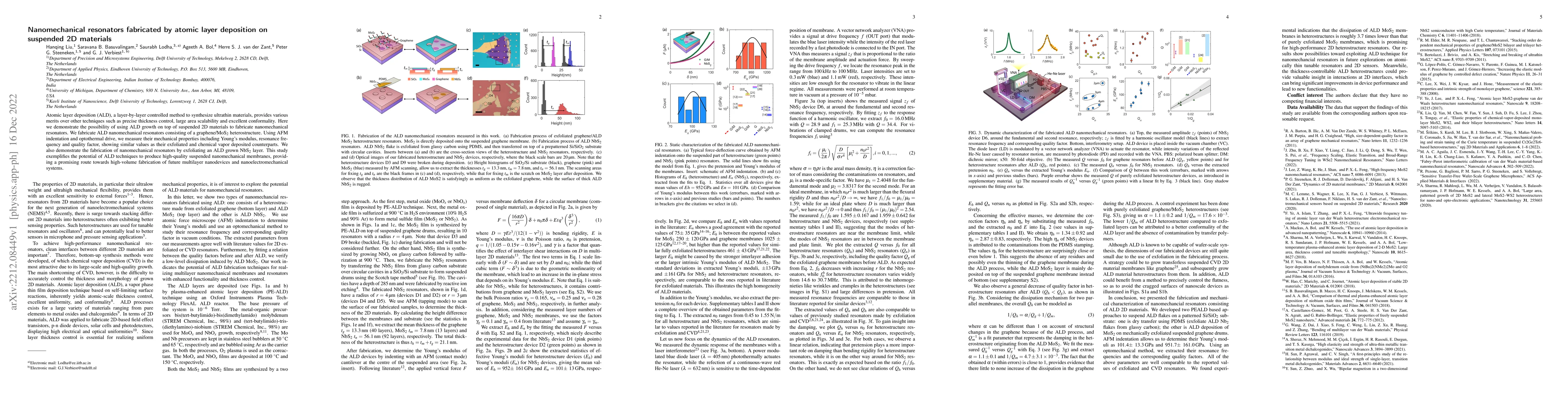
Atomic layer deposition (ALD), a layer-by-layer controlled method to synthesize ultrathin materials, provides various merits over other techniques such as precise thickness control, large area scala...
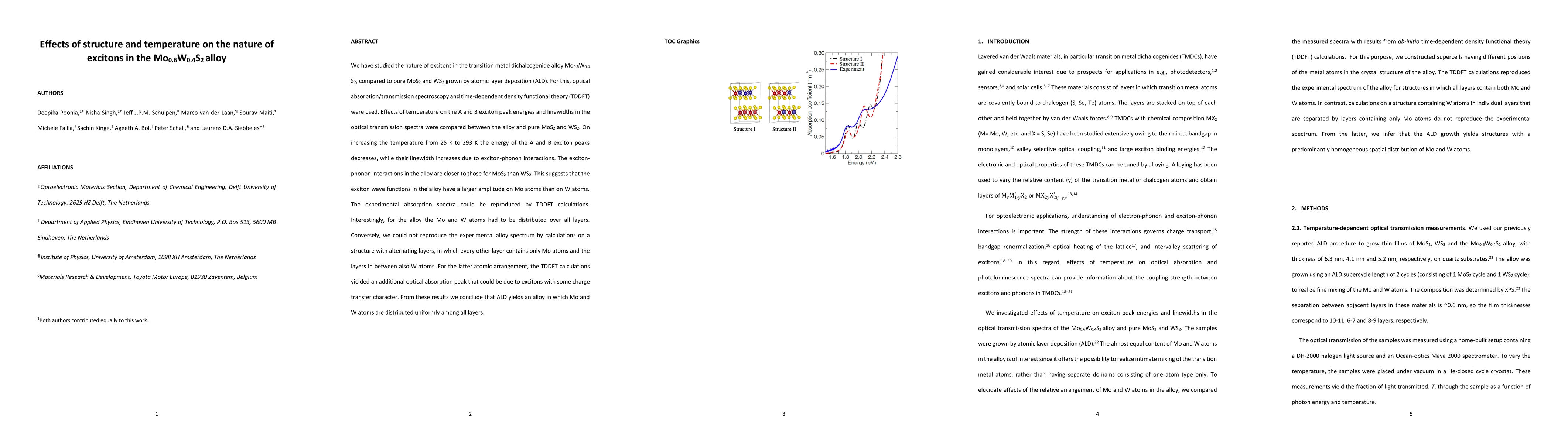
We have studied the nature of excitons in the transition metal dichalcogenide alloy Mo0.6W0.4 S2, compared to pure MoS2 and WS2 grown by atomic layer deposition (ALD). For this, optical absorption/t...
The unique optical and electronic properties of two-dimensional transition metal dichalcogenides (2D TMDs) make them promising materials for applications in (opto-)electronics, catalysis and more. S...
We demonstrate the extensive study on how film density and crystallinity of molybdenum carbide ($MoC_{x}$) can be tailored during plasma-enhanced ALD (PEALD) by controlling either the plasma exposur...
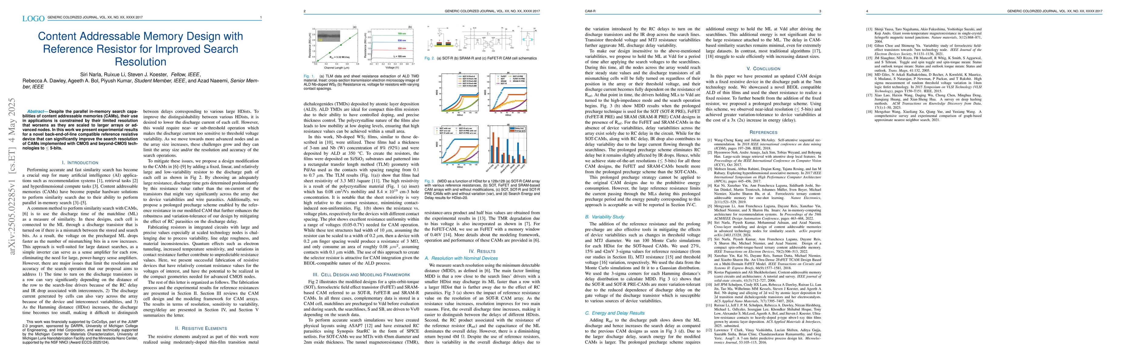
Despite the parallel in-memory search capabilities of content addressable memories (CAMs), their use in applications is constrained by their limited resolution that worsens as they are scaled to large...
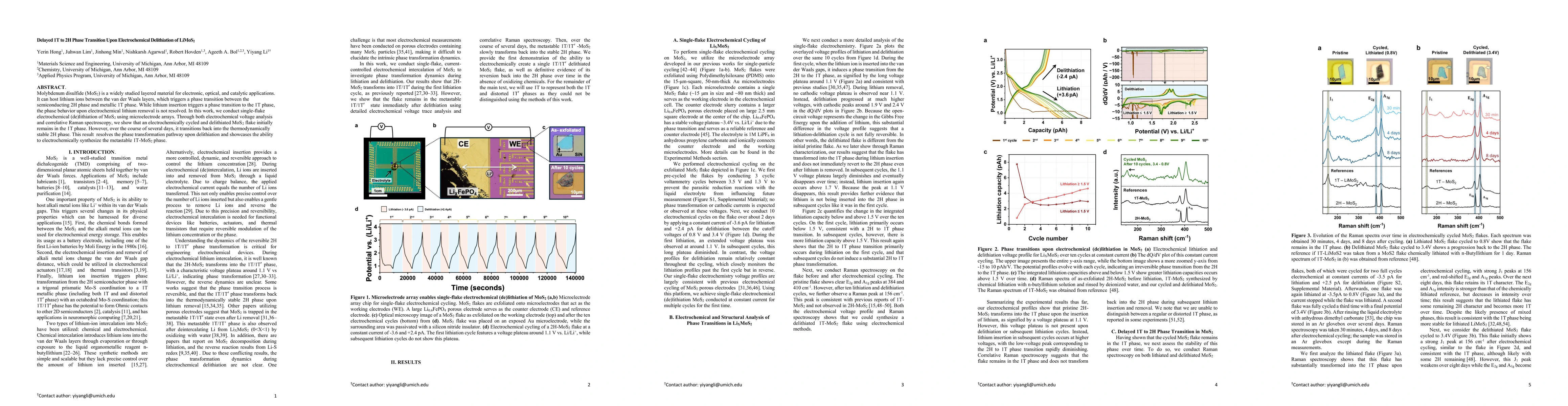
Molybdenum disulfide (MoS2) is a widely studied layered material for electronic, optical, and catalytic applications. It can host lithium ions between the van der Waals layers, which triggers a phase ...
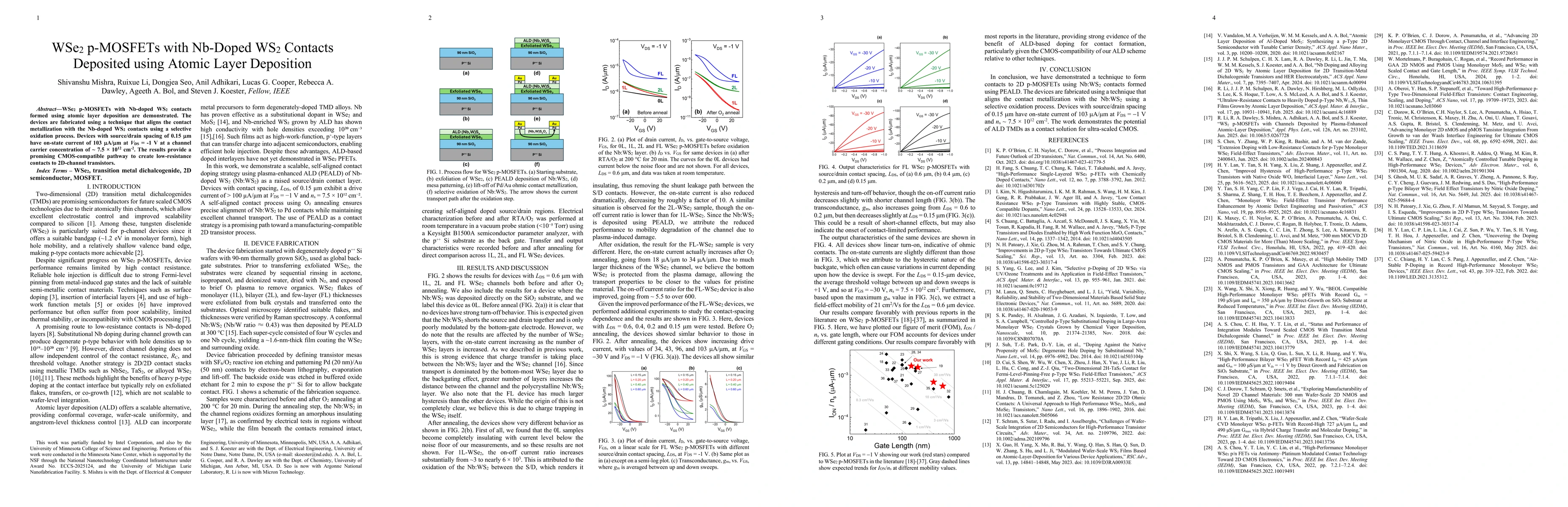
WSe2 p-MOSFETs with Nb-doped WS2 contacts formed using atomic layer deposition are demonstrated. The devices are fabricated using a technique that aligns the contact metallization with the Nb-doped WS...