Academic Profile
Statistics
Similar Authors
Papers on arXiv
We systematically investigated the growth of Si-doped $\beta$-Ga$_2$O$_3$ films using LPCVD system, achieving high electron mobilities of 162 cm$^2$/V.s and 149 cm$^2$/V.s at carrier concentrations of...
In the rapidly evolving field of quantum computing, niobium nitride (NbN) superconductors have emerged as integral components due to their unique structural properties, including a high superconductin...
This work demonstrates a novel in situ etching technique for $\beta$-Ga$_2$O$_3$ using solid-source metallic Ga in a LPCVD system, enabling clean, anisotropic, plasma damage-free etching. Etching beha...
This work demonstrates quasi-vertical beta-Ga2O3 Schottky barrier diodes (SBDs) fabricated on c-plane sapphire using an all-LPCVD, plasma-free process integrating epitaxial growth of high-quality beta...
This study investigates the impact of fast neutron irradiation and post-radiation electro-thermal annealing on the electrical performance of $\beta$-Ga$_2$O$_3$ Schottky barrier diodes. Devices irradi...

The integration of diamond with $β$-Ga$_2$O$_3$ presents a promising pathway to enhance thermal management in high-power electronic devices, where the inherently low thermal conductivity of $β$-Ga$_2$...
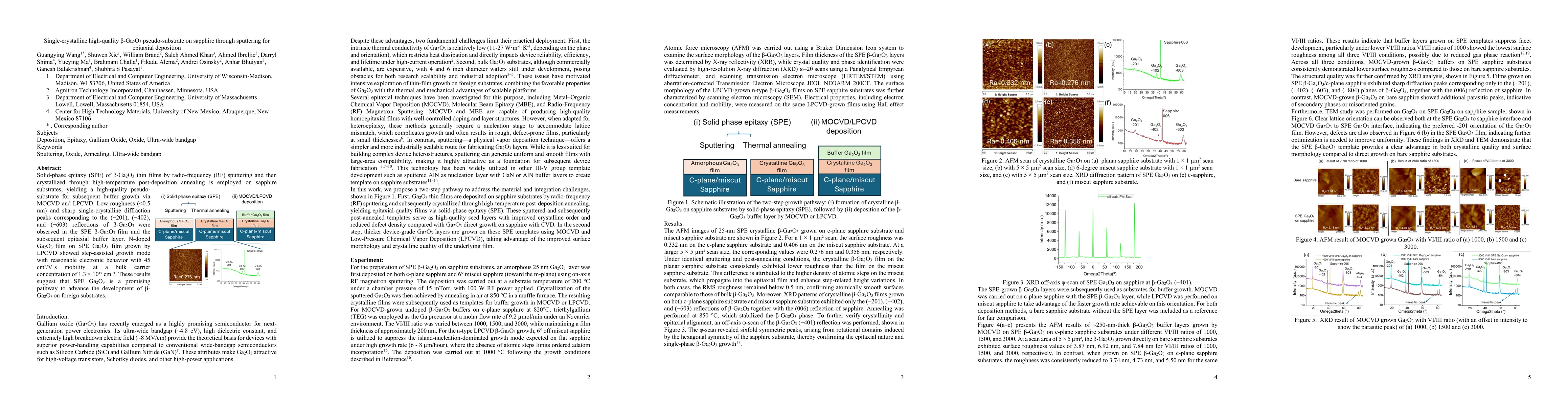
Solid-phase epitaxy (SPE) of beta-Ga2O3 thin films by radio-frequency (RF) sputtering and then crystallized through high-temperature post-deposition annealing is employed on sapphire substrates, yield...
Si-doped $β$-Ga$_2$O$_3$ films were heteroepitaxially grown on sapphire substrates using HVPE. The influence of sapphire offcut on growth kinetics, surface morphology, crystalline quality, and electri...
In this work, we investigate the response of Ni/$β$-Ga$_2$O$_3$ Schottky barrier diodes fabricated on c-plane sapphire to fast-neutron irradiation up to a fluence of $1\times10^{15}$ n$\cdot$cm$^{-2}$...
A deep-etch field termination strategy using a Ga-assisted plasma-free etching technique in a low-pressure chemical vapor deposition (LPCVD) system is demonstrated for $β$-Ga$_2$O$_3$ Schottky barrier...