ArxivLens
A
Researcher

Alex Henning

7 papers on arXiv

7 arXiv Papers
52 Total Publications
Profile

Academic Profile

Name A. Henning
Total Papers 52
Scholar Profile View on Semantic Scholar
Metrics

Statistics

7 arXiv Papers
52 Total Publications
Publications

Papers on arXiv

Thumbnail for Using metal-organic frameworks to confine liquid samples for nanoscale
  NV-NMR
arXiv
Using metal-organic frameworks to confine liquid samples for nanoscale NV-NMR

Atomic-scale magnetic field sensors based on nitrogen vacancy (NV) defects in diamonds are an exciting platform for nanoscale nuclear magnetic resonance (NMR) spectroscopy. The detection of NMR sign...

Thumbnail for Spatially-Modulated Silicon Interface Energetics via Hydrogen
  Plasma-Assisted Atomic Layer Deposition of Ultrathin Alumina
arXiv
Spatially-Modulated Silicon Interface Energetics via Hydrogen Plasma-Assisted Atomic Layer Deposition of Ultrathin Alumina

Atomic layer deposition (ALD) is a key technique for the continued scaling of semiconductor devices, which increasingly relies on reproducible and scalable processes for interface manipulation of 3D...

Thumbnail for Scalable transparent conductive thin films with electronically passive
  interfaces for direct chemical vapor deposition of 2D materials
arXiv
Scalable transparent conductive thin films with electronically passive interfaces for direct chemical vapor deposition of 2D materials

We present a novel transparent conductive support structure for two-dimensional (2D) materials that provides an electronically passive 2D/3D interface while also enabling facile interfacial charge t...

Thumbnail for A Roadmap for Controlled and Efficient n-type Doping of Self-assisted
  GaAs Nanowires Grown by Molecular Beam Epitaxy
arXiv
A Roadmap for Controlled and Efficient n-type Doping of Self-assisted GaAs Nanowires Grown by Molecular Beam Epitaxy

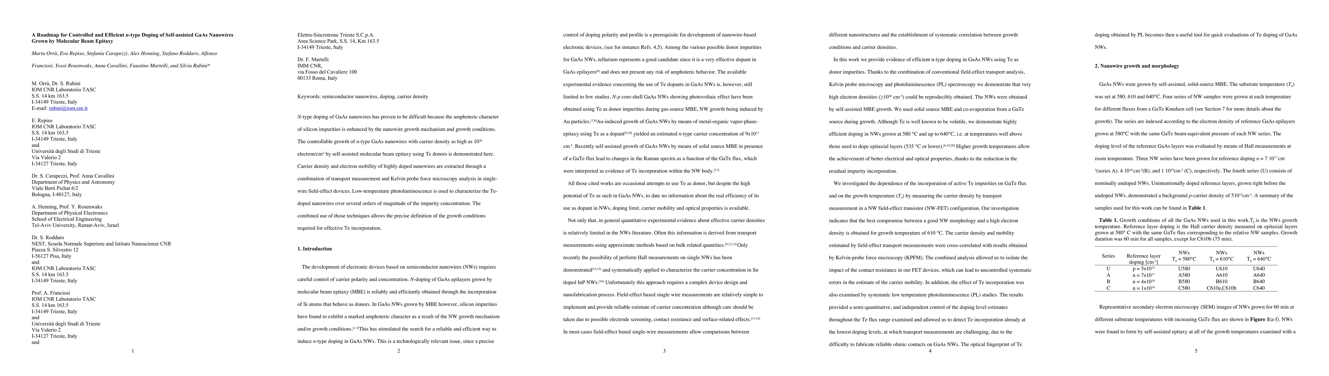
N-type doping of GaAs nanowires has proven to be difficult because the amphoteric character of silicon impurities is enhanced by the nanowire growth mechanism and growth conditions. The controllable...

Thumbnail for Surface NMR using quantum sensors in diamond
arXiv
Surface NMR using quantum sensors in diamond

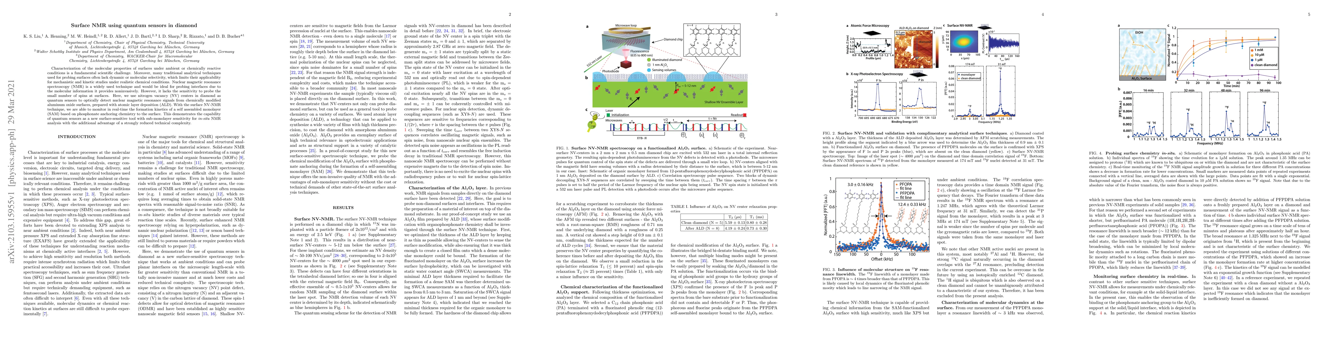
Characterization of the molecular properties of surfaces under ambient or chemically reactive conditions is a fundamental scientific challenge. Moreover, many traditional analytical techniques used ...

Thumbnail for Aluminum Oxide at the Monolayer Limit via Oxidant-free Plasma-Assisted
  Atomic Layer Deposition on GaN
arXiv
Aluminum Oxide at the Monolayer Limit via Oxidant-free Plasma-Assisted Atomic Layer Deposition on GaN

Atomic layer deposition (ALD) is an essential tool in semiconductor device fabrication that allows the growth of ultrathin and conformal films to precisely form heterostructures and tune interface p...

Thumbnail for Atomically Flat Dielectric Patterns for Band Gap Engineering and Lateral
  Junction Formation in MoSe$_2$ Monolayers
arXiv
Atomically Flat Dielectric Patterns for Band Gap Engineering and Lateral Junction Formation in MoSe$_2$ Monolayers

Combining a precise sputter etching method with subsequent AlO$_x$ growth within an atomic layer deposition chamber enables fabrication of atomically flat lateral patterns of SiO$_2$ and AlO$_x$. The ...

This website uses cookies to ensure you get the best experience. Learn more