Academic Profile
Statistics
Similar Authors
Papers on arXiv
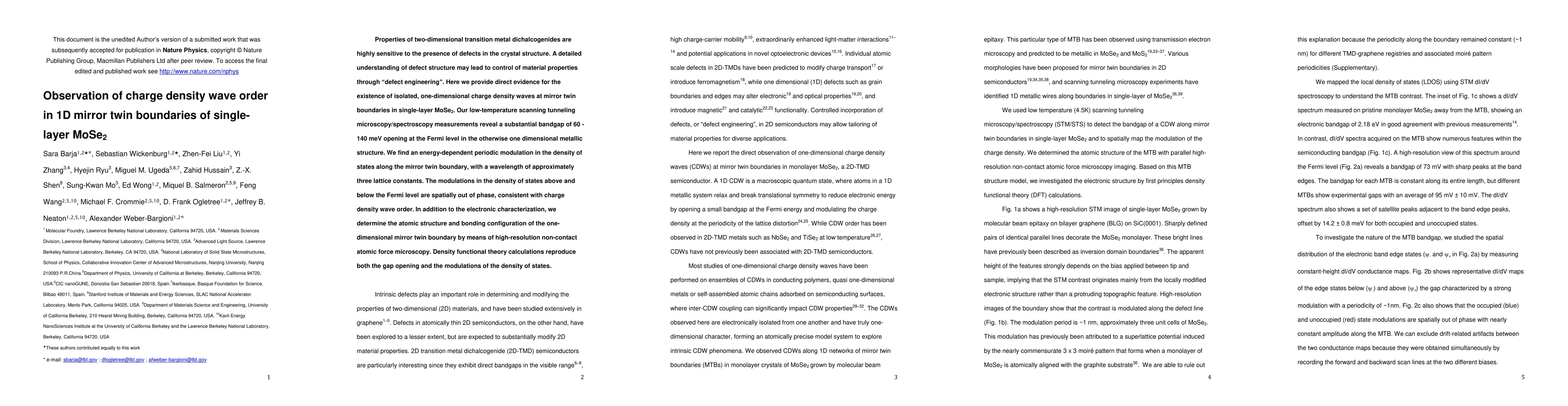
Properties of two-dimensional transition metal dichalcogenides are highly sensitive to the presence of defects in the crystal structure. A detailed understanding of defect structure may lead to cont...
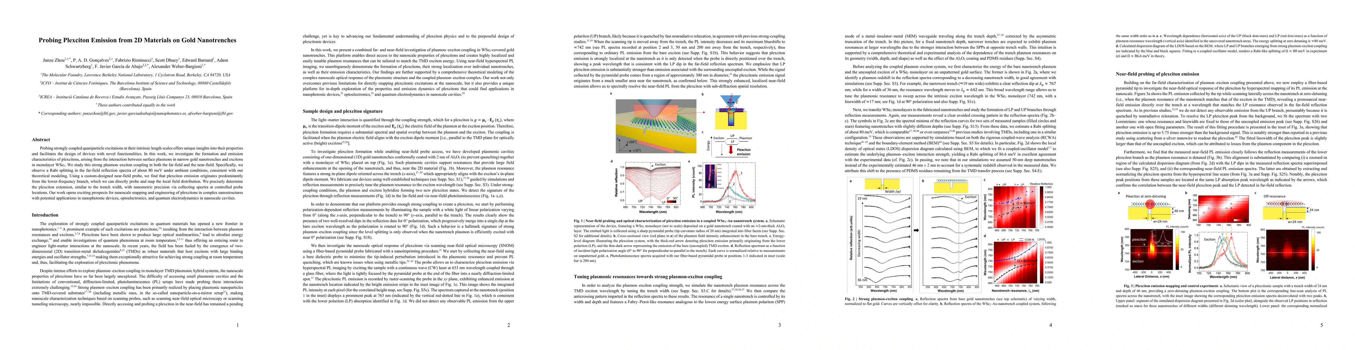
Probing strongly coupled quasiparticle excitations at their intrinsic length scales offers unique insights into their properties and facilitates the design of devices with novel functionalities. In ...
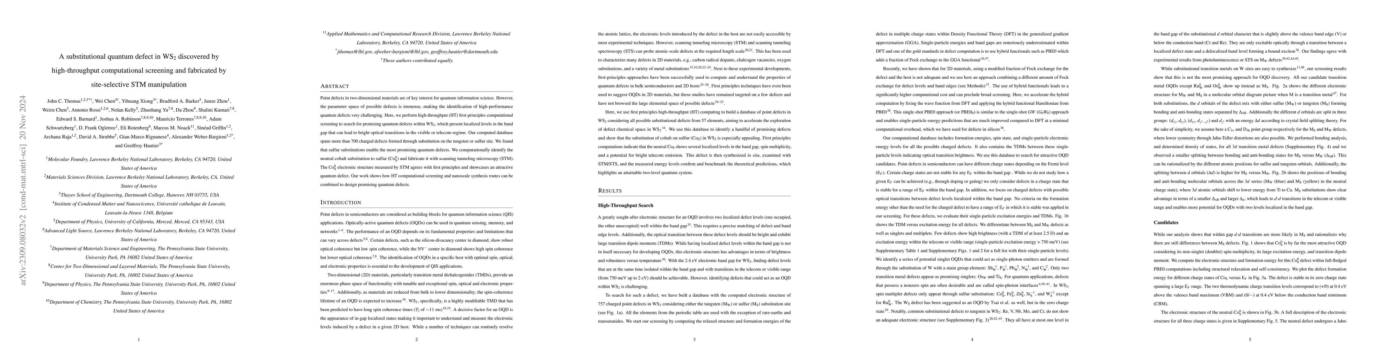
Point defects in two-dimensional materials are of key interest for quantum information science. However, the space of possible defects is immense, making the identification of high-performance quant...
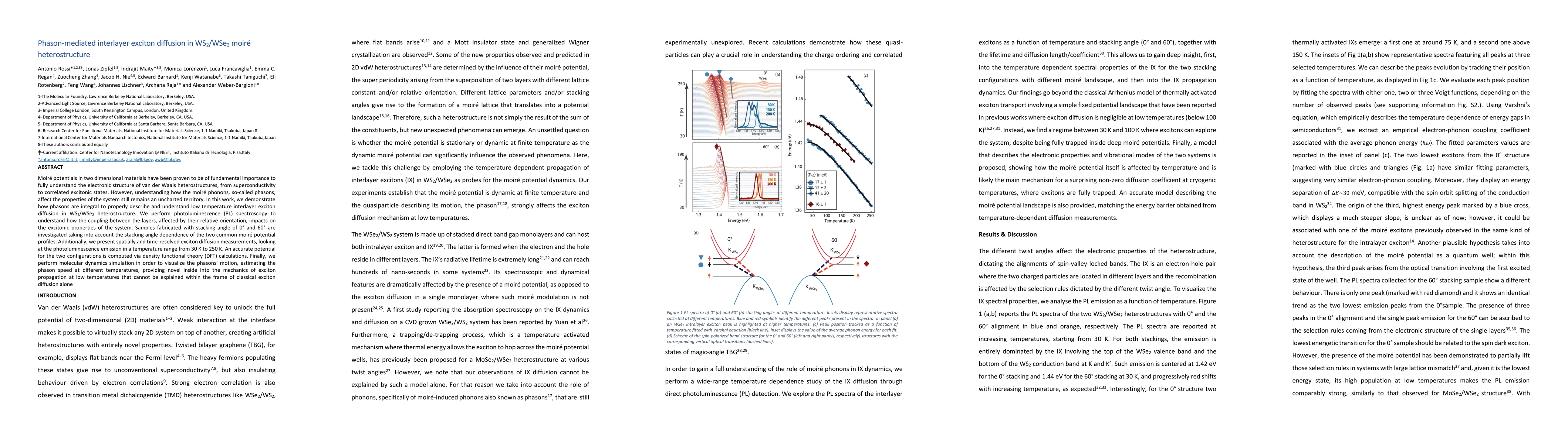
Moir\'e potentials in two-dimensional materials have been proven to be of fundamental importance to fully understand the electronic structure of van der Waals heterostructures, from superconductivit...
Tomonaga-Luttinger liquid (TLL) behavior in one-dimensional systems has been predicted and shown to occur at semiconductor-to-metal transitions within two-dimensional materials. Reports of mirror tw...
Individual atomic defects in 2D materials impact their macroscopic functionality. Correlating the interplay is challenging, however, intelligent hyperspectral scanning tunneling spectroscopy (STS) m...
Quantum sensing and computation can be realized with superconducting microwave circuits. Qubits are engineered quantum systems of capacitors and inductors with non-linear Josephson junctions. They o...
We demonstrate the creation of a spin-1/2 state via the atomically controlled generation of magnetic carbon radical ions (CRIs) in synthetic two-dimensional transition metal dichalcogenides (TMDs). ...
Two-dimensional heterostructures with layers of slightly different lattice vectors exhibit a new periodic structure known as moire lattices. Moire lattice formation provides a powerful new way to en...
Control of impurity concentrations in semiconducting materials is essential to device technology. Because of their intrinsic confinement, the properties of two-dimensional semiconductors such as tra...
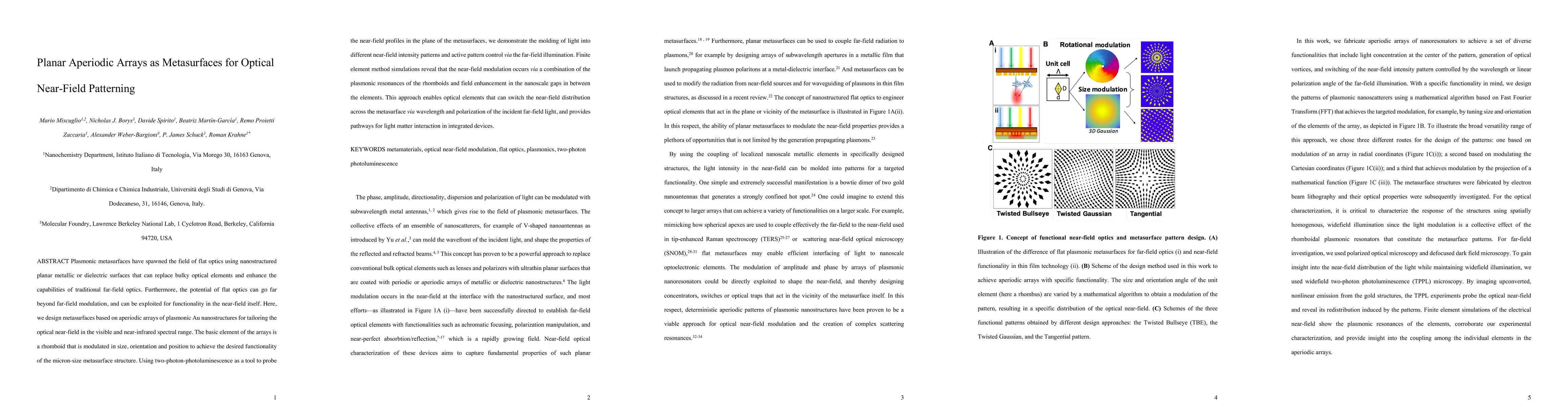
Plasmonic metasurfaces have spawned the field of flat optics using nanostructured planar metallic or dielectric surfaces that can replace bulky optical elements and enhance the capabilities of tradi...
Bilayer graphene was theorized to host a moire miniband with flat dispersion if the layers are stacked at specific twist angles known as the magic angles. Recently, such twisted bilayer graphene (tB...
Optical quantum emitters are a key component of quantum devices for metrology and information processing. In particular, atomic defects in 2D materials can operate as optical quantum emitters that o...
A detailed understanding of charged defects in two-dimensional semiconductors is needed for the development of ultrathin electronic devices. Here, we study negatively charged acceptor impurities in ...
Excitons in 2D material bubbles-nanoscale deformations in atomically thin materials, typically exhibiting a dome-like shape-are confined by the strain effect, exhibiting extraordinary emission propert...
Chalcogen vacancies in monolayer transition metal dichalcogenides (TMDs), such as WS$_{2}$, play a crucial role in various applications ranging from optoelectronics and catalysis to quantum informatio...