Academic Profile
Statistics
Similar Authors
Papers on arXiv
Classic Delphi and Fuzzy Delphi methods are used to test content validity of a data collection tools such as questionnaires. Fuzzy Delphi takes the opinion issued by judges from a linguistic perspec...
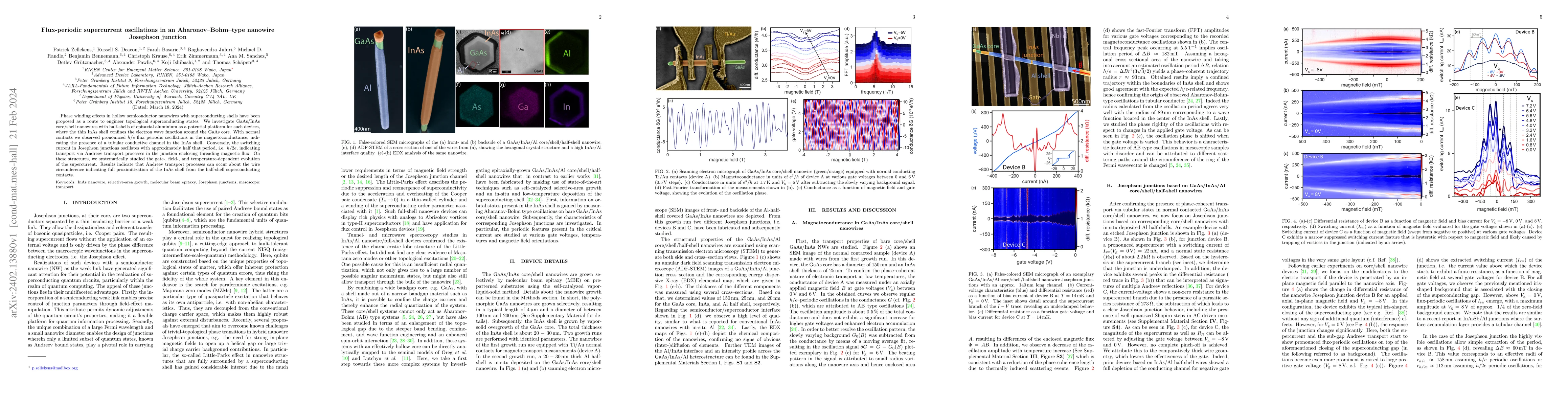
Phase winding effects in hollow semiconductor nanowires with superconducting shells have been proposed as a route to engineer topological superconducting states. We investigate GaAs/InAs core/shell ...
Incorporation of Bi into GaAs-(Ga,Al)As-Ga(As,Bi) core-shell nanowires grown by molecular beam epitaxy is studied with transmission electron microscopy. Nanowires are grown on GaAs(111)B substrates ...
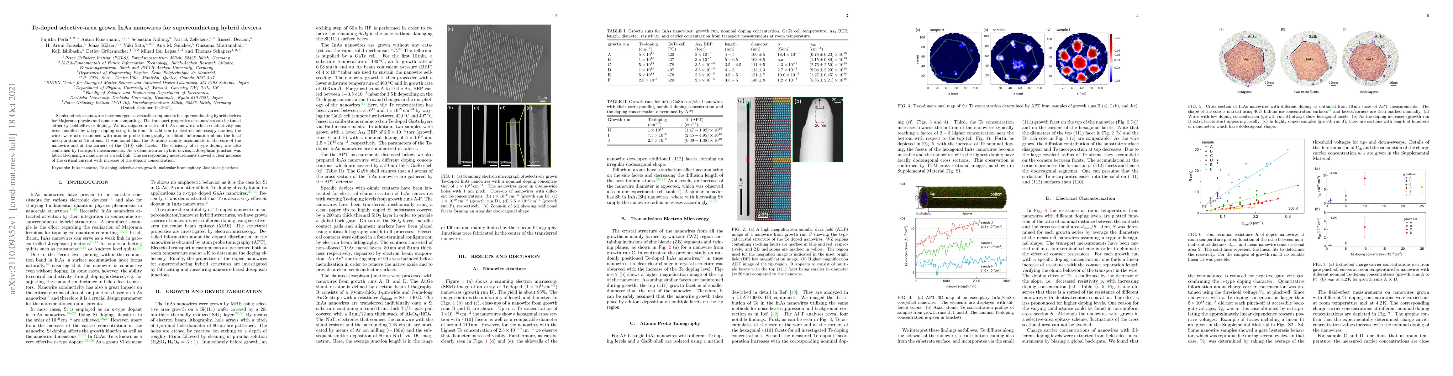
Semiconductor nanowires have emerged as versatile components in superconducting hybrid devices for Majorana physics and quantum computing. The transport properties of nanowires can be tuned either b...
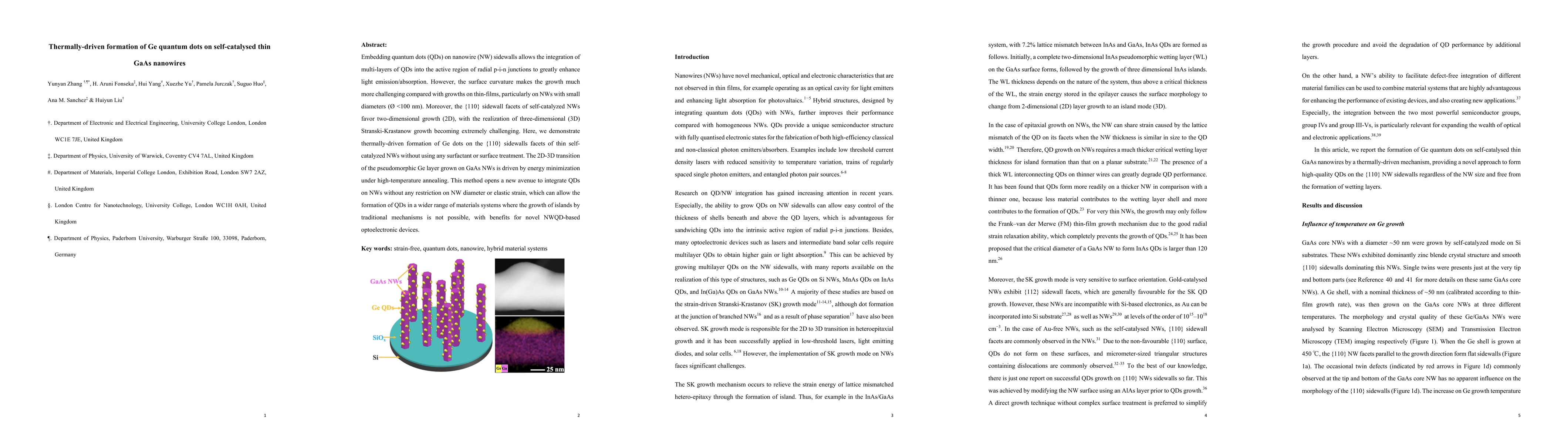
Embedding quantum dots (QDs) on nanowire (NW) sidewalls allows the integration of multi-layers of QDs into the active region of radial p-i-n junctions to greatly enhance light emission/absorption. H...
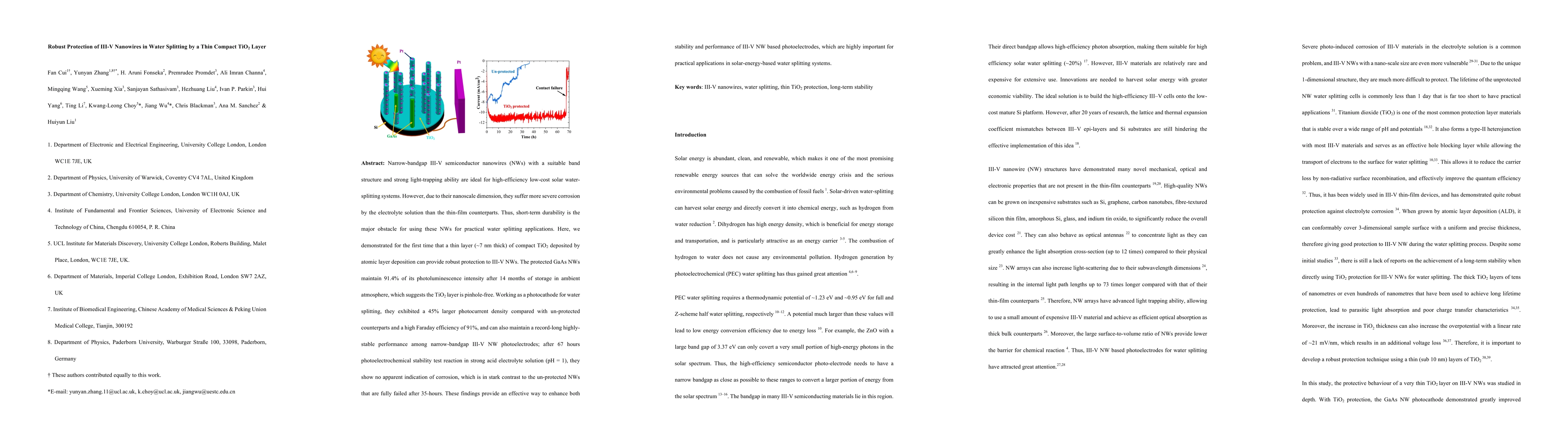
Narrow-bandgap III-V semiconductor nanowires (NWs) with a suitable band structure and strong light-trapping ability are ideal for high-efficiency low-cost solar water-splitting systems. However, due...
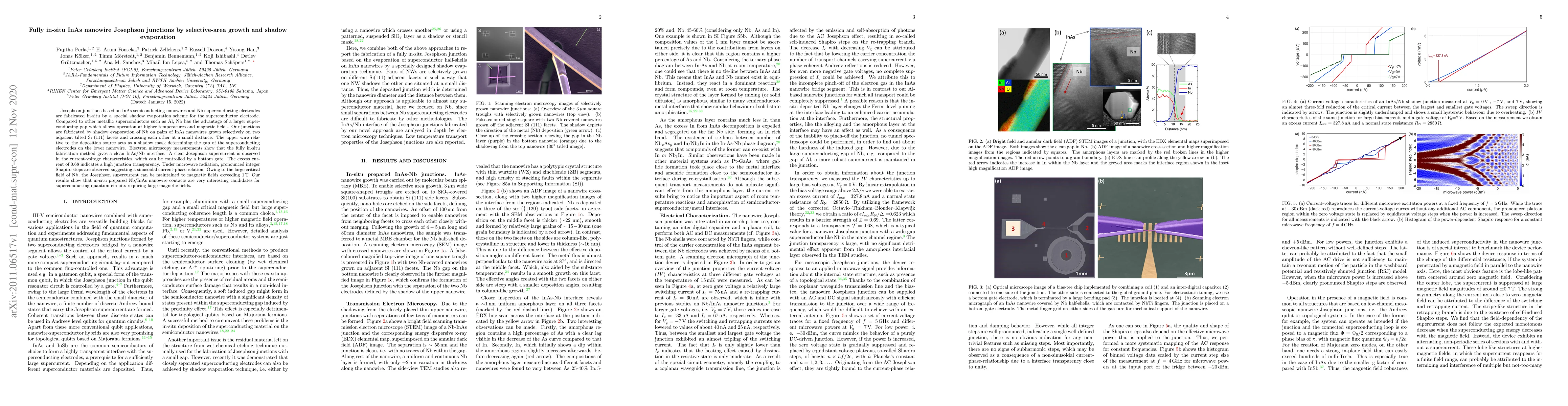
Josephson junctions based on InAs semiconducting nanowires and Nb superconducting electrodes are fabricated in-situ by a special shadow evaporation scheme for the superconductor electrode. Compared ...
Alloying enables engineering of the electronic structure of semiconductors for optoelectronic applications. Due to their similar lattice parameters, the two-dimensional semiconducting transition met...
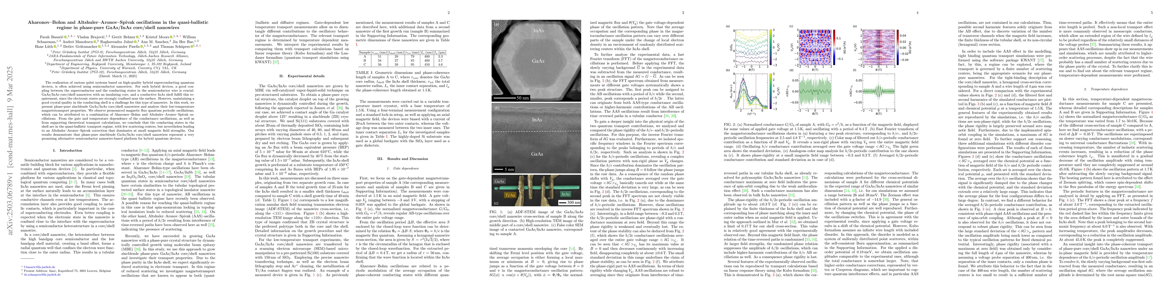
The realization of various qubit systems based on high-quality hybrid superconducting quantum devices, is often achieved using semiconductor nanowires. For such hybrid devices, a good coupling between...
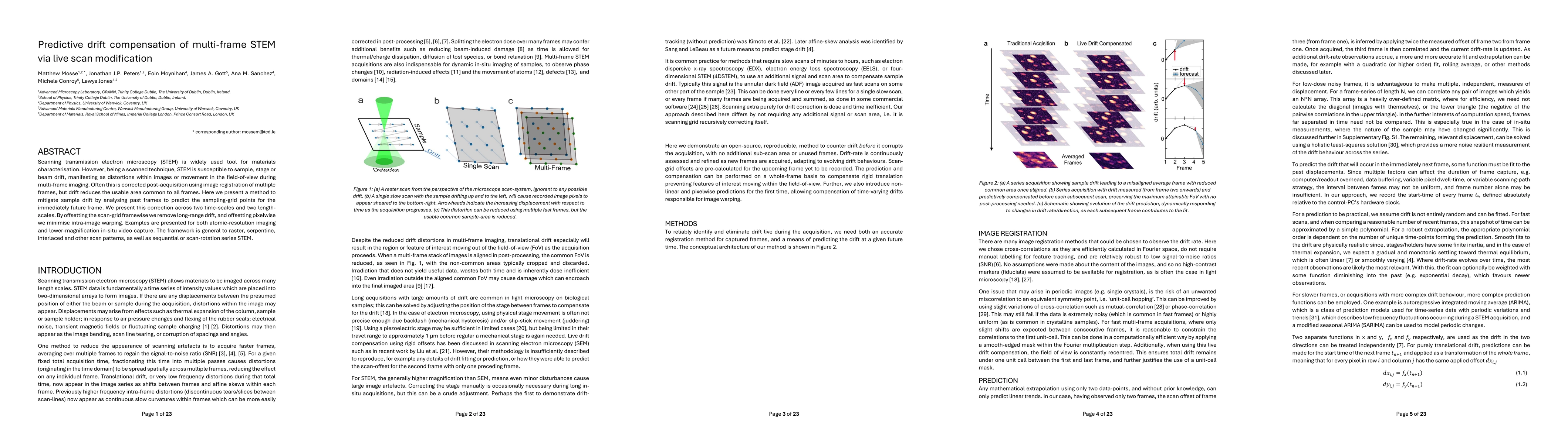
Scanning transmission electron microscopy (STEM) is widely used tool for materials characterisation. However, being a scanned technique, STEM is susceptible to sample, stage or beam drift, manifesting...
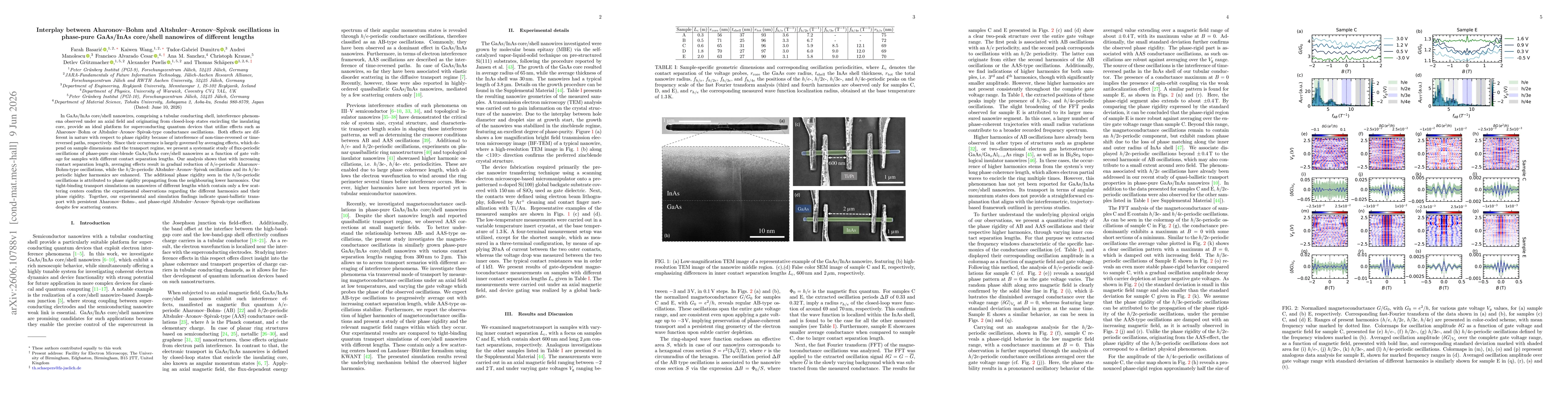
In GaAs/InAs core/shell nanowires, comprising a tubular conducting shell, interference phenomena observed under an axial field and originating from closed-loop states encircling the insulating core, p...