Academic Profile
Statistics
Similar Authors
Papers on arXiv
The Nernst effect, a transverse thermoelectric phenomenon, has attracted significant attention for its potential in energy conversion, thermoelectrics, and spintronics. However, achieving high perfo...
Adapting electronics to perfectly conform to non-planar and rough surfaces, such as human skin, is a very challenging task which, if solved, could open up new applications in fields of high economic...
Two-dimensional flat-band systems have recently attracted considerable interest due to the rich physics unveiled by emergent phenomena and correlated electronic states at van Hove singularities. How...
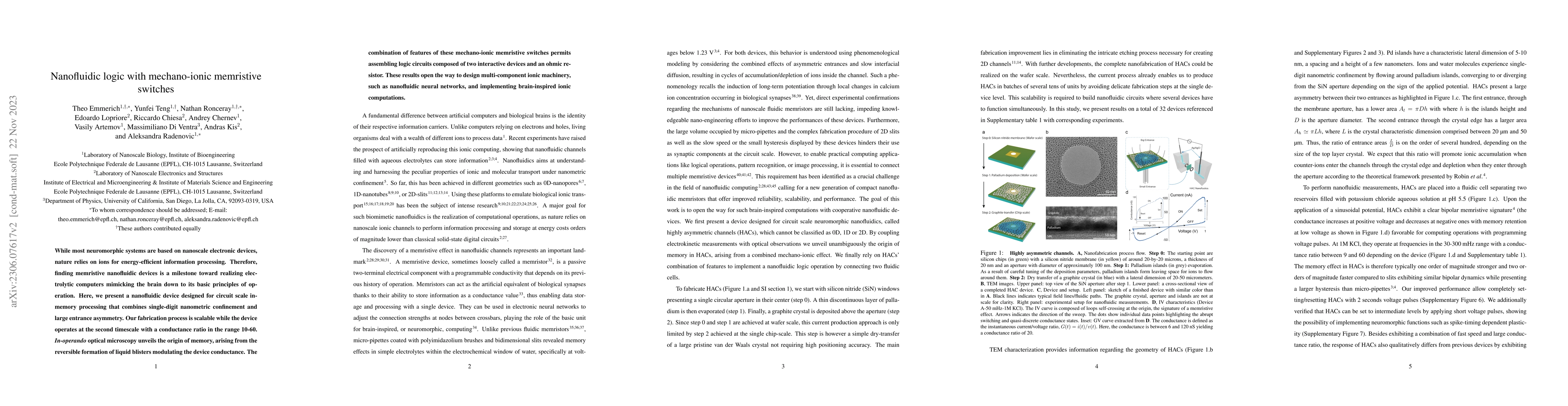
While most neuromorphic systems are based on nanoscale electronic devices, nature relies on ions for energy-efficient information processing. Therefore, finding memristive nanofluidic devices is a m...
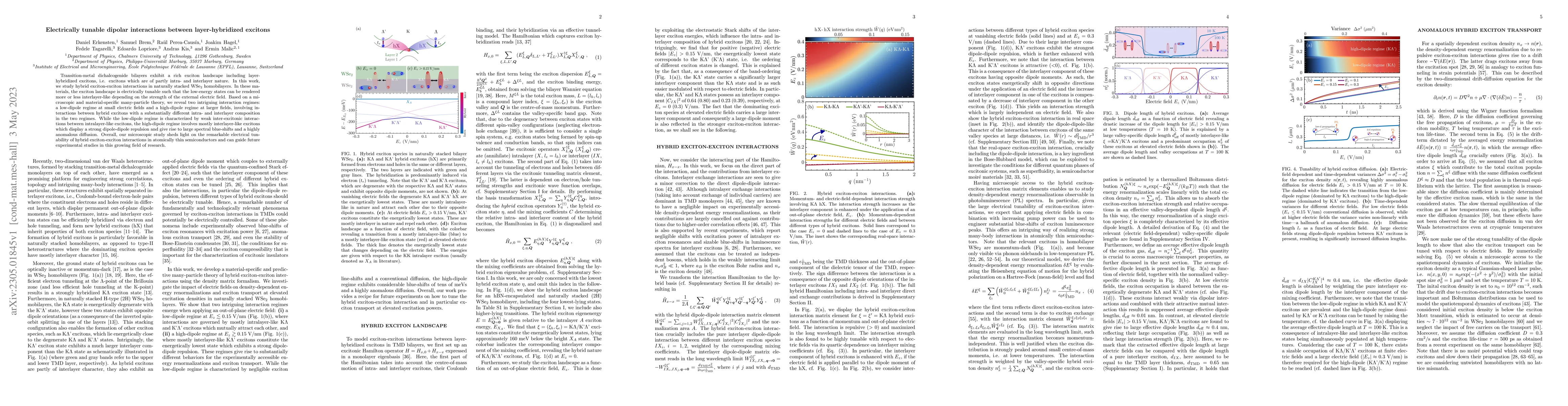
Transition-metal dichalcogenide bilayers exhibit a rich exciton landscape including layer-hybridized excitons, i.e. excitons which are of partly intra- and interlayer nature. In this work, we study ...
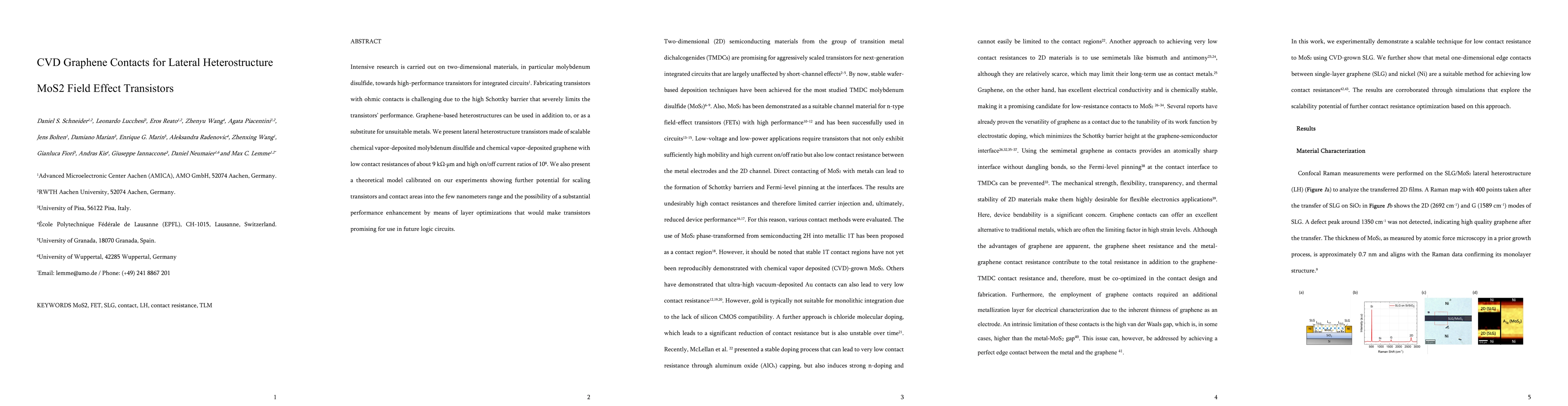
Intensive research is carried out on two-dimensional materials, in particular molybdenum disulfide, towards high-performance transistors for integrated circuits. Fabricating transistors with ohmic c...
Led by the rise of the internet of things, the world is experiencing exponential growth of generated data. Data-driven algorithms such as signal processing and artificial neural networks are require...
Interactions between out-of-plane dipoles in bosonic gases enable the long-range propagation of excitons. The lack of direct control over collective dipolar properties has hitherto limited the degre...
Interactions among a collection of particles generate many-body effects in solids resulting in striking modifications of material properties. The heavy carrier mass that yields strong interactions a...
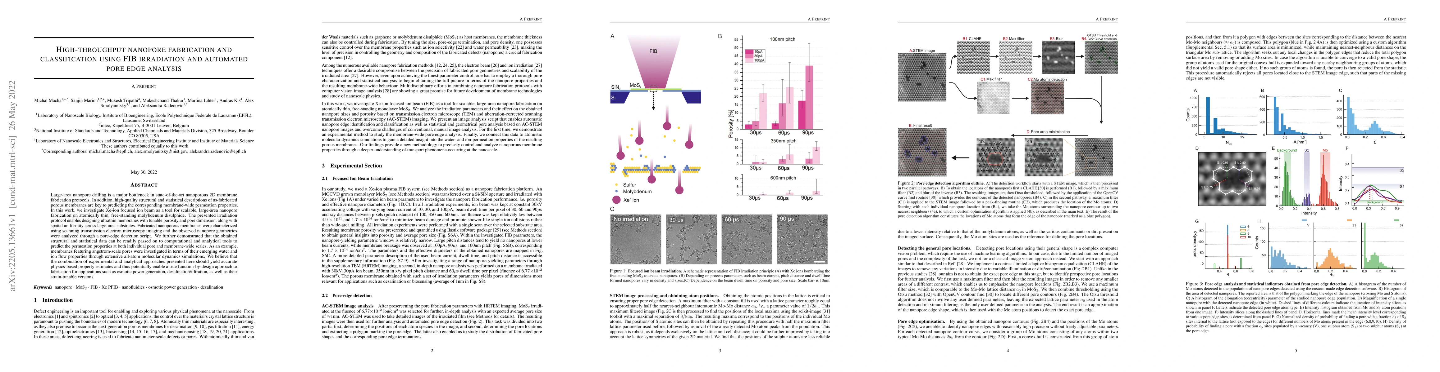
Large-area nanopore drilling is a major bottleneck in state-of-the-art nanoporous 2D membrane fabrication protocols. In addition, high-quality structural and statistical descriptions of as-fabricate...
We demonstrate the design, fabrication, and characterization of wafer-scale, zero-bias power detectors based on two-dimensional MoS$_2$ field effect transistors (FETs). The MoS$_2$ FETs are fabricat...
Dipolar bosonic gases are currently the focus of intensive research due to their interesting many-body physics in the quantum regime. Their experimental embodiments range from Rydberg atoms to GaAs ...
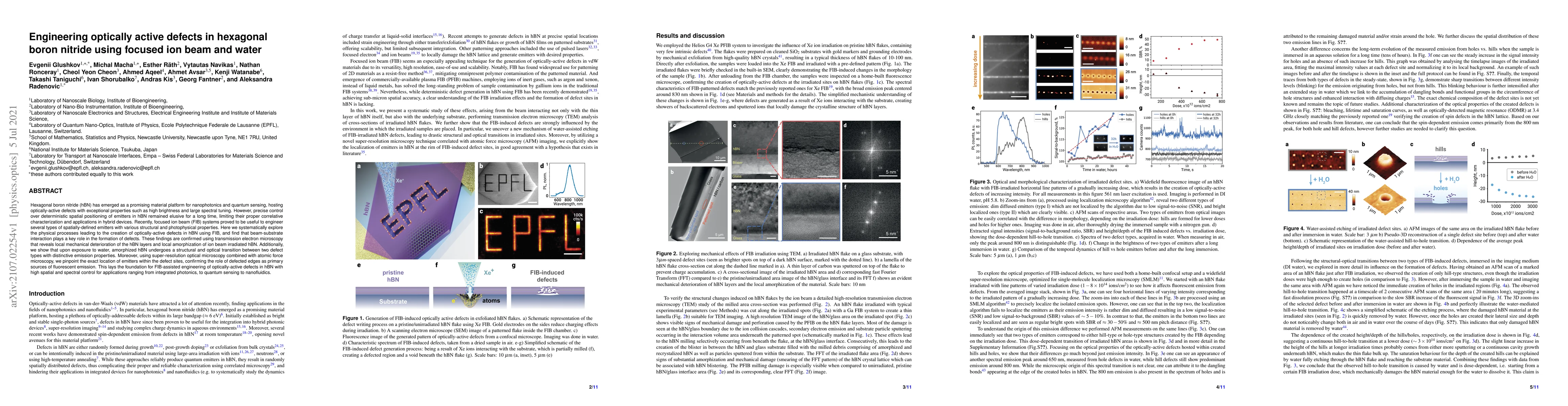
Hexagonal boron nitride (hBN) has emerged as a promising material platform for nanophotonics and quantum sensing, hosting optically-active defects with exceptional properties such as high brightness...

Transition metal dichalcogenides (TMDs) represent an entire new class of semiconducting 2D materials with exciting properties. Defects in 2D TMDs can crucially affect their physical and chemical pro...
Long-lived interlayer excitons with distinct spin-valley physics in van der Waals heterostructures based on transition metal dichalcogenides make them promising for information processing in next-ge...
Extended efforts have been devoted to the study of strongly-interacting excitons and their dynamics, towards macroscopic quantum states of matter such as Bose-Einstein condensates of excitons and pola...
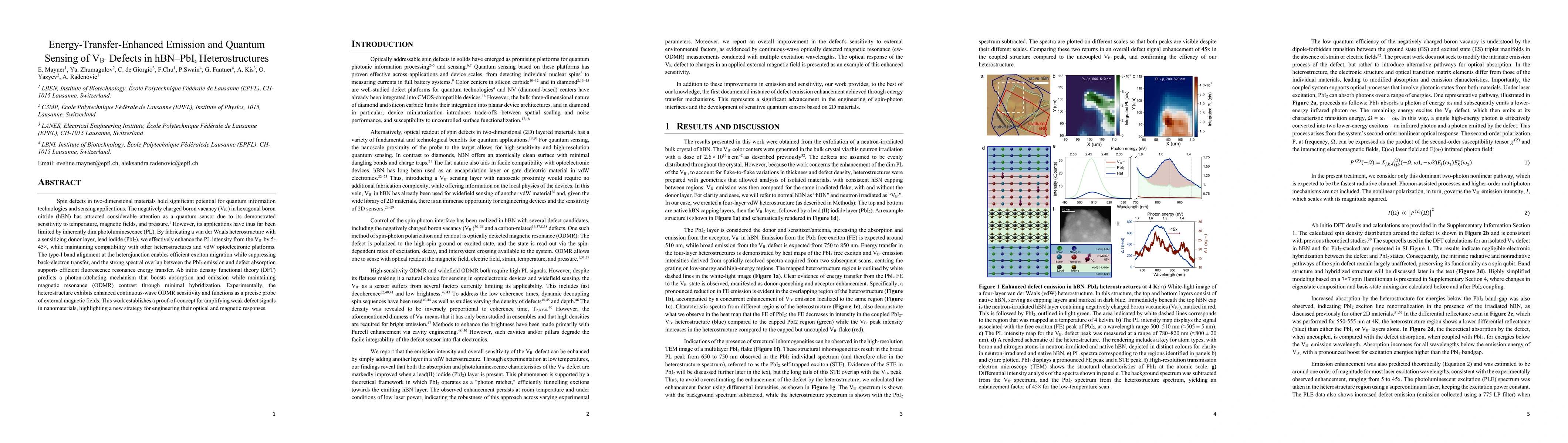
Spin defects in two-dimensional materials hold significant potential for quantum information technologies and sensing applications. The negatively charged boron vacancy (VB-) in hexagonal boron nitrid...
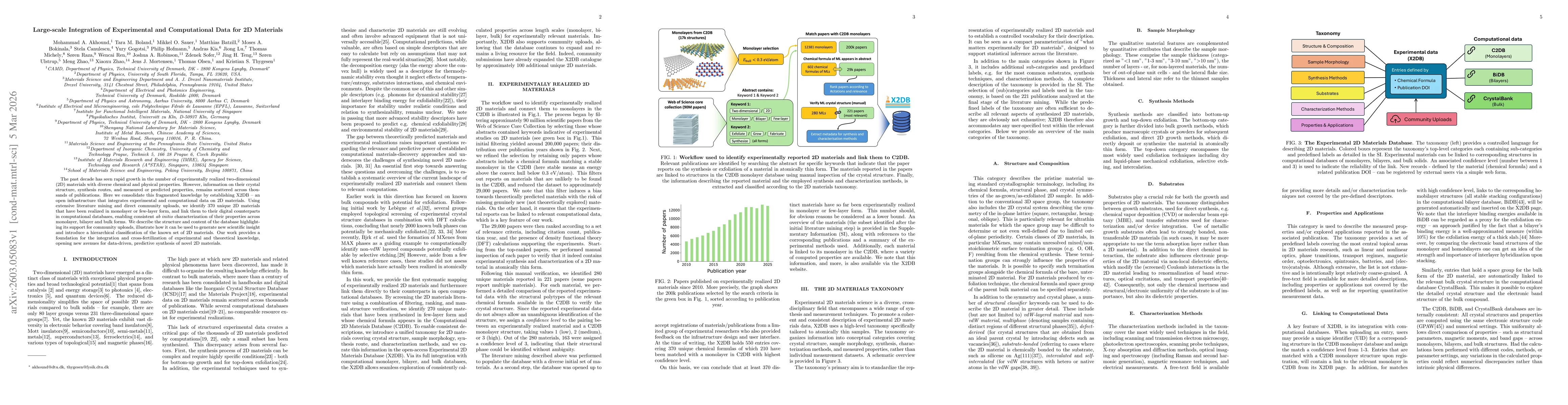
The past decade has seen rapid growth in the number of experimentally realized two-dimensional (2D) materials with diverse chemical and physical properties. However, information on their crystal struc...