Academic Profile
Statistics
Similar Authors
Papers on arXiv
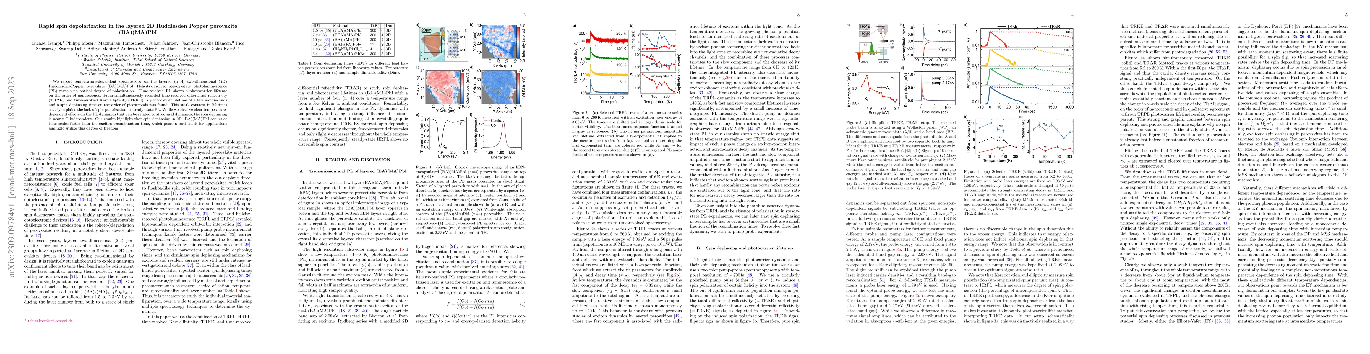
We report temperature-dependent spectroscopy on the layered (n=4) two-dimensional (2D) Ruddlesden-Popper perovskite (BA)(MA)PbI. Helicity-resolved steady-state photoluminescence (PL) reveals no opti...
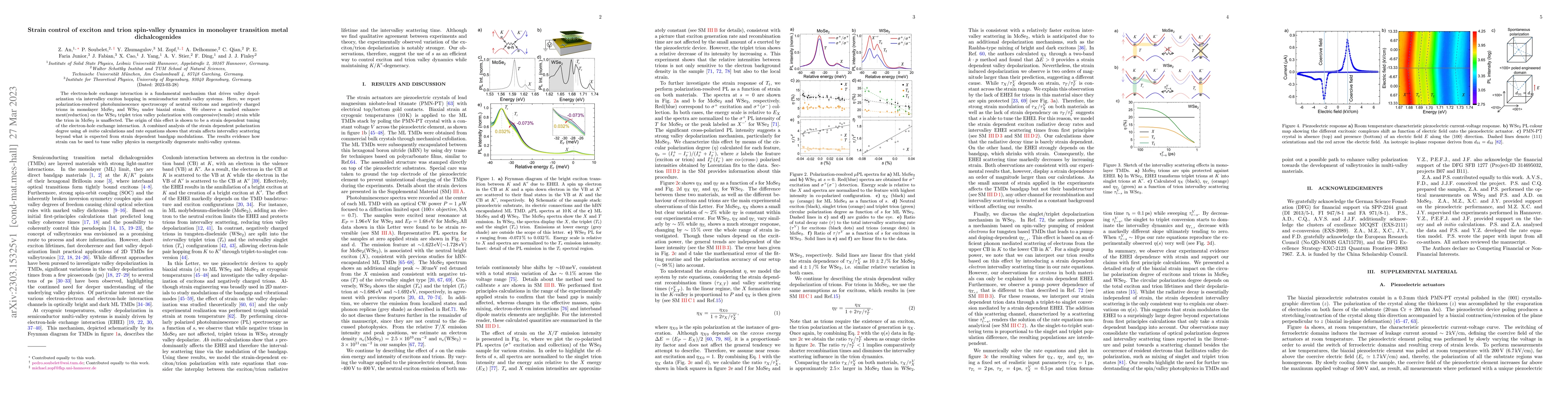
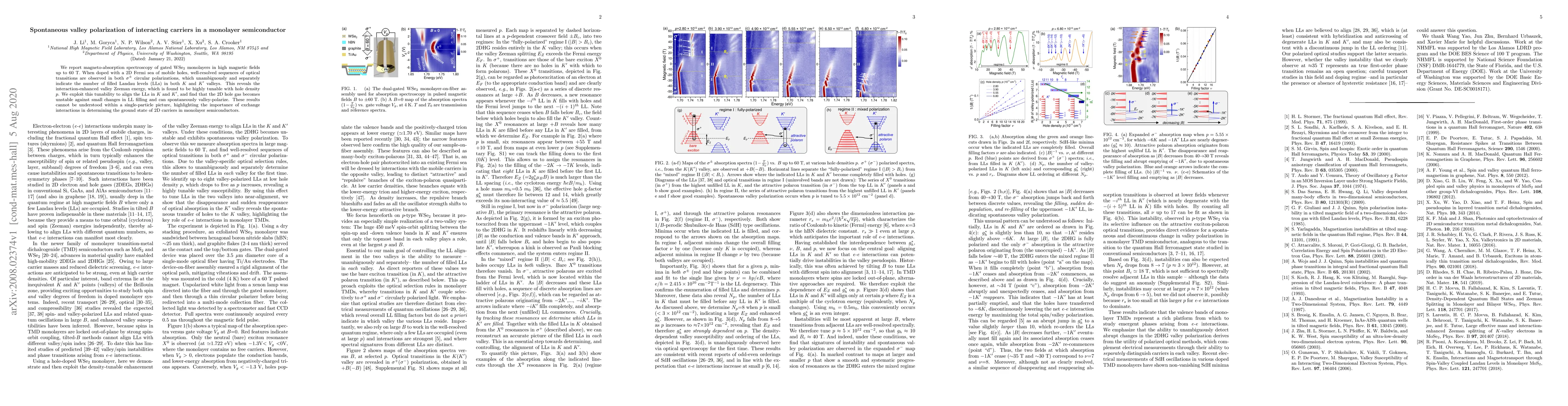
The electron-hole exchange interaction is a fundamental mechanism that drives valley depolarization via intervalley exciton hopping in semiconductor multi-valley systems. Here, we report polarizatio...
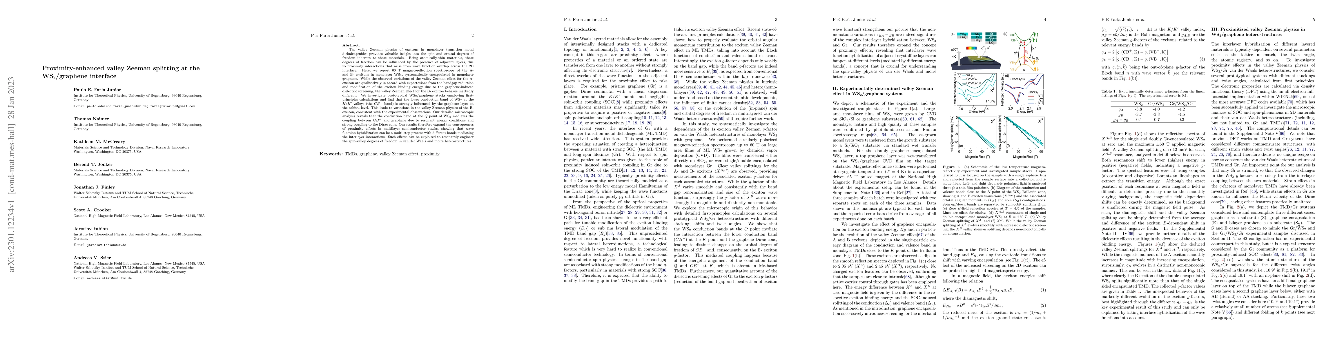
The valley Zeeman physics of excitons in monolayer transition metal dichalcogenides provides valuable insight into the spin and orbital degrees of freedom inherent to these materials. Being atomical...
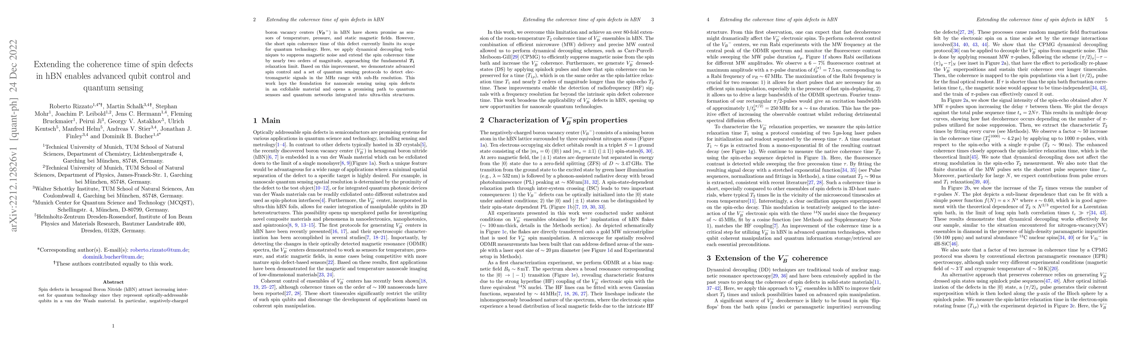
Spin defects in hexagonal Boron Nitride (hBN) attract increasing interest for quantum technology since they represent optically-addressable qubits in a van der Waals material. In particular, negativ...
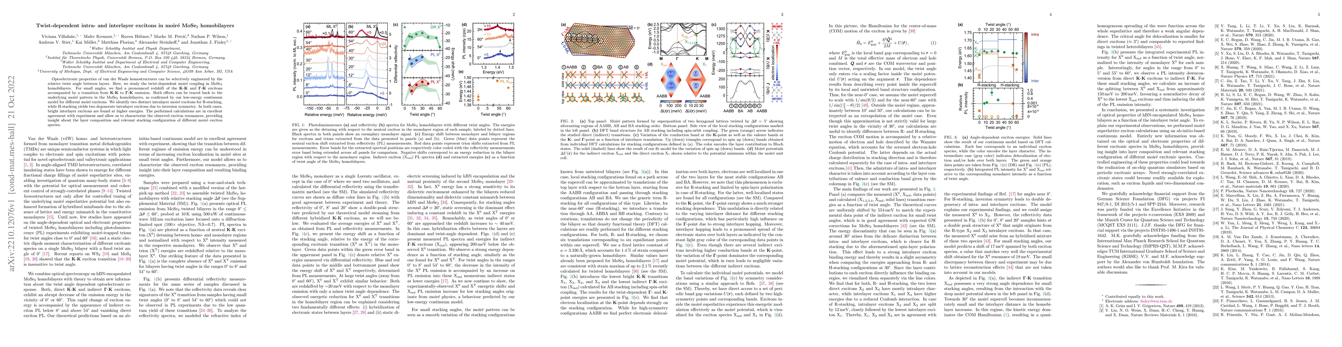
Optoelectronic properties of van der Waals homostructures can be selectively engineered by the relative twist angle between layers. Here, we study the twist-dependent moire coupling in MoSe2 homobil...
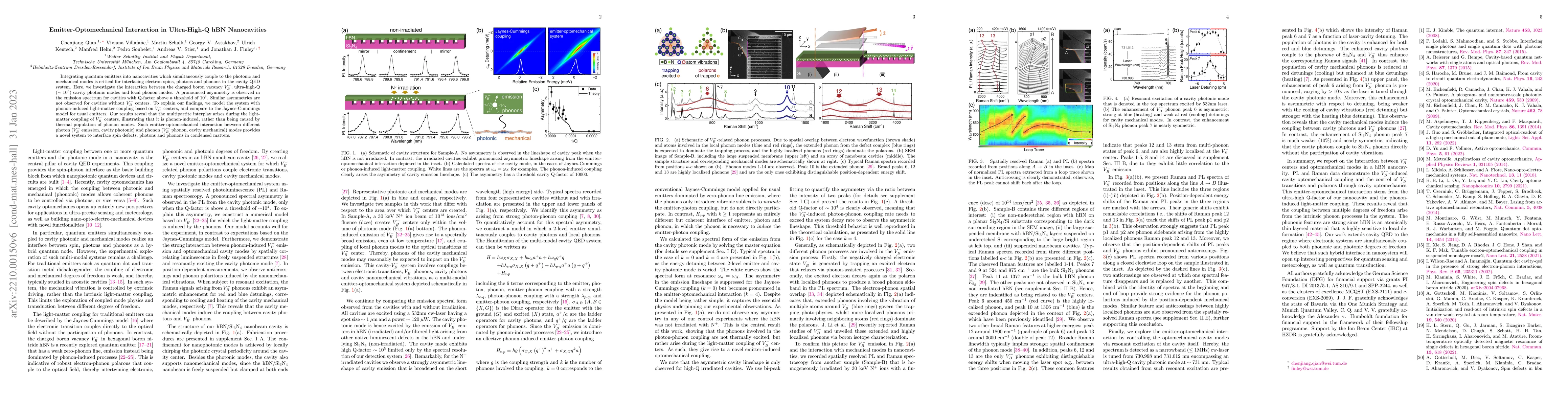
Integrating quantum emitters into nanocavities which simultaneously couple to the photonic and mechanical modes is critical for interfacing electron spins, photons and phonons in the cavity QED syst...
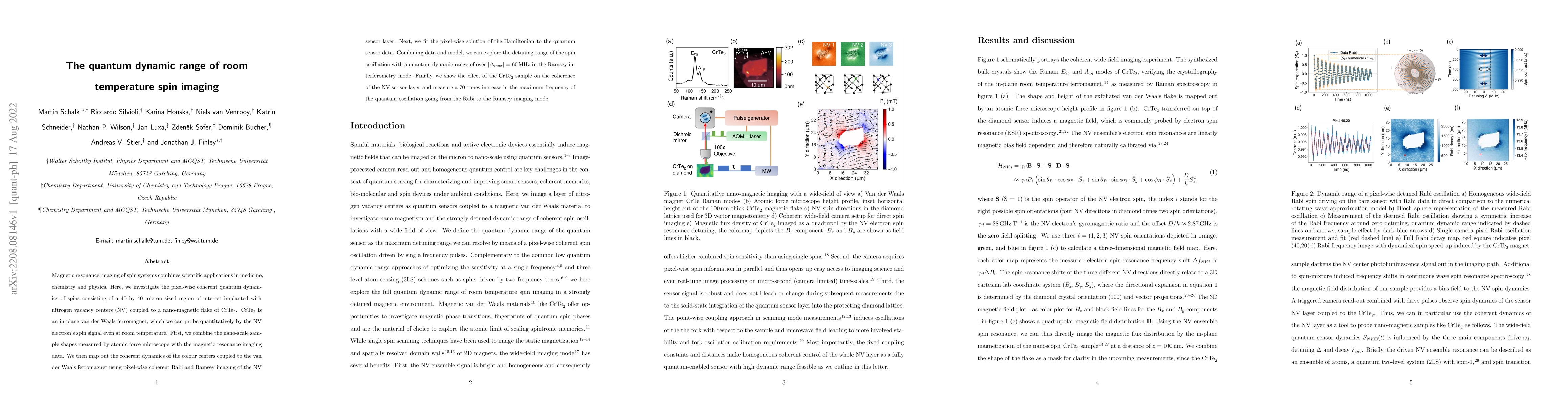
Magnetic resonance imaging of spin systems combines scientific applications in medicine, chemistry and physics. Here, we investigate the pixel-wise coherent quantum dynamics of spins consisting of a...
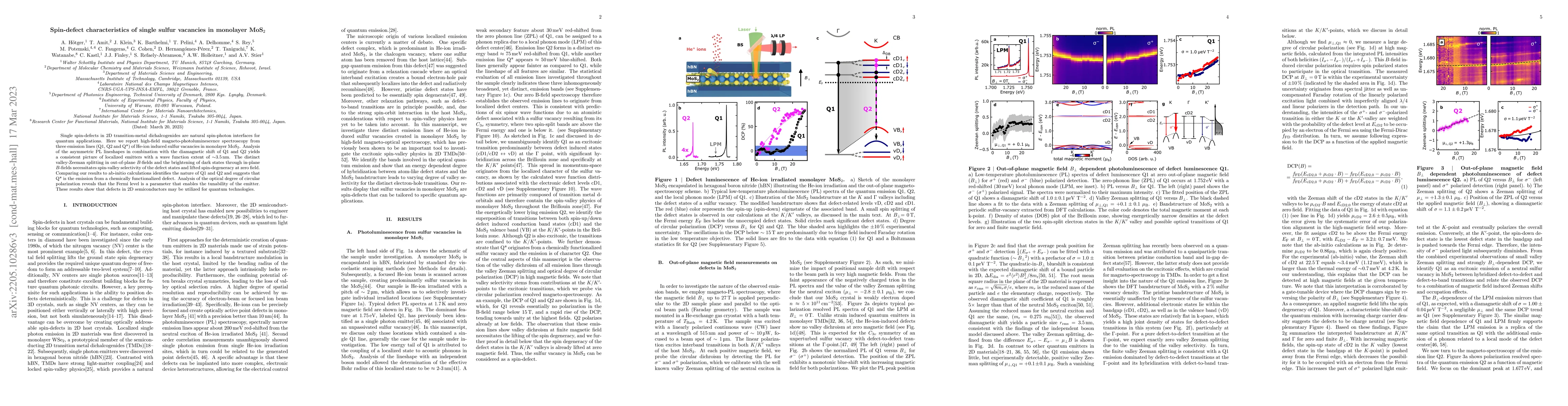
Single spin defects in 2D transition-metal dichalcogenides are natural spin-photon interfaces for quantum applications. Here we report high-field magneto-photoluminescence spectroscopy from three em...
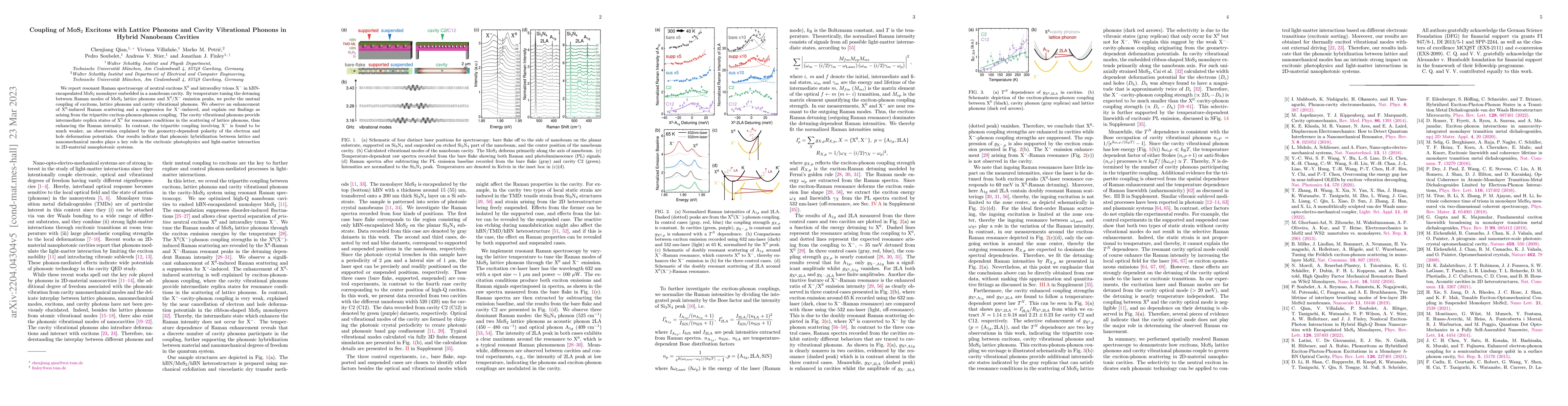
We report resonant Raman spectroscopy of neutral excitons X$^0$ and intravalley trions X$^-$ in hBN-encapsulated MoS$_2$ monolayer embedded in a nanobeam cavity. By temperature tuning the detuning b...
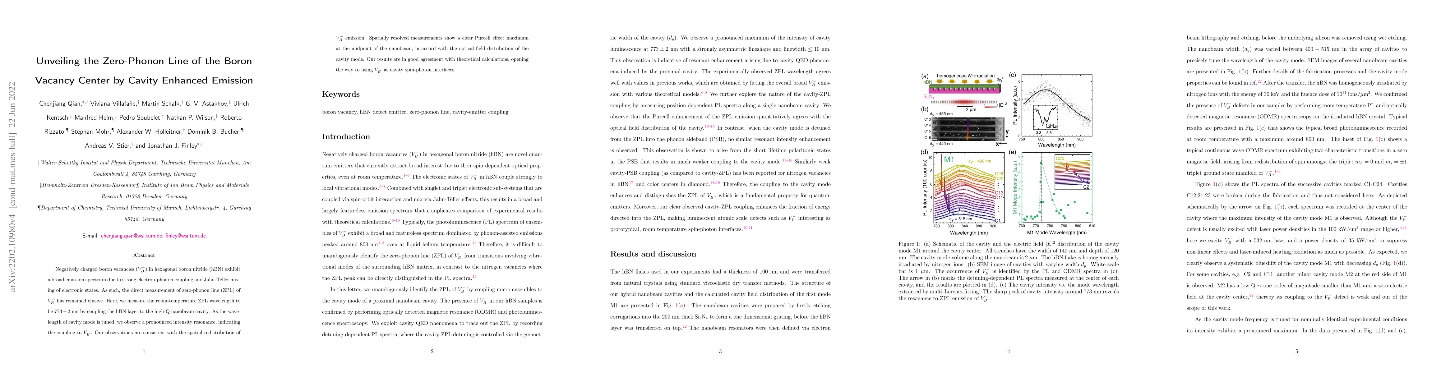
Negatively charged boron vacancies ($V_B^-$) in hexagonal boron nitride (hBN) exhibit a broad emission spectrum due to strong electron-phonon coupling and Jahn-Teller mixing of electronic states. As...
We present a novel transparent conductive support structure for two-dimensional (2D) materials that provides an electronically passive 2D/3D interface while also enabling facile interfacial charge t...
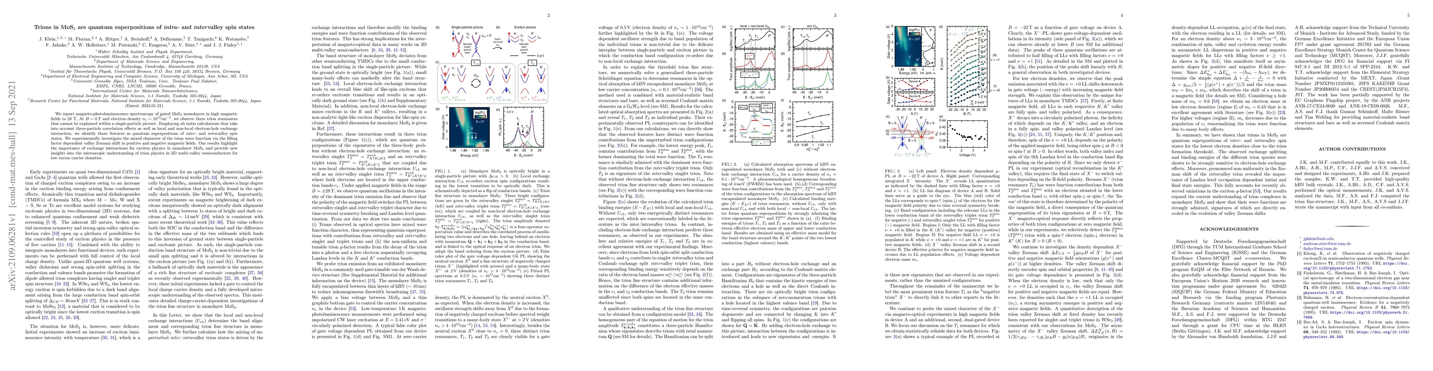
We report magneto-photoluminescence spectroscopy of gated MoS$_2$ monolayers in high magnetic fields to 28 T. At B = 0T and electron density $n_s\sim 10^{12}cm^-2$, we observe three trion resonances...
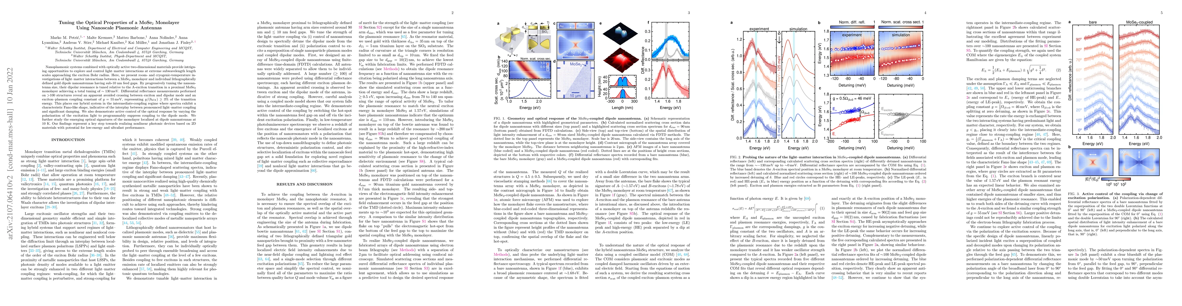
Nanoplasmonic systems combined with optically-active two-dimensional materials provide intriguing opportunities to explore and control light-matter interactions at extreme sub-wavelength lengthscale...
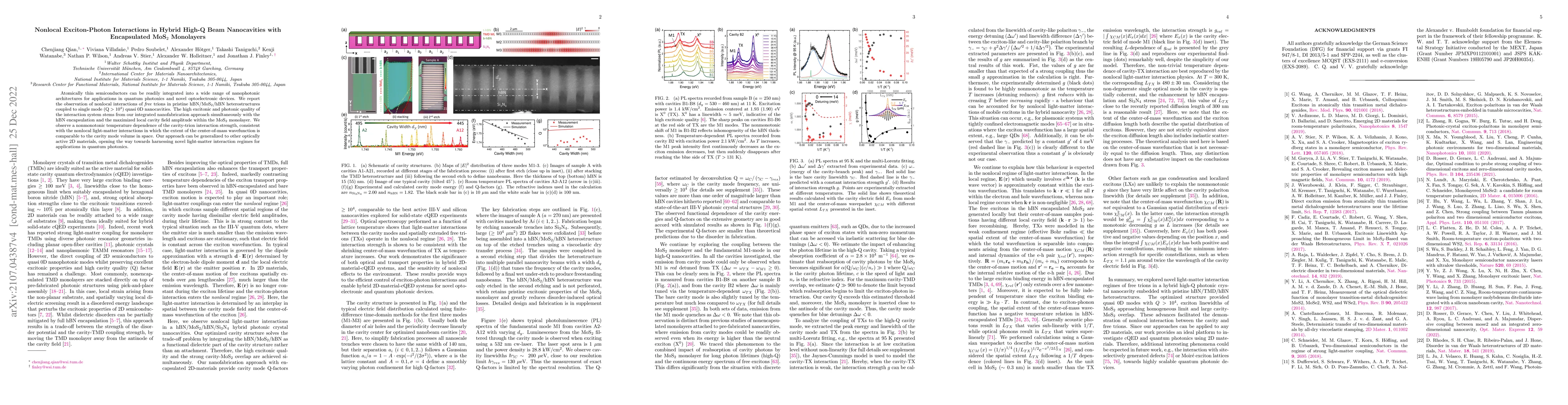
Atomically thin semiconductors can be readily integrated into a wide range of nanophotonic architectures for applications in quantum photonics and novel optoelectronic devices. We report the observa...
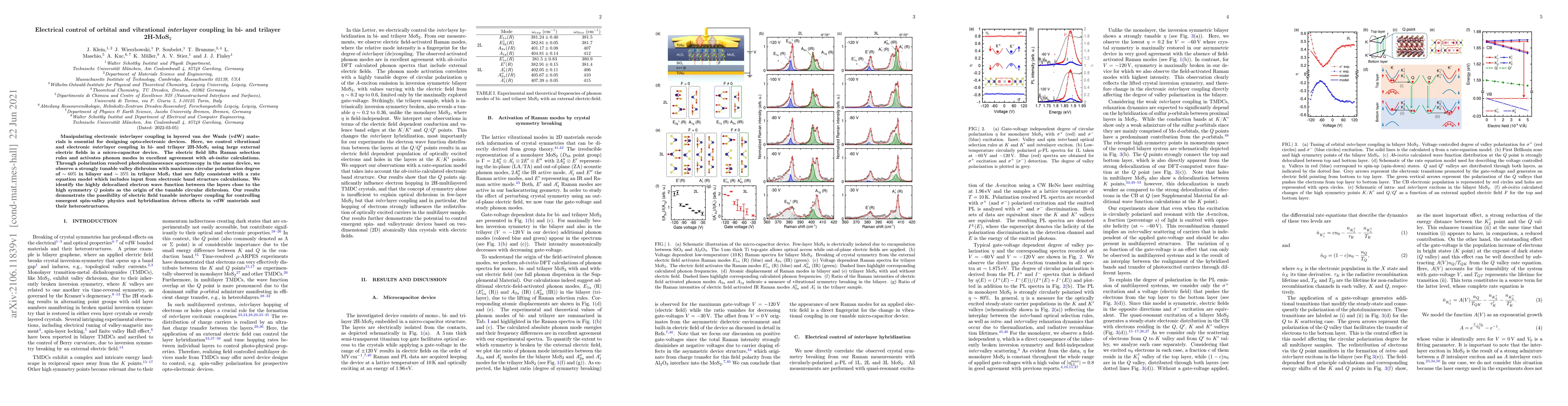
Manipulating electronic interlayer coupling in layered van der Waals (vdW) materials is essential for designing opto-electronic devices. Here, we control vibrational and electronic interlayer coupli...
Monolayers of semiconducting transition metal dichalcogenides are a strongly emergent platform for exploring quantum phenomena in condensed matter, building novel opto-electronic devices with enhanc...
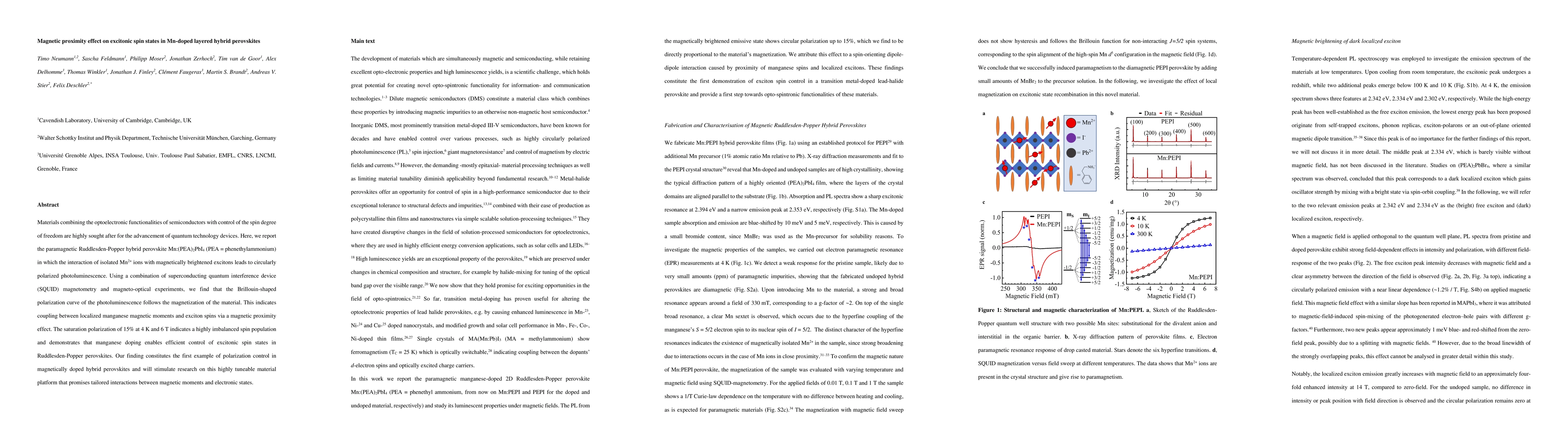
Materials combining the optoelectronic functionalities of semiconductors with control of the spin degree of freedom are highly sought after for the advancement of quantum technology devices. Here, w...
We report magneto-absorption spectroscopy of gated WSe$_2$ monolayers in high magnetic fields up to 60~T. When doped with a 2D Fermi sea of mobile holes, well-resolved sequences of optical transitio...
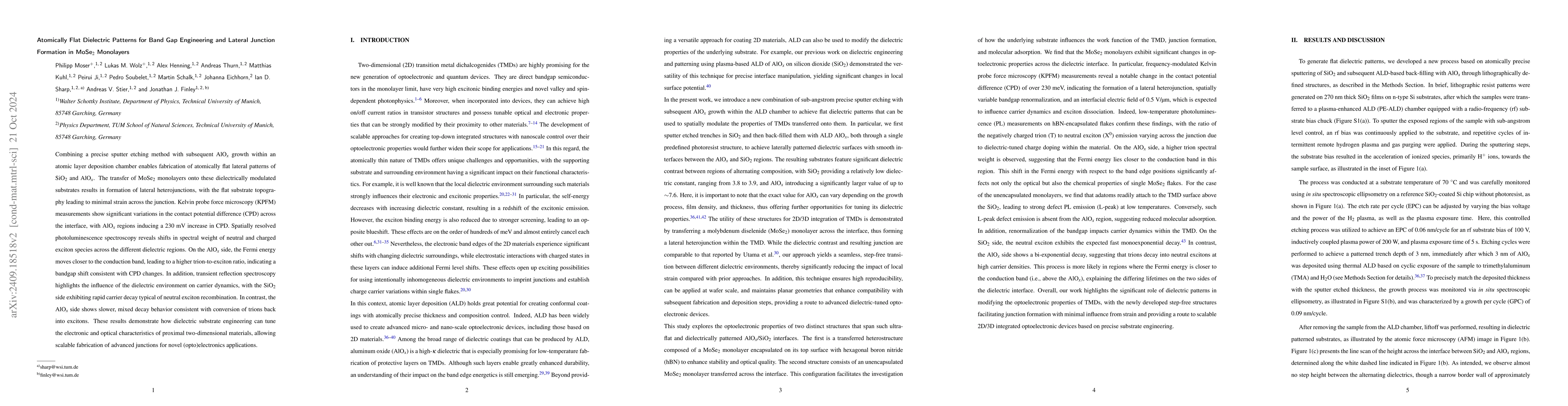
Combining a precise sputter etching method with subsequent AlO$_x$ growth within an atomic layer deposition chamber enables fabrication of atomically flat lateral patterns of SiO$_2$ and AlO$_x$. The ...
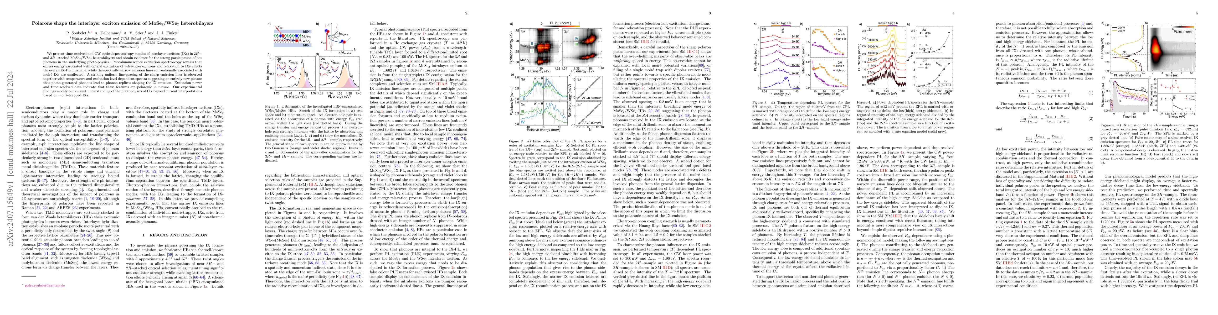
We present time-resolved and CW optical spectroscopy studies of interlayer excitons (IXs) in 2$H-$ and 3$R-$stacked MoSe$_2$/WSe$_2$ heterobilayers and obtain evidence for the strong participation of ...
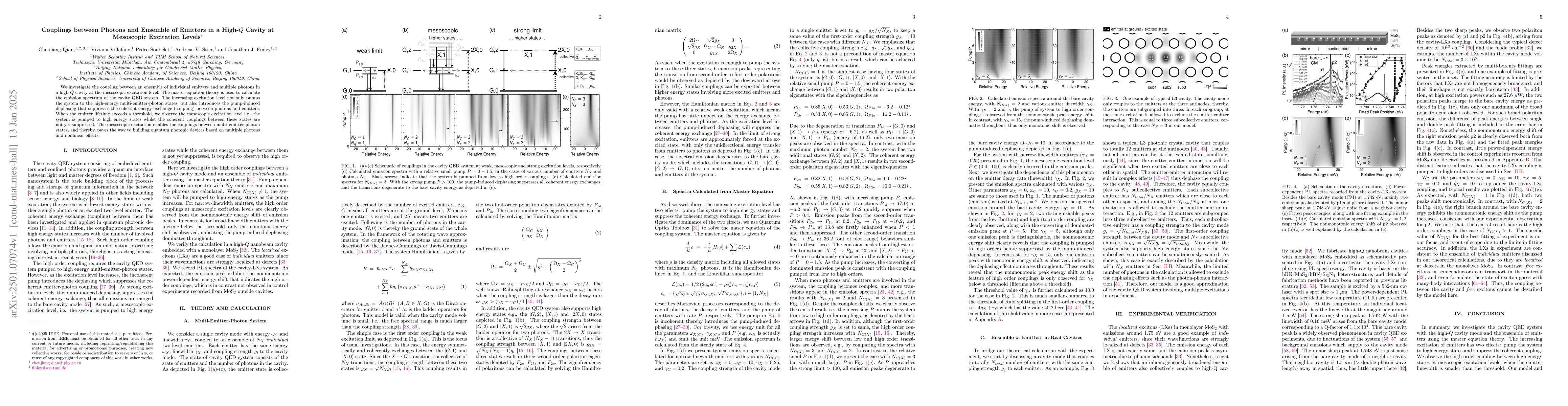
We investigate the coupling between an ensemble of individual emitters and multiple photons in a high-$Q$ cavity at the mesoscopic excitation level. The master equation theory is used to calculate the...
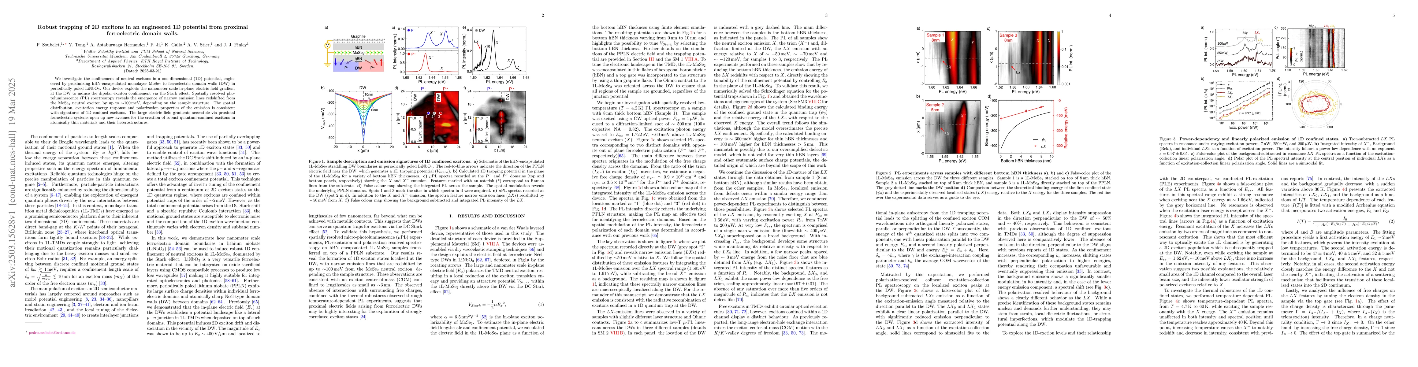
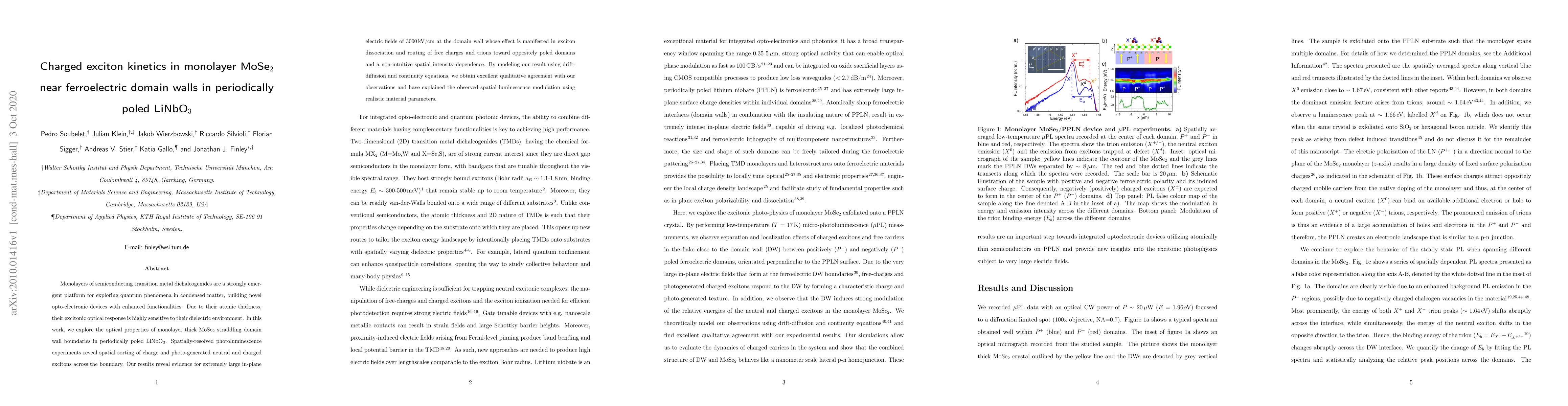
We investigate the confinement of neutral excitons in a one-dimensional (1D) potential, engineered by proximizing hBN-encapsulated monolayer MoSe$_2$ to ferroelectric domain walls (DW) in periodically...
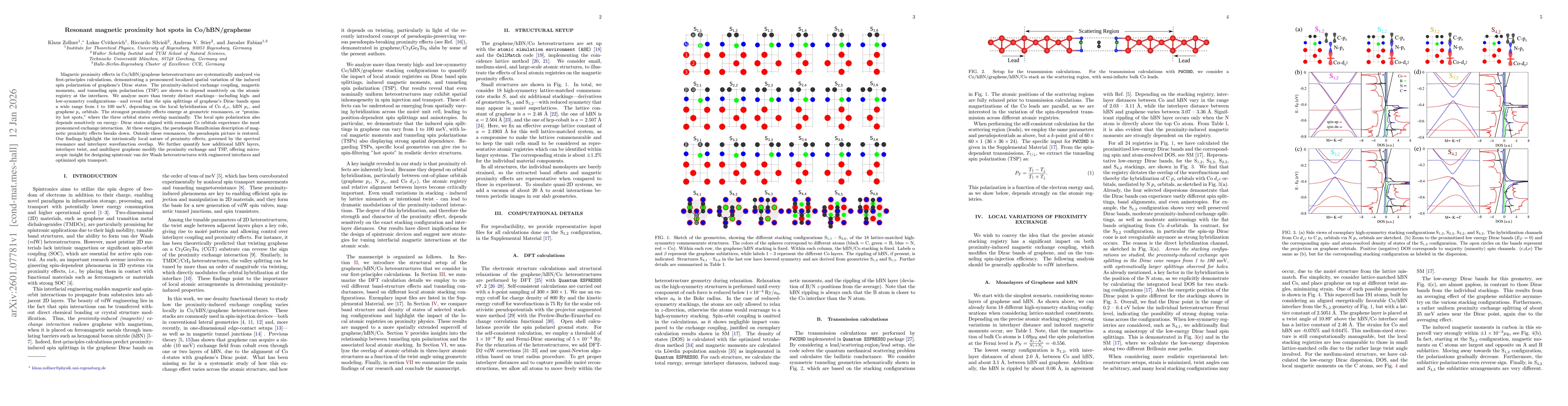
Magnetic proximity effects in Co/hBN/graphene heterostructures are systematically analyzed via first-principles calculations, demonstrating a pronounced localized spatial variation of the induced spin...
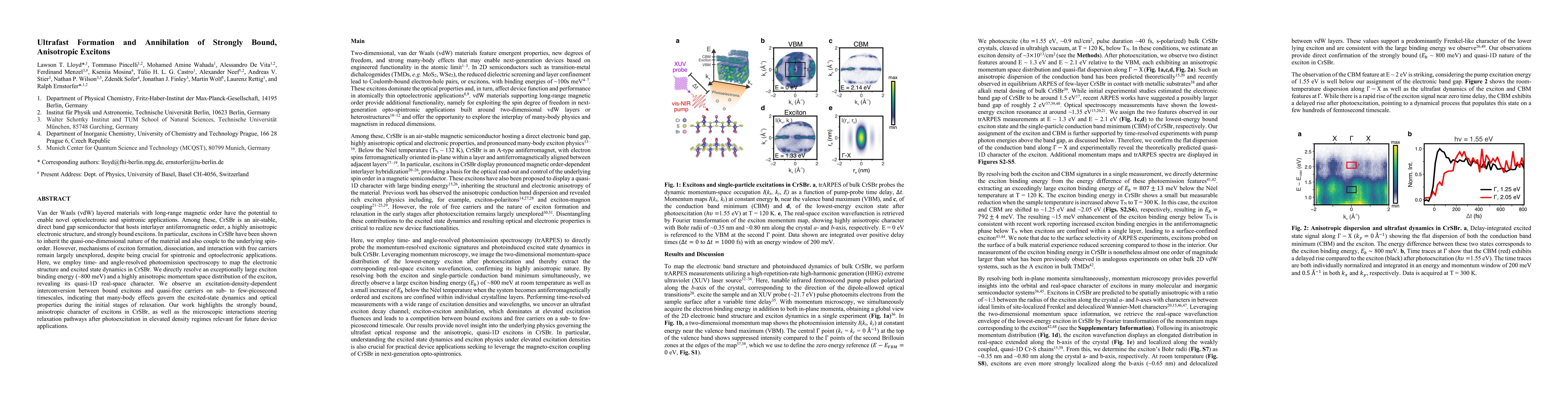
Van der Waals (vdW) layered materials with long-range magnetic order have the potential to enable novel optoelectronic and spintronic applications. Among these, CrSBr is an air-stable, direct band gap...