Academic Profile
Statistics
Similar Authors
Papers on arXiv
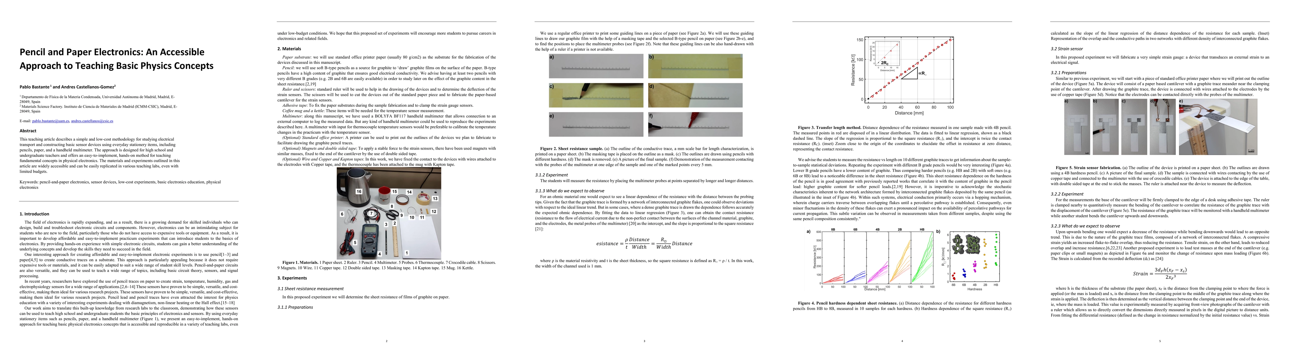
This teaching article describes a simple and low-cost methodology for studying electrical transport and constructing basic sensor devices using everyday stationery items, including pencils, paper, a...
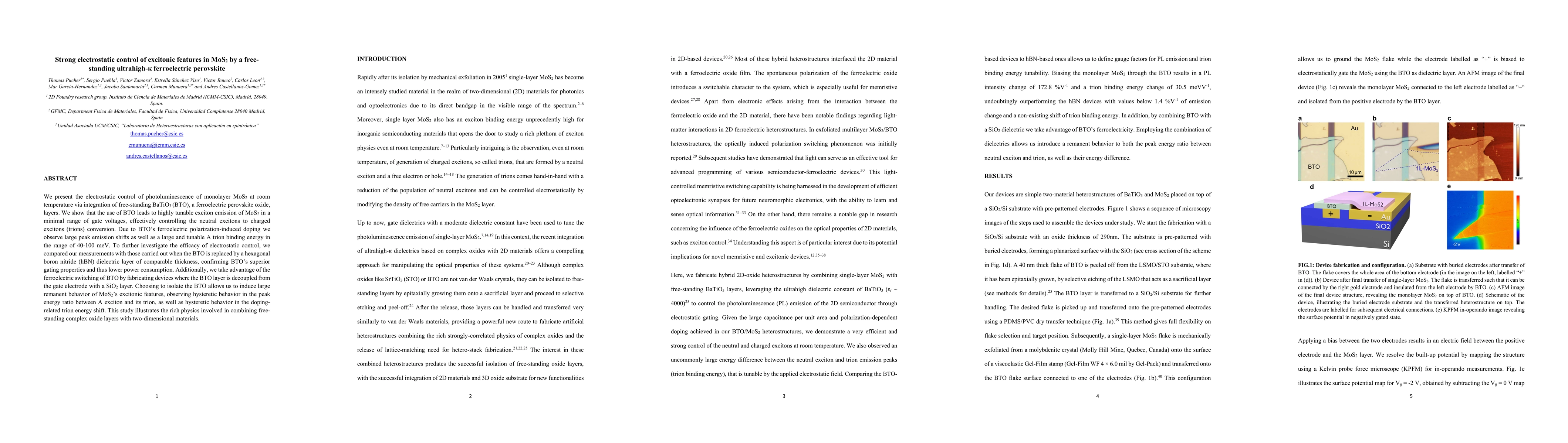
We present the electrostatic control of photoluminescence of monolayer MoS$_2$ at room temperature via integration of free-standing BaTiO$_3$ (BTO), a ferroelectric perovskite oxide, layers. We show...
Two-dimensional (2D) materials are widely used in various applications due to their extraordinary properties. In particular, their electrochemical stability, low electrical resistance, and huge spec...
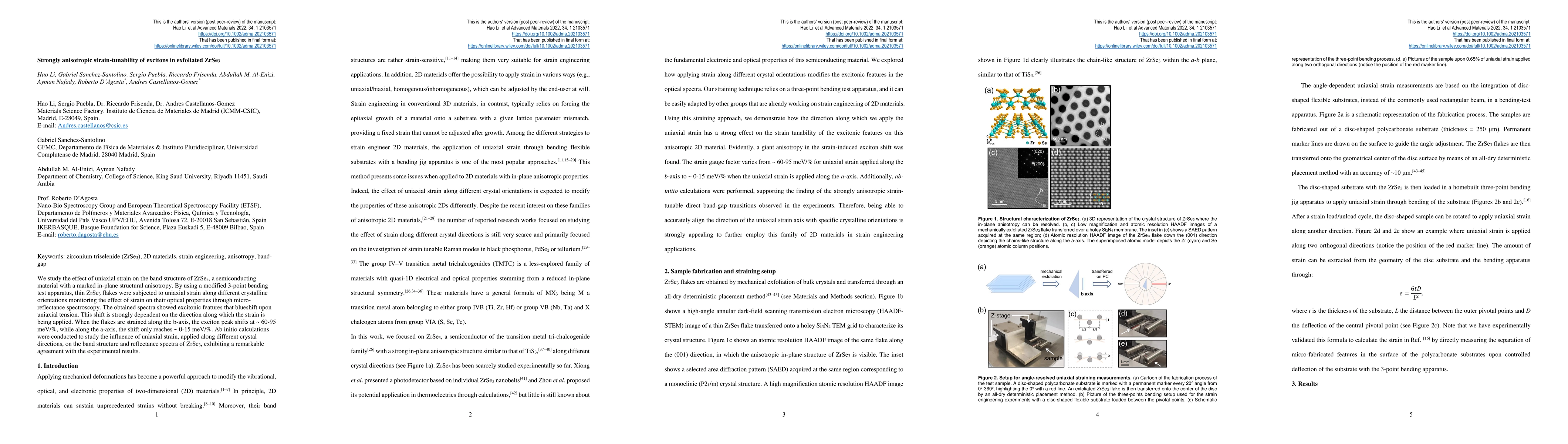
We study the effect of uniaxial strain on the band structure of ZrSe$_3$, a semiconducting material with a marked in-plane structural anisotropy. By using a modified 3-point bending test apparatus, ...
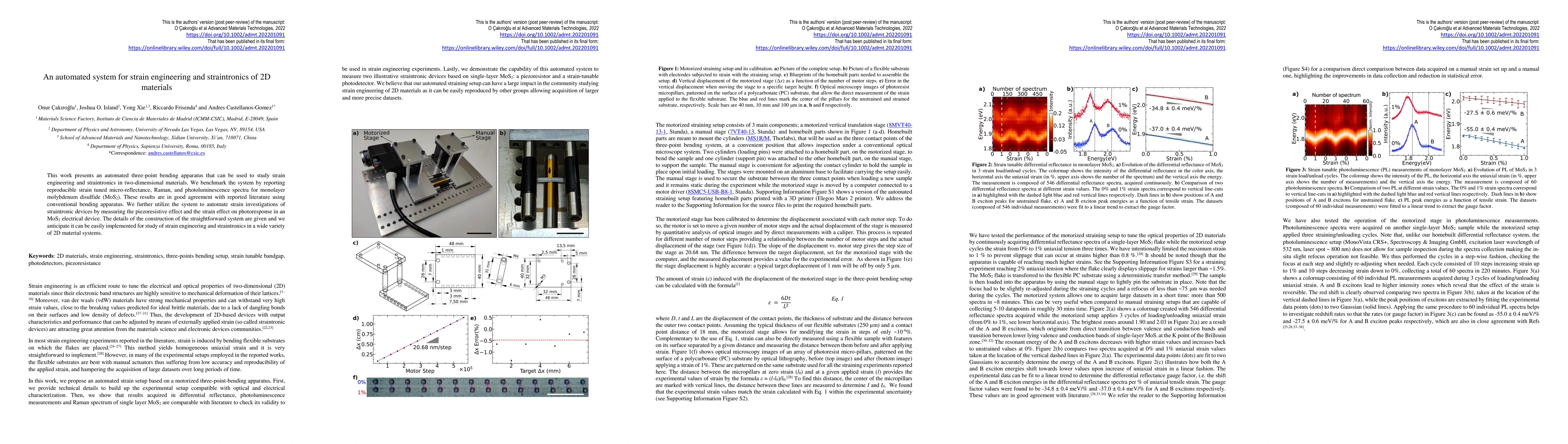
This work presents an automated three-point bending apparatus that can be used to study strain engineering and straintronics in two-dimensional materials. We benchmark the system by reporting reprod...
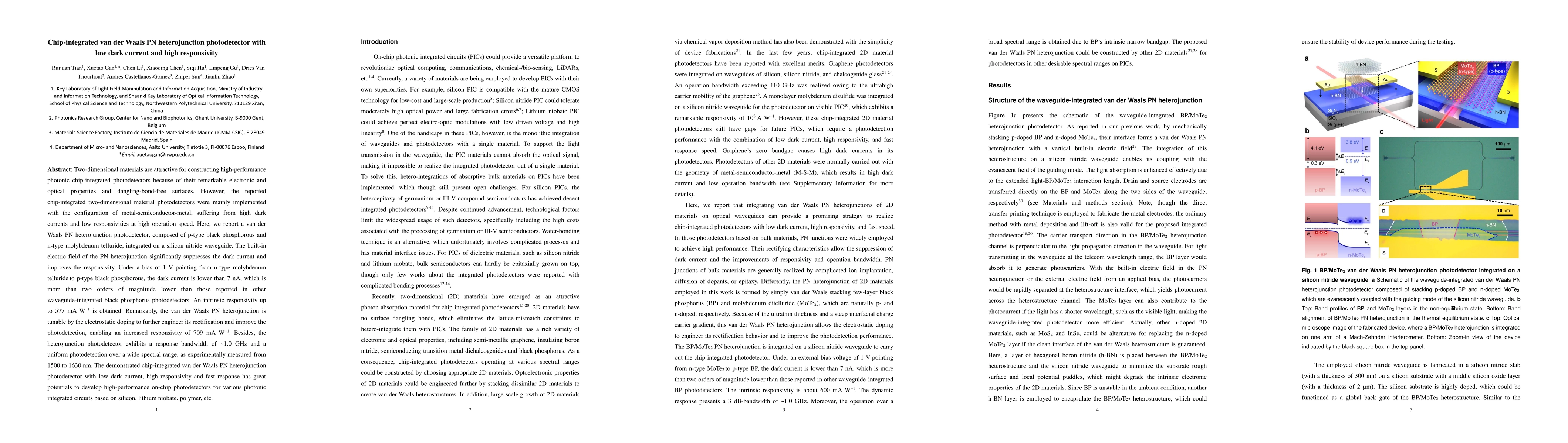
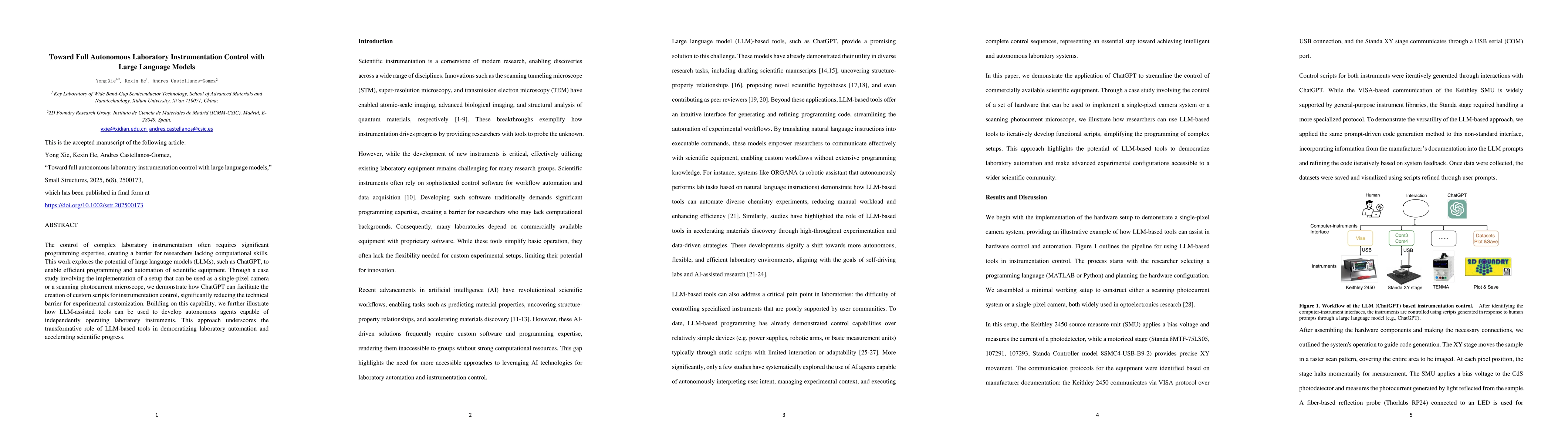
Two-dimensional materials are attractive for constructing high-performance photonic chip-integrated photodetectors because of their remarkable electronic and optical properties and dangling-bond-fre...
Paper offers a low-cost and widely available substrate for electronics. It posses alternative characteristics to silicon, as it shows low density and high-flexibility, together with biodegradability...
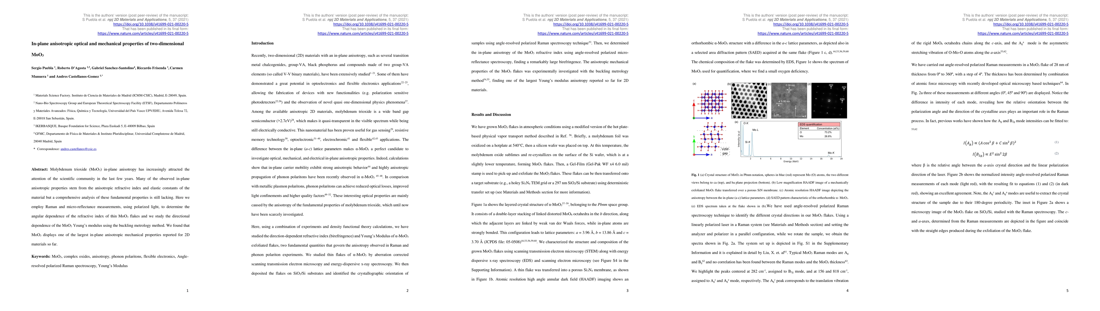
Molybdenum trioxide (MoO$_3$) in-plane anisotropy has increasingly attracted the attention of the scientific community in the last few years. Many of the observed in-plane anisotropic properties ste...
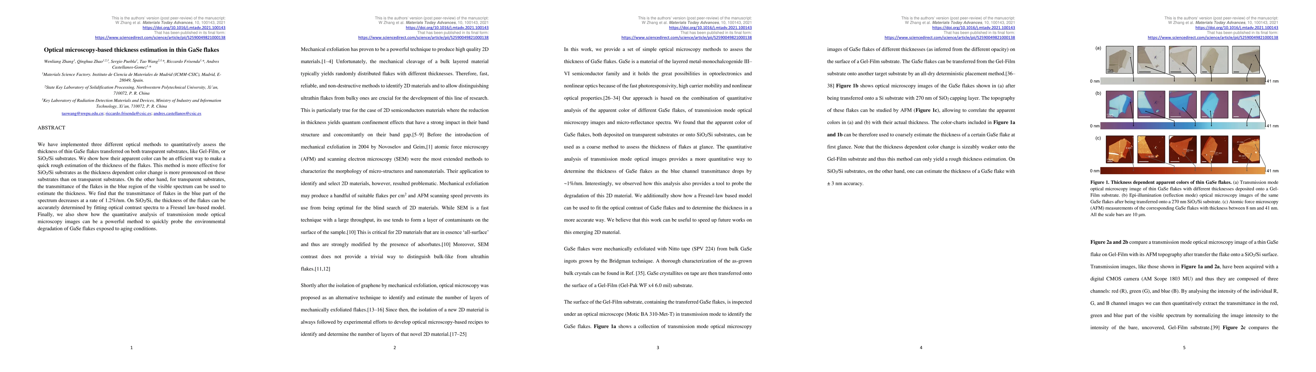
We have implemented three different optical methods to quantitatively assess the thickness of thin GaSe flakes transferred on both transparent substrates, like Gel-Film, or SiO2/Si substrates. We sh...
Paper has the potential to dramatically reduce the cost of electronic components. In fact, paper is 10 000 times cheaper than crystalline silicon, motivating the research to integrate electronic mat...
Paper holds the promise to replace silicon substrates in applications like internet of things or disposable electronics that require ultra-low-cost electronic components and an environmentally frien...
Strain engineering has arisen as a powerful technique to tune the electronic and optical properties of two-dimensional semiconductors like molybdenum disulfide (MoS2). Although several theoretical w...
Two-dimensional layered trichalcogenide materials have recently attracted the attention of the scientific community because of its robust mechanical, thermal properties and applications in opto and ...
Symmetry breaking in two-dimensional layered materials plays a significant role in their macroscopic electrical, optical, magnetic and topological properties, including but not limited to spin-polar...
Paper based thermoresistive sensors are fabricated by rubbing WS2 powder against a piece of standard copier paper, like the way a pencil is used to write on paper. The abrasion between the layered m...
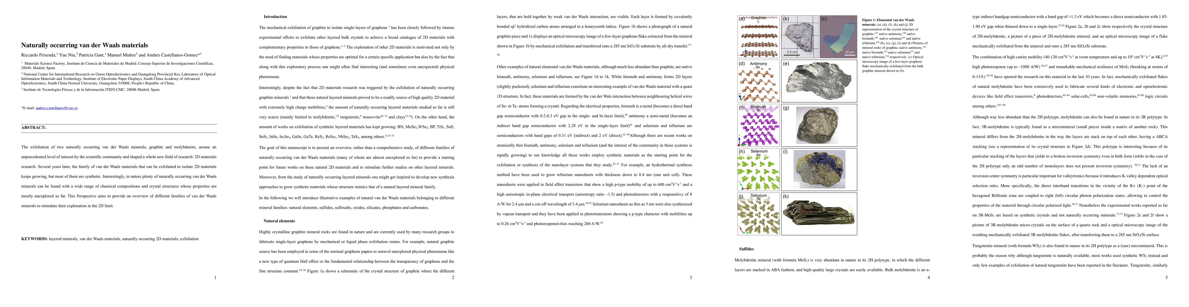
The exfoliation of two naturally occurring van der Waals minerals, graphite and molybdenite, arouse an unprecedented level of interest by the scientific community and shaped a whole new field of res...
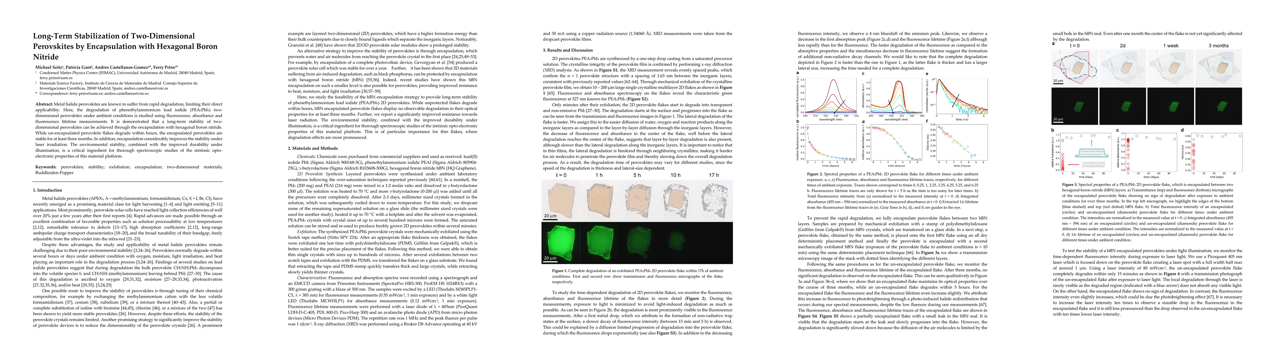
Metal halide perovskites are known to suffer from rapid degradation, limiting their direct applicability. Here, the degradation of phenethylammonium lead iodide (PEA2PbI4) two-dimensional perovskite...
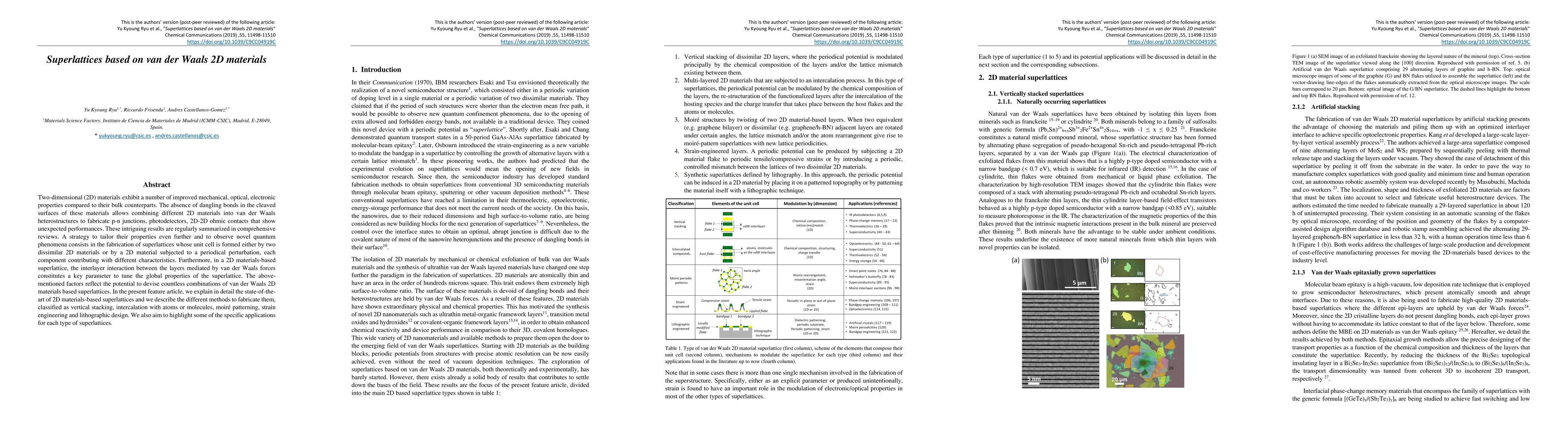
Two-dimensional (2D) materials exhibit a number of improved mechanical, optical, electronic properties compared to their bulk counterparts. The absence of dangling bonds in the cleaved surfaces of t...
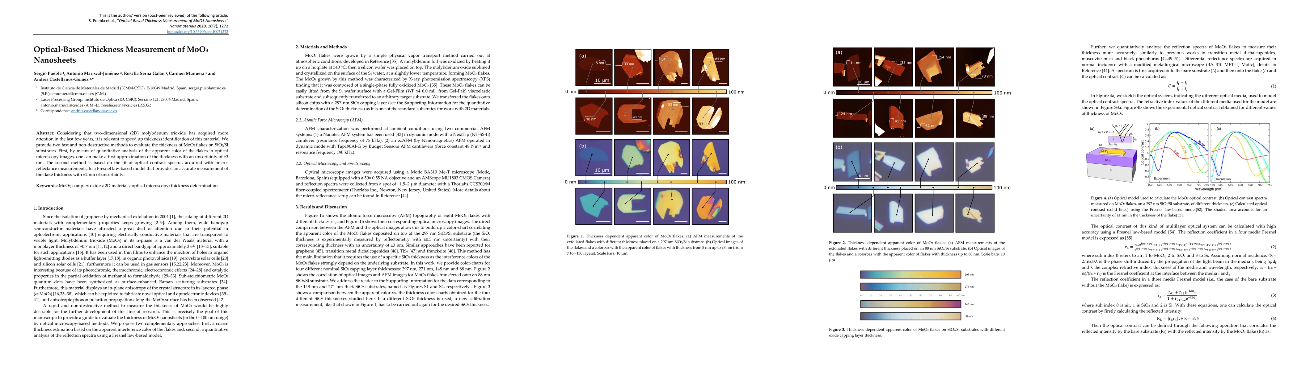
Considering that two-dimensional (2D) molybdenum trioxide has acquired more attention in the last few years, it is relevant to speed up thickness identification of this material. We provide two fast...
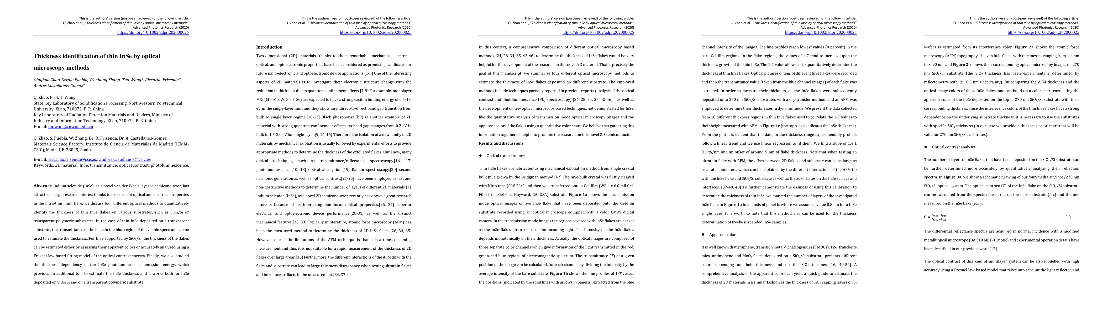
Indium selenide (InSe), as a novel van der Waals layered semiconductor, has attracted a large research interest thanks to its excellent optical and electrical properties in the ultra-thin limit. Her...
The ultrathin nature and dangling bonds free surface of two-dimensional (2D) semiconductors allow for significant modifications of their band gap through strain engineering. Here, thin InSe photodet...
Two-dimensional semiconductors are excellent candidates for next-generation electronics and optoelec-tronics thanks to their electrical properties and strong light-matter interaction. To fabricate d...
Due to the excellent electrical transport properties and optoelectronic performance, thin indium selenide (InSe) has recently attracted attention in the field of 2D semiconducting materials. However...
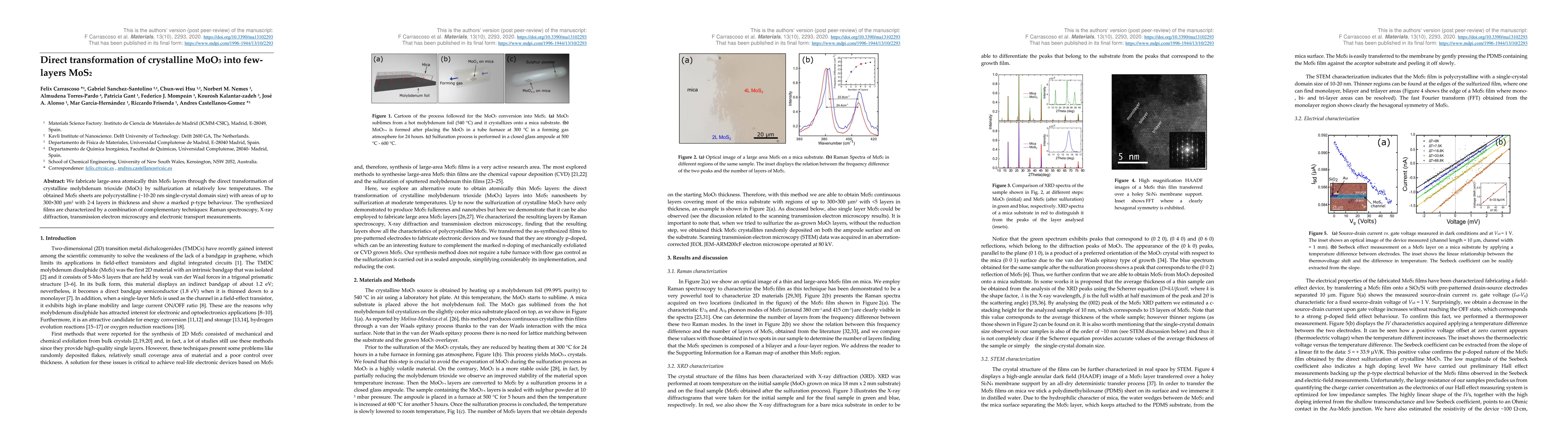
We fabricate large-area atomically thin MoS$_2$ layers through the direct transformation of crystalline molybdenum MoS$_2$ (MoO$_3$) by sulfurization at relatively low temperatures. The obtained MoS...
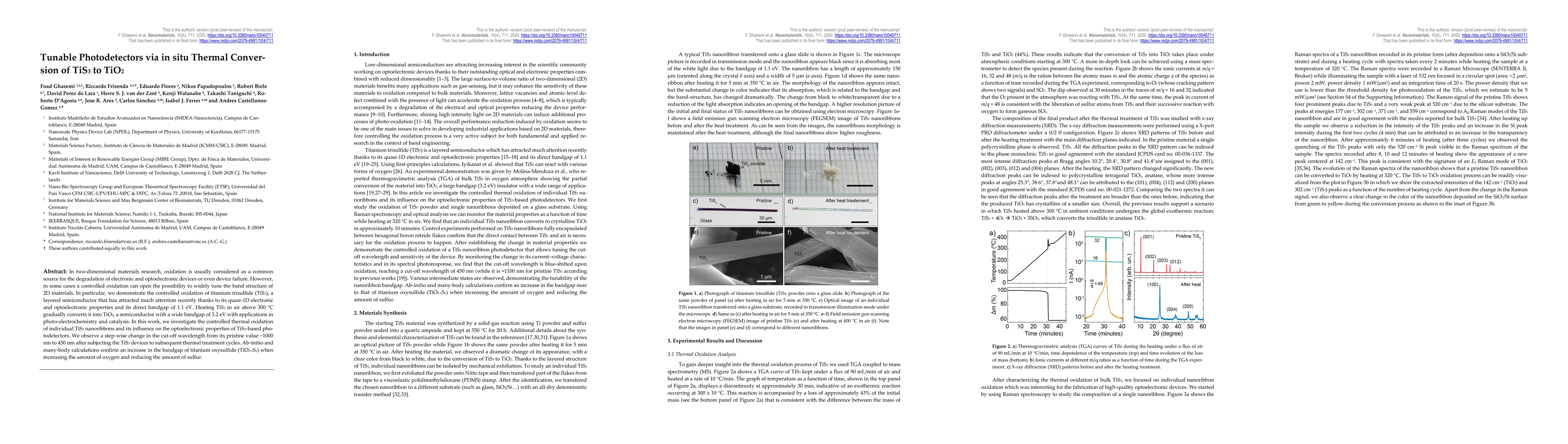
In two-dimensional materials research, oxidation is usually considered as a common source for the degradation of electronic and optoelectronic devices or even device failure. However, in some cases ...
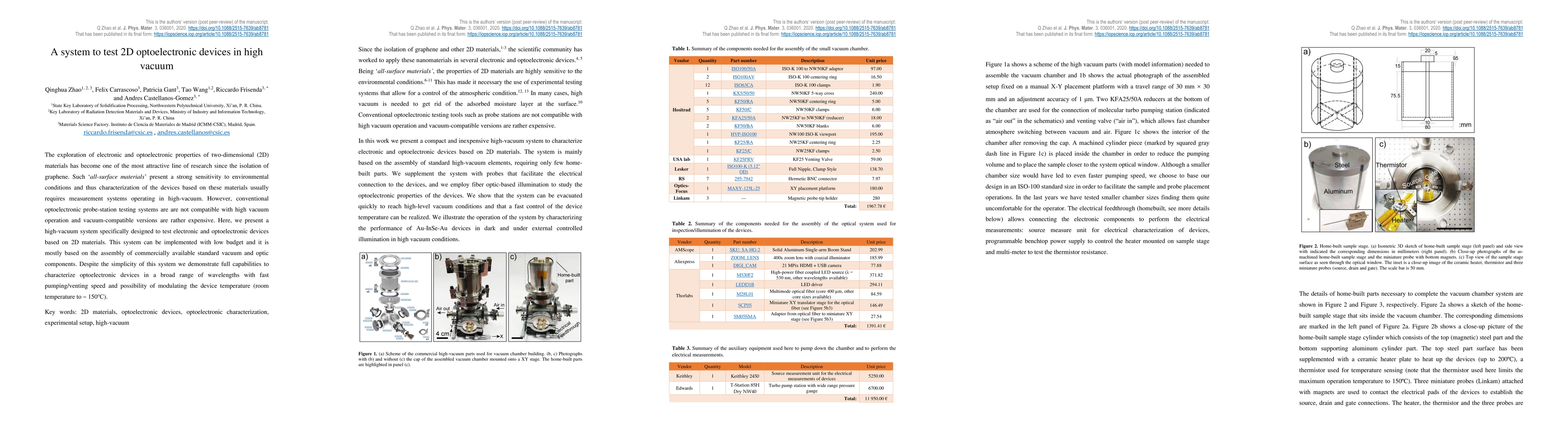
The exploration of electronic and optoelectronic properties of two-dimensional (2D) materials has become one of the most attractive line of research since the isolation of graphene. Such 'all-surfac...
Strain is a powerful tool to modify the optical properties of semiconducting transition metal dichalcogenides like MoS2, MoSe2, WS2 and WSe2. In this work we provide a thorough description of the te...
We present microfabricated thermal actuators to engineer the biaxial strain in two-dimensional (2D) materials. These actuators are based on microheater circuits patterned onto the surface of a polym...
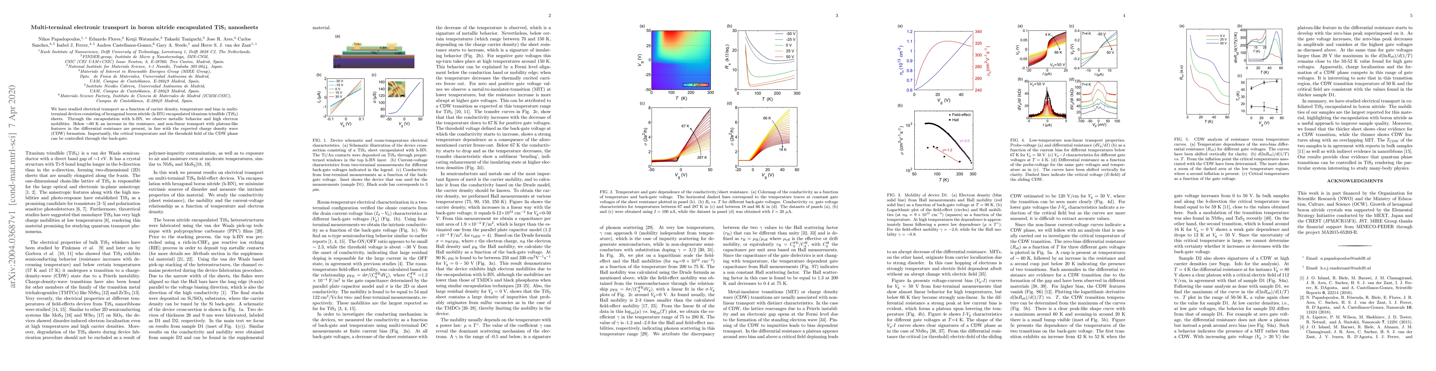
We have studied electrical transport as a function of carrier density, temperature and bias in multi-terminal devices consisting of hexagonal boron nitride (h-BN) encapsulated titanium trisulfide (T...
The isolation of air-sensitive two-dimensional (2D) materials and the race to achieve a better control of the interfaces in van der Waals heterostructures has pushed the scientific community towards...
Two-dimensional Indium Selenide (InSe) has attracted extensive attention recently due to its record-high charge carrier mobility and photoresponsivity in the fields of electronics and optoelectronic...
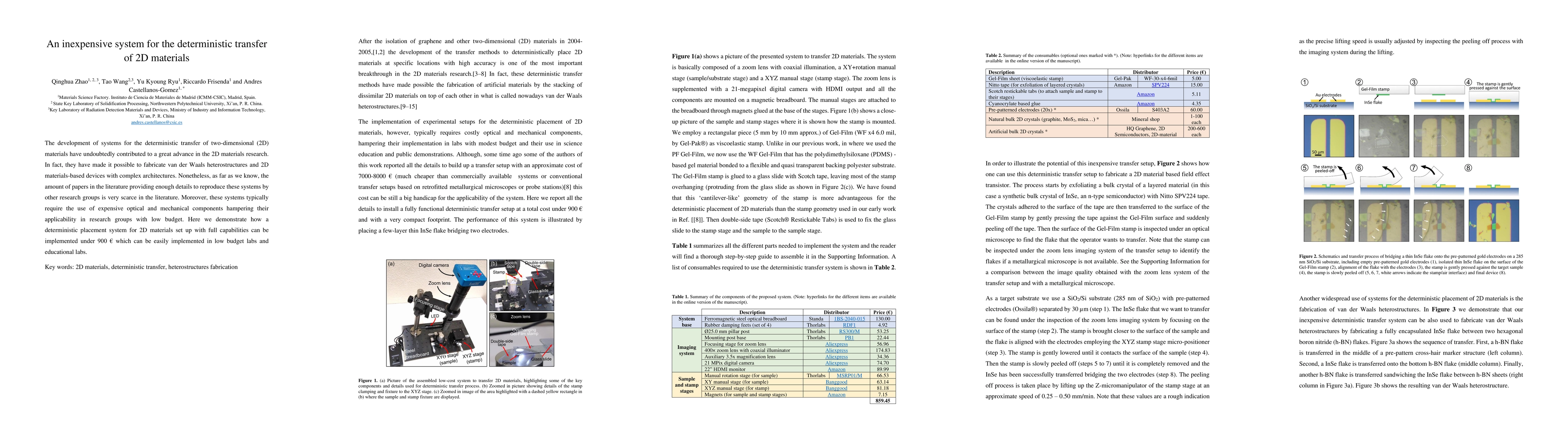
The development of systems for the deterministic transfer of two-dimensional (2D) materials have undoubtedly contributed to a great advance in the 2D materials research. In fact, they have made it p...
The successful application of titanium oxide-graphene hybrids in the fields of photocatalysis, photovoltaics and photodetection strongly depends on the interfacial contact between both materials. Th...
We show how the excitonic features of biaxial MoS2 flakes are very sensitive to biaxial strain. We find a lower bound for the gauge factors of the A exciton and B exciton of (-41 +- 2) meV/% and (-4...
When a two-dimensional material, adhered onto a compliant substrate, is subjected to compression it can undertake a buckling instability yielding to a periodic rippling. Interestingly, when black ph...
Here, we propose a method to determine the thickness of the most common transition metal dichalcogenides (TMDCs) placed on the surface of transparent stamps, used for the deterministic placement of ...
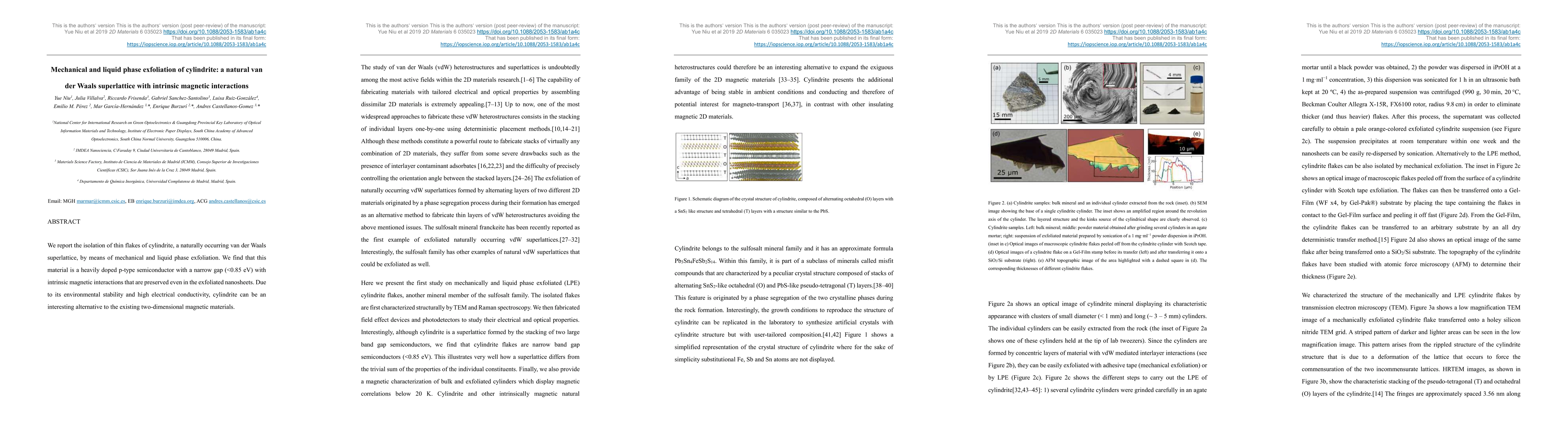
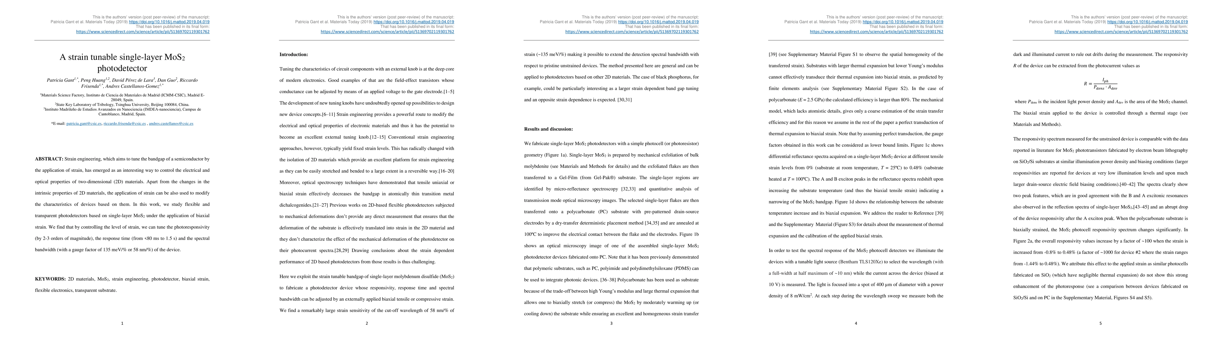
We report the isolation of thin flakes of cylindrite, a naturally occurring van der Waals superlattice, by means of mechanical and liquid phase exfoliation. We find that this material is a heavily d...
Strain engineering, which aims to tune the bandgap of a semiconductor by the application of strain, has emerged as an interesting way to control the electrical and optical properties of two-dimensio...
TiS3 nanosheets have proven to be promising candidates for ultrathin optoelectronic devices due to their direct narrow band-gap and the strong light-matter interaction. In addition, the marked in-pl...
Stacking monolayers of transition metal dichalcogenides (TMDs) has led to the discovery of a plethora of new exotic phenomena, resulting from moir\'e pattern formation. Due to the atomic thickness and...
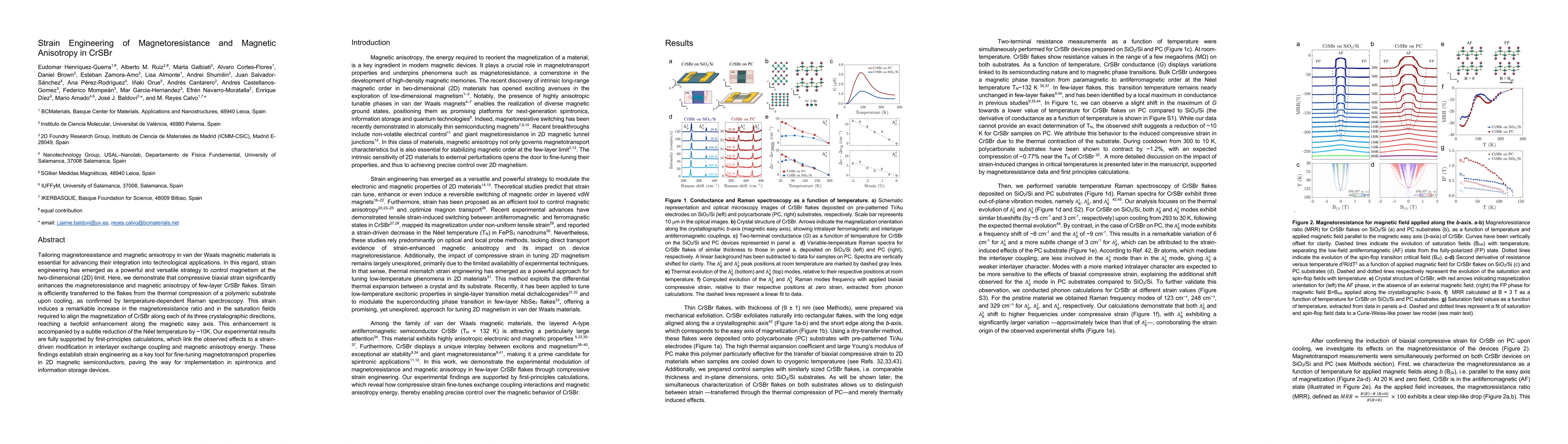
Tailoring magnetoresistance and magnetic anisotropy in van der Waals magnetic materials is essential for advancing their integration into technological applications. In this regard, strain engineering...
The integration of high-dielectric-constant (high-$\kappa$) materials with two-dimensional (2D) semiconductors is promising to overcome performance limitations and reach their full theoretical potenti...
We present a scalable method for direct patterning of graphite and transition metal dichalcogenide (TMD) films on polycarbonate (PC) and other transparent substrates using fiber laser ablation. This p...
We systematically investigate the influence of polyvinyl formal (PVFM), commonly known as Formvar, in comparison to polycarbonate (PC) and polymethyl methacrylate (PMMA), as encapsulation materials on...
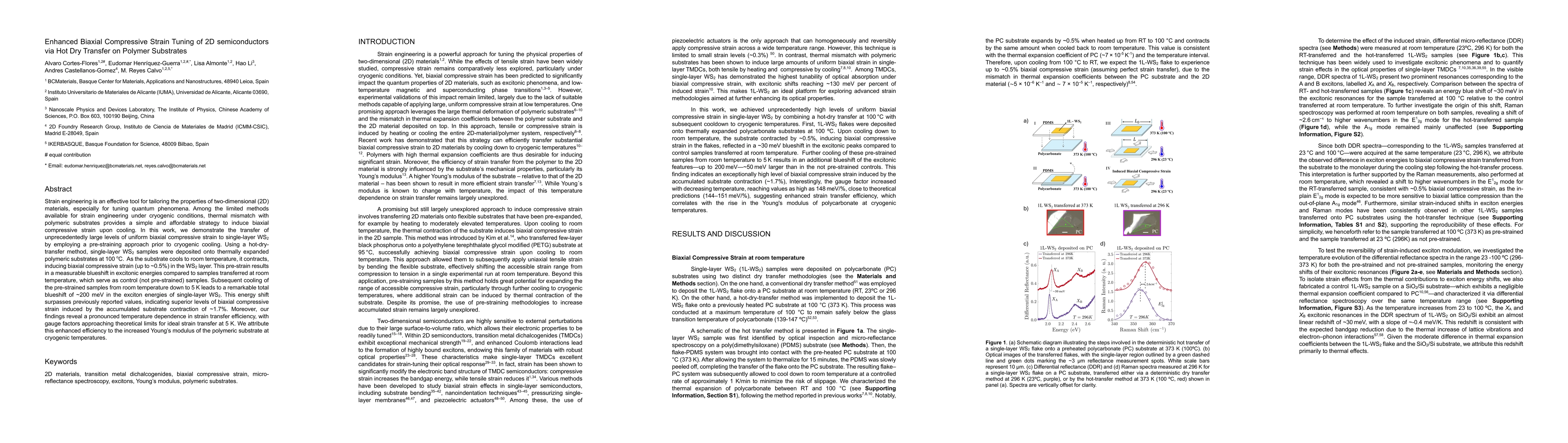
Strain engineering is an effective tool for tailoring the properties of two-dimensional (2D) materials, especially for tuning quantum phenomena. Among the limited methods available for strain engineer...
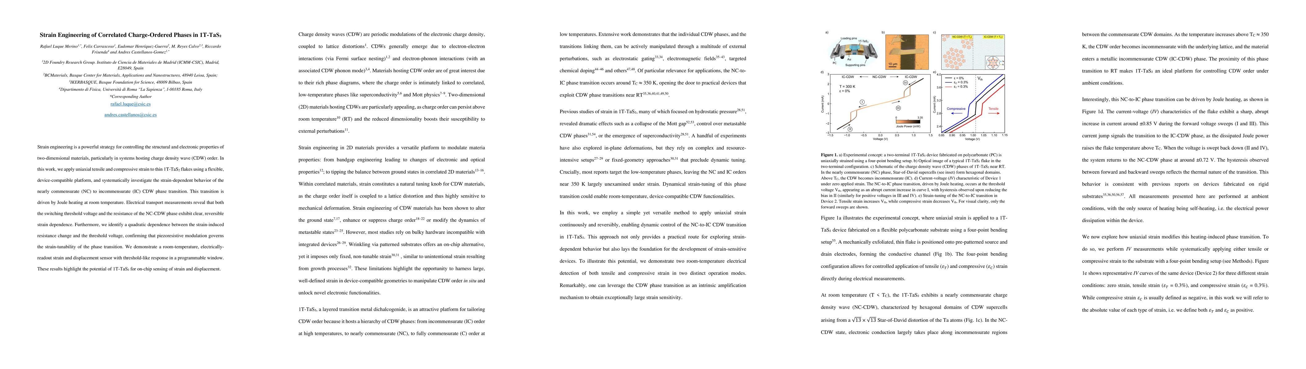
Strain engineering is a powerful strategy for controlling the structural and electronic properties of two-dimensional materials, particularly in systems hosting charge density wave (CDW) order. In thi...
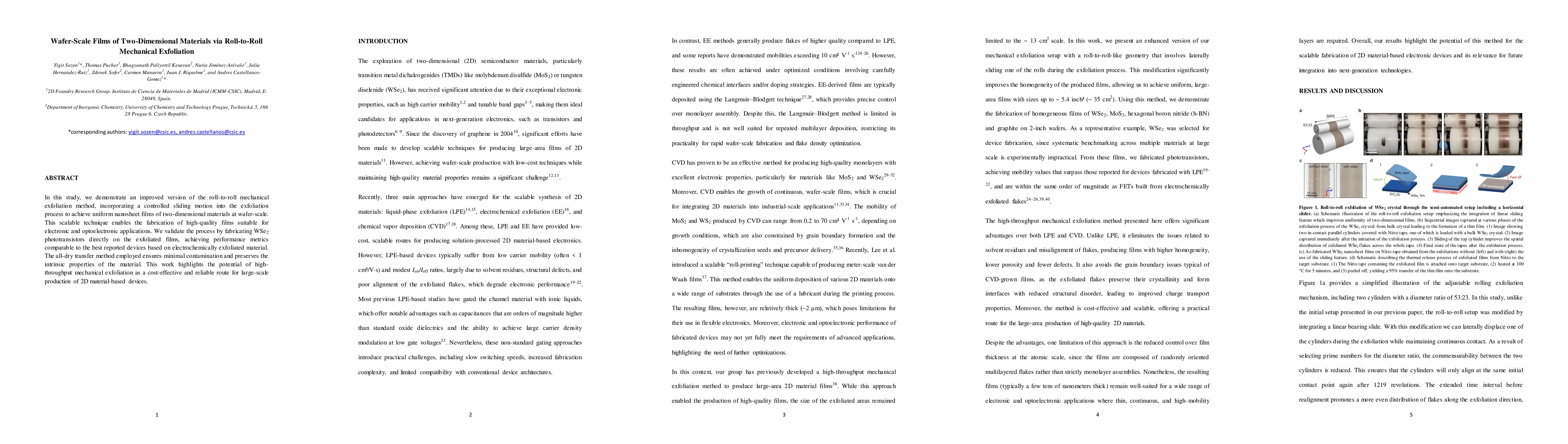
In this study, we demonstrate an improved version of the roll-to-roll mechanical exfoliation method, incorporating a controlled sliding motion into the exfoliation process to achieve uniform nanosheet...
Tunable superconductors provide a versatile platform for advancing next-generation quantum technologies. Here, we demonstrate controllable superconductivity in suspended NbSe2 thin layers, achieved th...
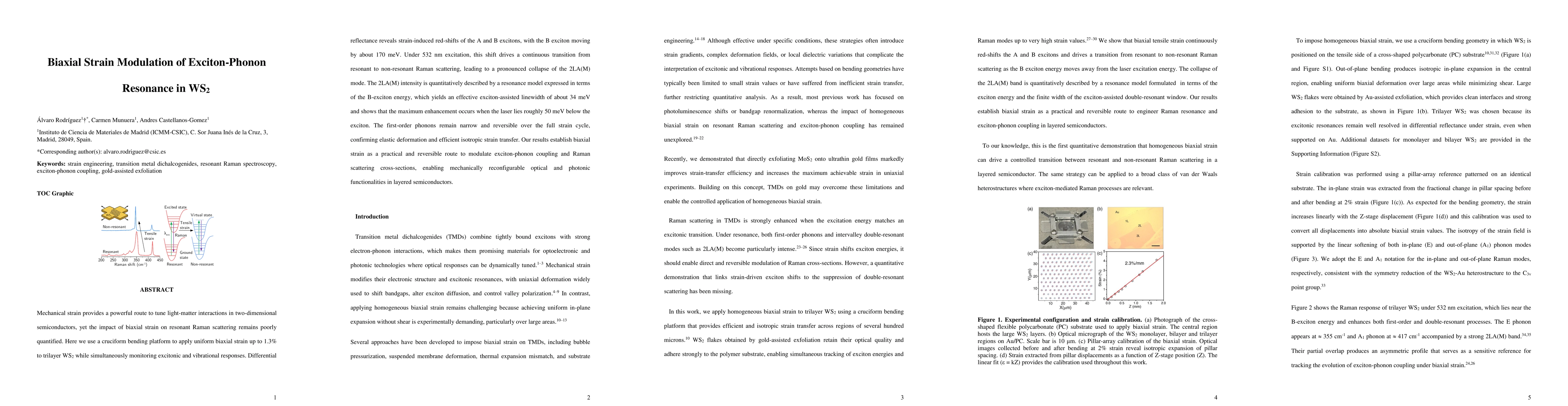
Mechanical strain provides a powerful route to tune light-matter interactions in two-dimensional semiconductors, yet the impact of biaxial strain on resonant Raman scattering remains poorly quantified...
The control of complex laboratory instrumentation often requires significant programming expertise, creating a barrier for researchers lacking computational skills. This work explores the potential of...