ArxivLens
A
Researcher

Anton Murros

5 papers on arXiv

5 arXiv Papers
9 Total Publications
Profile

Academic Profile

Name A. Murros
Total Papers 9
Scholar Profile View on Semantic Scholar
Metrics

Statistics

5 arXiv Papers
9 Total Publications
Publications

Papers on arXiv

Thumbnail for Terahertz detection with graphene FETs: photothermoelectric and
  resistive self-mixing contributions to the detector response
arXiv
Terahertz detection with graphene FETs: photothermoelectric and resistive self-mixing contributions to the detector response

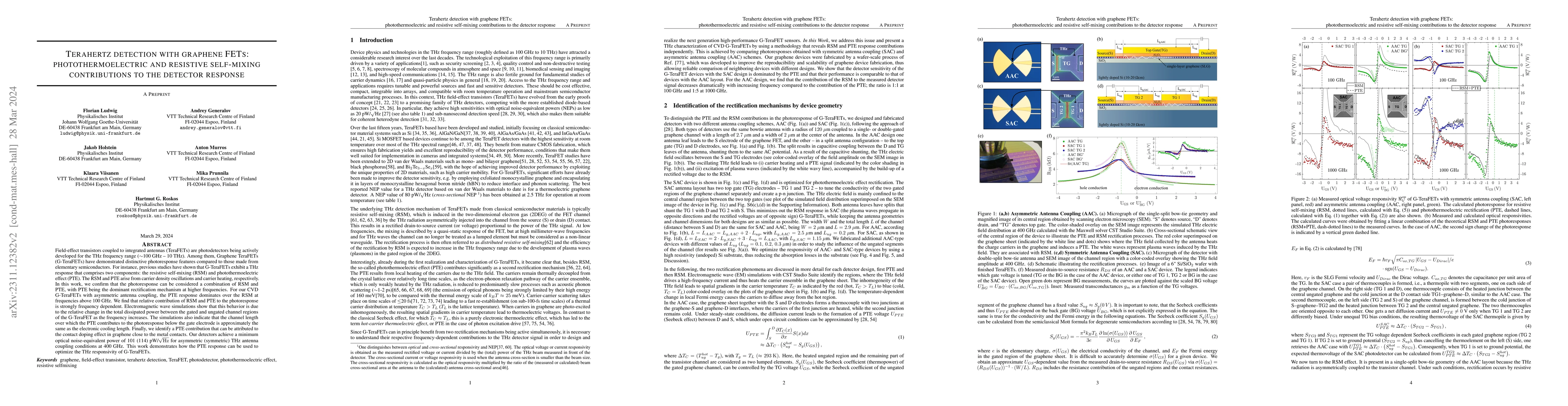
Field-effect transistors coupled to integrated antennas (TeraFETs) are photodetectors being actively developed for the THz frequency range ($\sim$ 100 GHz - 10 THz). Among them, Graphene TeraFETs (G...

Thumbnail for Wafer-scale graphene field-effect transistor biosensor arrays with
  monolithic CMOS readout
arXiv
Wafer-scale graphene field-effect transistor biosensor arrays with monolithic CMOS readout

The reliability of analysis is becoming increasingly important as point-of-care diagnostics are transitioning from single analyte detection towards multiplexed multianalyte detection. Multianalyte d...

Thumbnail for Geometrical magnetoresistance effect and mobility in graphene
  field-effect transistors
arXiv
Geometrical magnetoresistance effect and mobility in graphene field-effect transistors

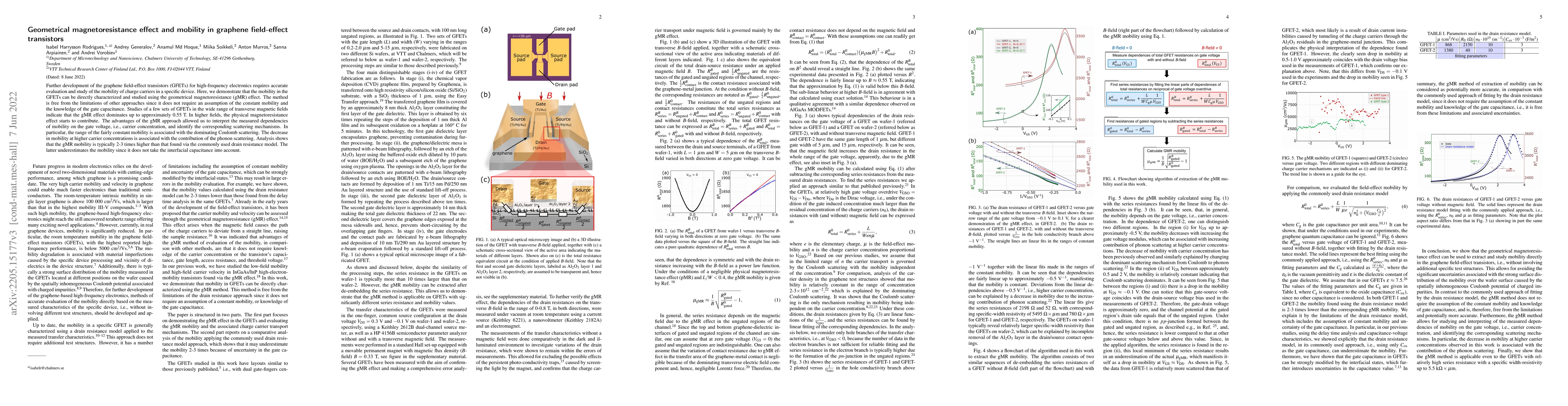
Further development of the graphene field-effect transistors (GFETs) for high-frequency electronics requires accurate evaluation and study of the mobility of charge carriers in a specific device. He...

Thumbnail for Infrared Bolometers Based on 40-nm-Thick Nano-Thermoelectric Silicon
  Membranes
arXiv
Infrared Bolometers Based on 40-nm-Thick Nano-Thermoelectric Silicon Membranes

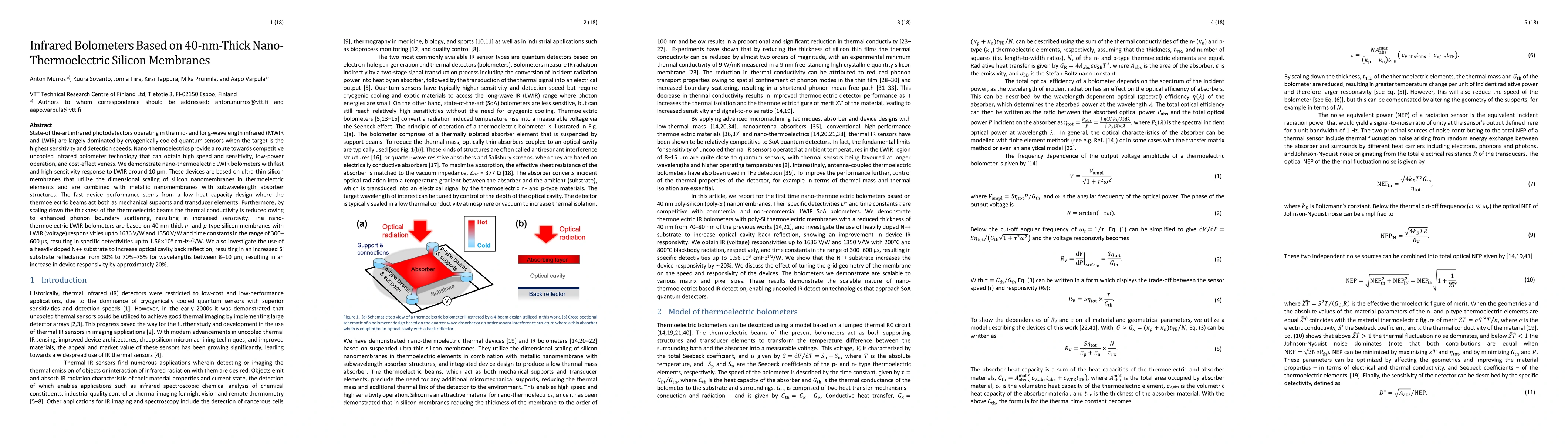
State-of the-art infrared photodetectors operating in the mid- and long-wavelength infrared (MWIR and LWIR) are largely dominated by cryogenically cooled quantum sensors when the target is the highest...

Thumbnail for Graphene FET Process and Analysis Optimization in 200 mm Pilot Line Environment
arXiv
Graphene FET Process and Analysis Optimization in 200 mm Pilot Line Environment

The maturity of the chemical vapor deposition graphene-based device processing has increased from chip level demonstrations to wafer-scale fabrication in the past few years. Due to this wafer-scale, e...

This website uses cookies to ensure you get the best experience. Learn more