Asir Intisar Khan
9 papers on arXiv
Academic Profile
Statistics
Similar Authors
Papers on arXiv
Non-volatile Phase-only Transmissive Spatial Light Modulators
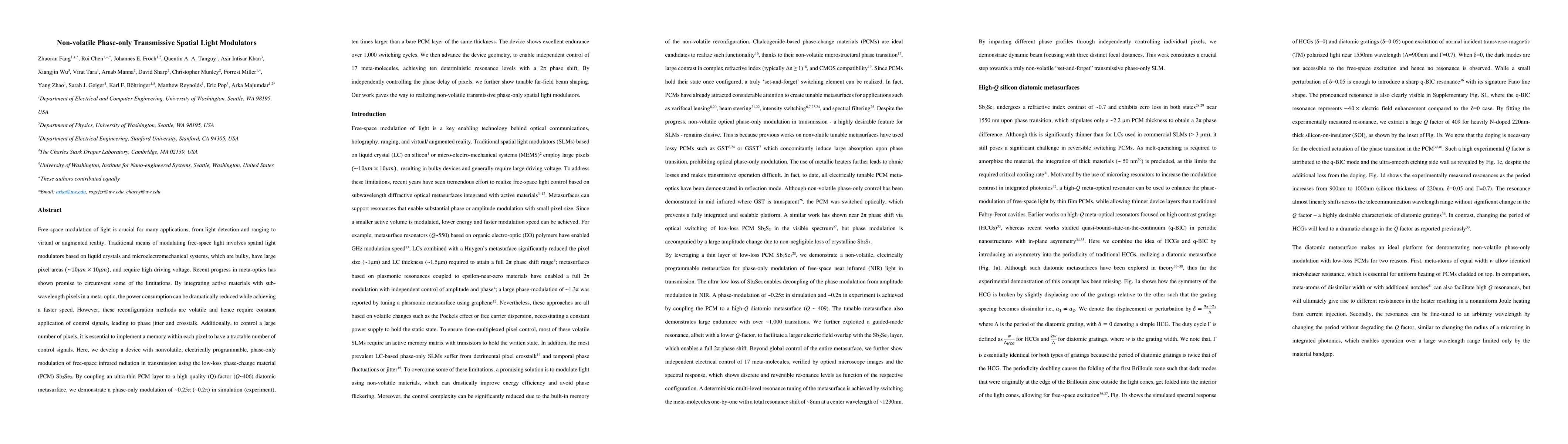
Free-space modulation of light is crucial for many applications, from light detection and ranging to virtual or augmented reality. Traditional means of modulating free-space light involves spatial l...
Improved Gradual Resistive Switching Range and 1000x On/Off Ratio in HfOx RRAM Achieved with a $Ge_2Sb_2Te_5$ Thermal Barrier
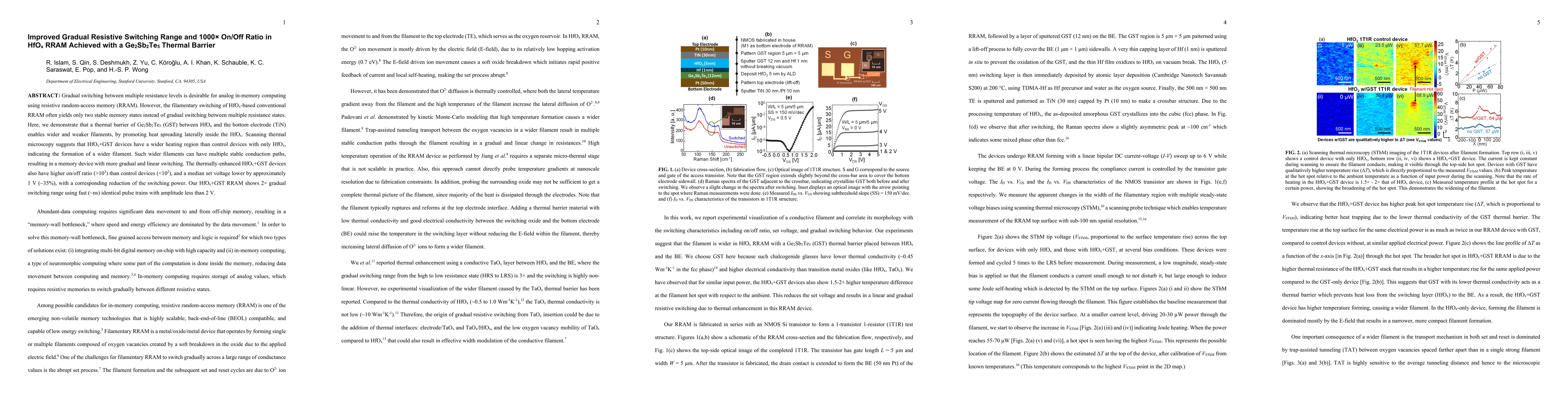
Gradual switching between multiple resistance levels is desirable for analog in-memory computing using resistive random-access memory (RRAM). However, the filamentary switching of $HfO_x$-based conv...
Enhanced Meta-Displays Using Advanced Phase-Change Materials
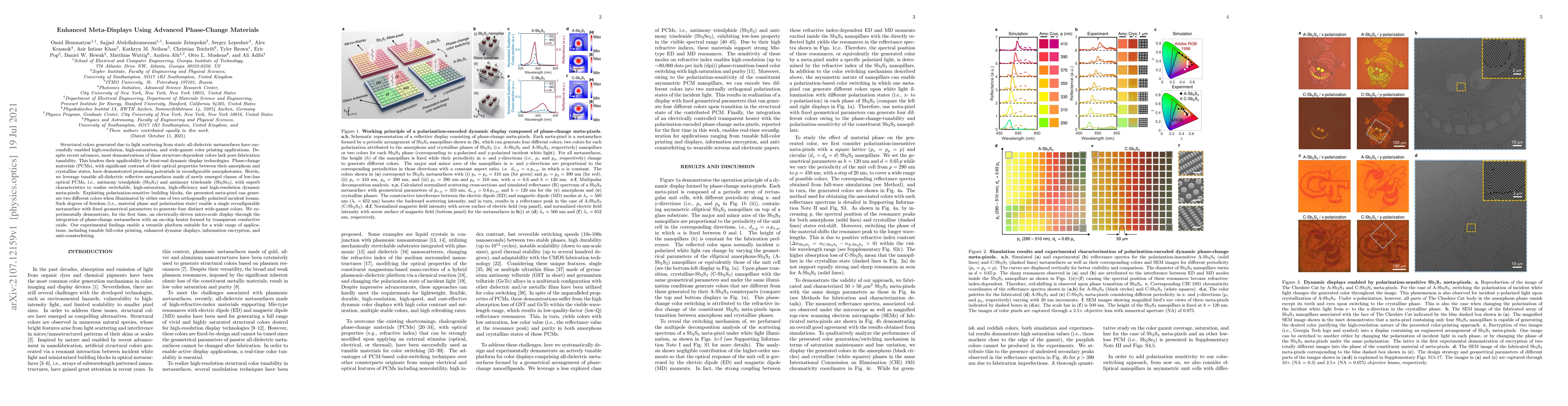
Structural colors generated due to light scattering from static all-dielectric metasurfaces have successfully enabled high-resolution, high-saturation, and wide-gamut color printing applications. De...
Lateral Transport and Field-Effect Characteristics of Sputtered P-Type Chalcogenide Thin Films
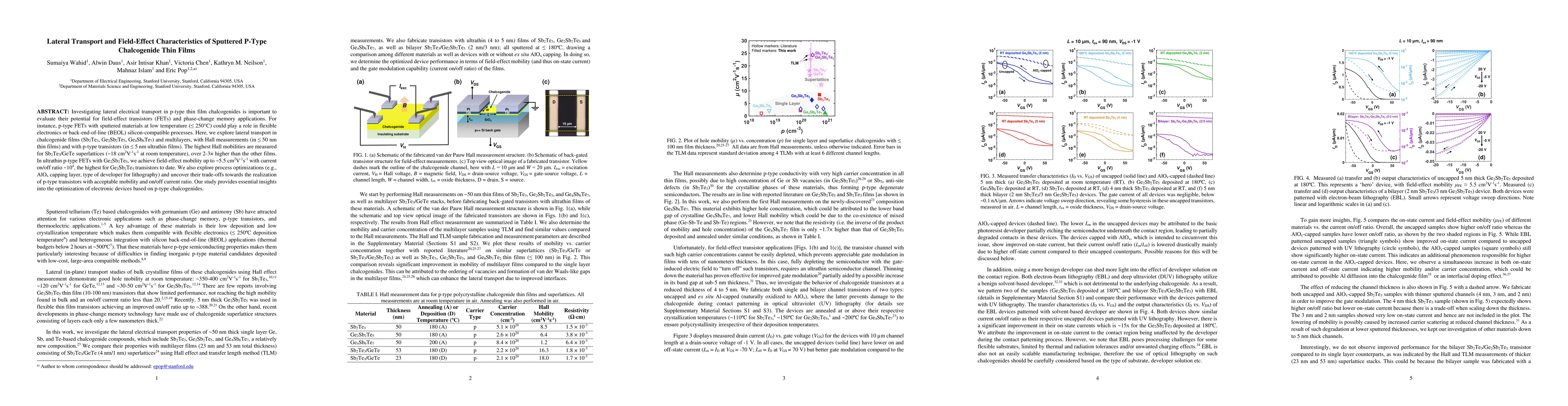
Investigating lateral electrical transport in p-type thin film chalcogenides is important to evaluate their potential for field-effect transistors (FETs) and phase-change memory applications. For in...
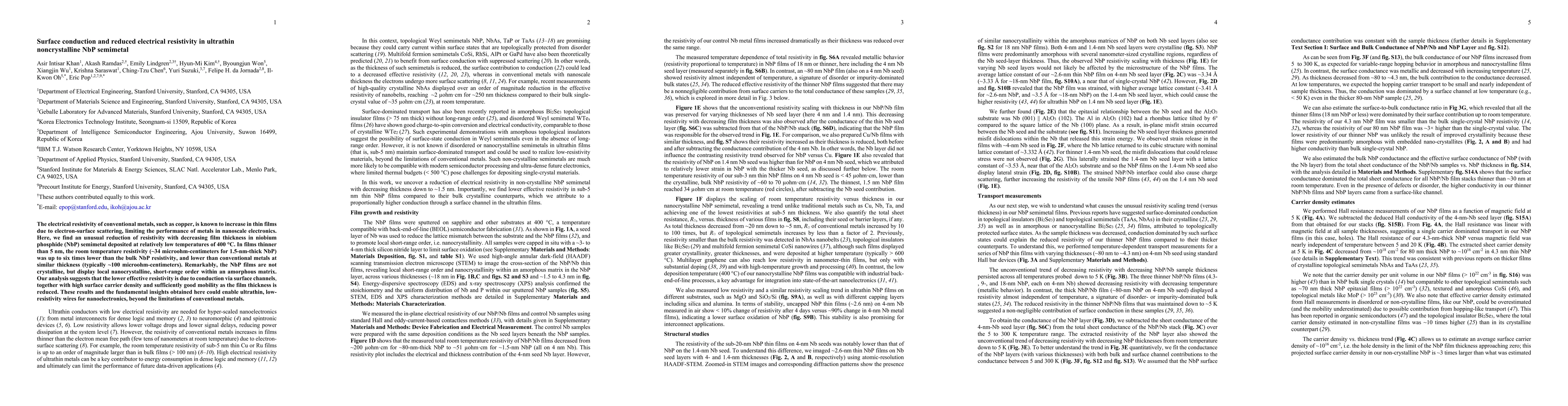
Surface Conduction and Reduced Electrical Resistivity in Ultrathin Non-Crystalline NbP Semimetal
The electrical resistivity of conventional metals, such as copper, is known to increase in thinner films due to electron-surface scattering, limiting the performance of metals in nanoscale electronics...
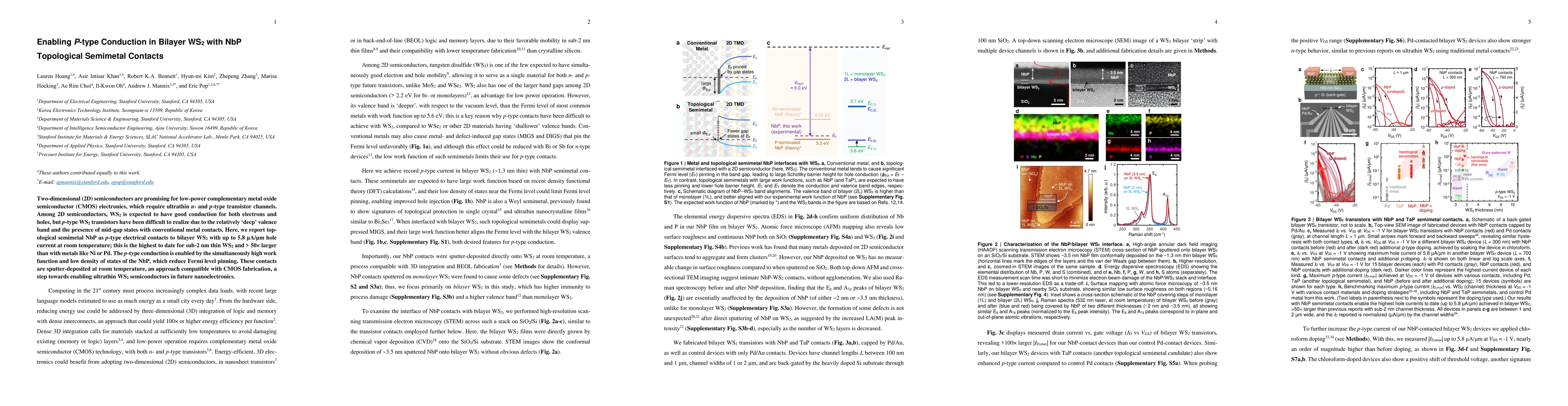
Enabling P-type Conduction in Bilayer WS2 with NbP Topological Semimetal Contacts
Two-dimensional (2D) semiconductors are promising for low-power complementary metal oxide semiconductor (CMOS) electronics, which require ultrathin n- and p-type transistor channels. Among 2D semicond...
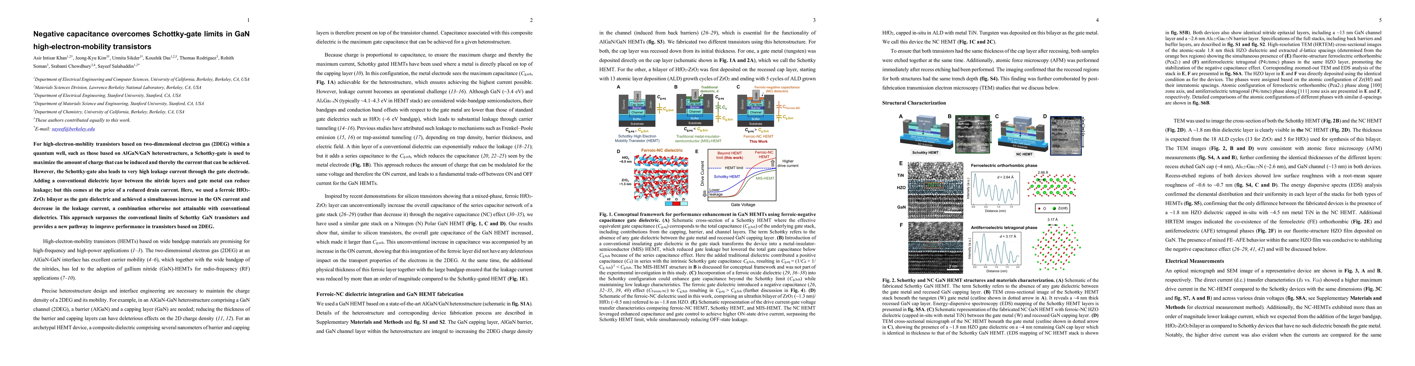
Negative capacitance overcomes Schottky-gate limits in GaN high-electron-mobility transistors
For high-electron-mobility transistors based on two-dimensional electron gas (2DEG) within a quantum well, such as those based on AlGaN/GaN heterostructure, a Schottky-gate is used to maximize the amo...
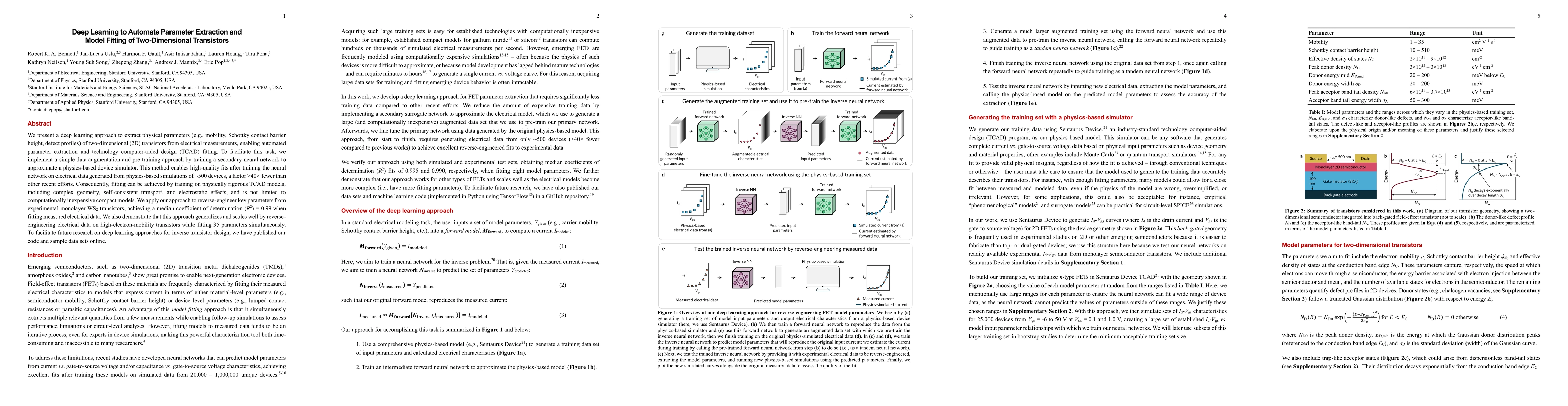
Deep Learning to Automate Parameter Extraction and Model Fitting of Two-Dimensional Transistors
We present a deep learning approach to extract physical parameters (e.g., mobility, Schottky contact barrier height, defect profiles) of two-dimensional (2D) transistors from electrical measurements, ...
Scale-robust Low Resistance Transport in Atomic Layer Deposited Topological Semimetal Wafers on Amorphous Substrate
As data-centric computing advances, energy-efficient interconnects are increasingly critical for AI-driven systems. Traditional metal conductors face severe limitations at nanoscale due to increased r...