Academic Profile
Statistics
Similar Authors
Papers on arXiv
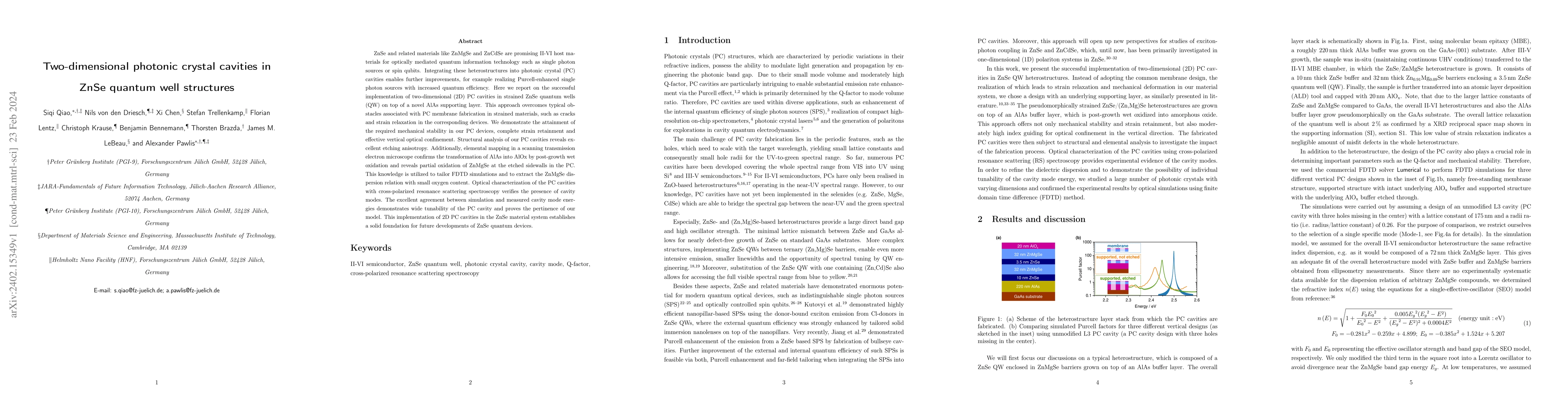
ZnSe and related materials like ZnMgSe and ZnCdSe are promising II-VI host materials for optically mediated quantum information technology such as single photon sources or spin qubits. Integrating t...
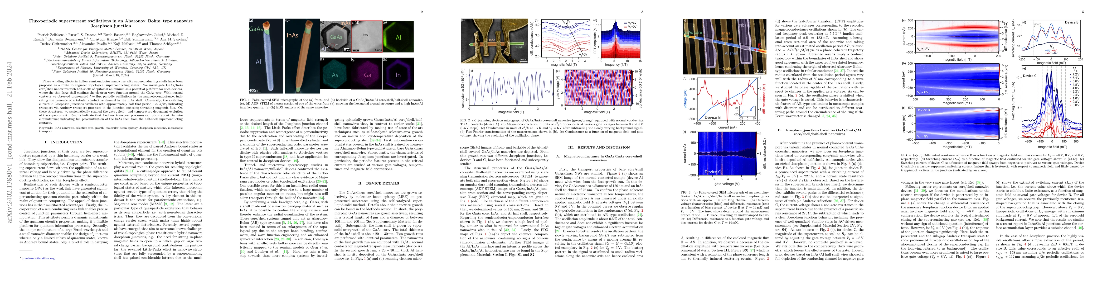
Phase winding effects in hollow semiconductor nanowires with superconducting shells have been proposed as a route to engineer topological superconducting states. We investigate GaAs/InAs core/shell ...
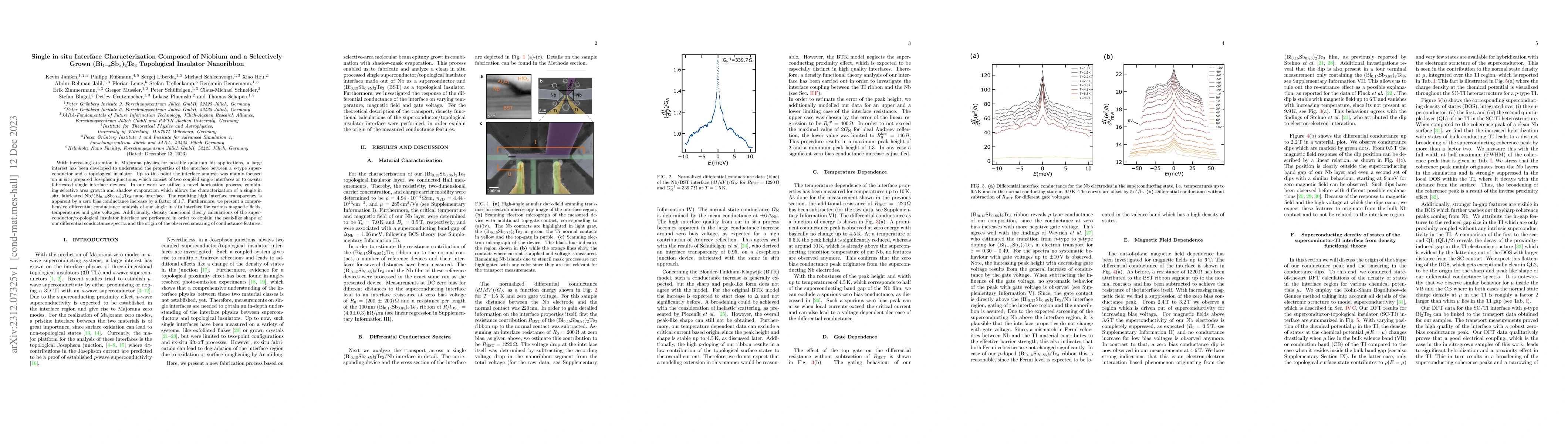
With increasing attention in Majorana physics for possible quantum bit applications, a large interest has been developed to understand the properties of the interface between a $s$-type superconduct...
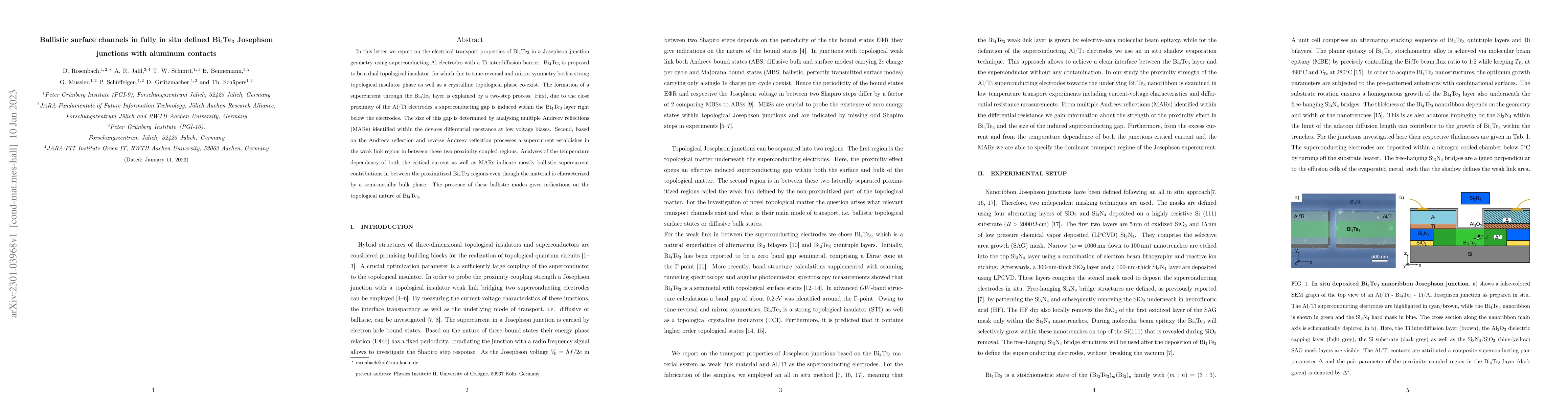
In this letter we report on the electrical transport properties of Bi$_4$Te$_3$ in a Josephson junction geometry using superconducting Al electrodes with a Ti interdiffusion barrier. Bi$_4$Te$_3$ is...
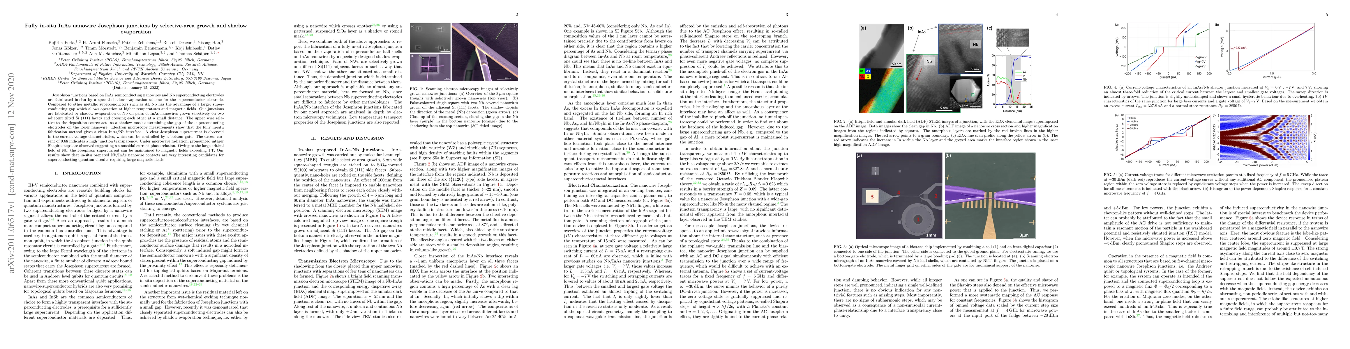
Josephson junctions based on InAs semiconducting nanowires and Nb superconducting electrodes are fabricated in-situ by a special shadow evaporation scheme for the superconductor electrode. Compared ...
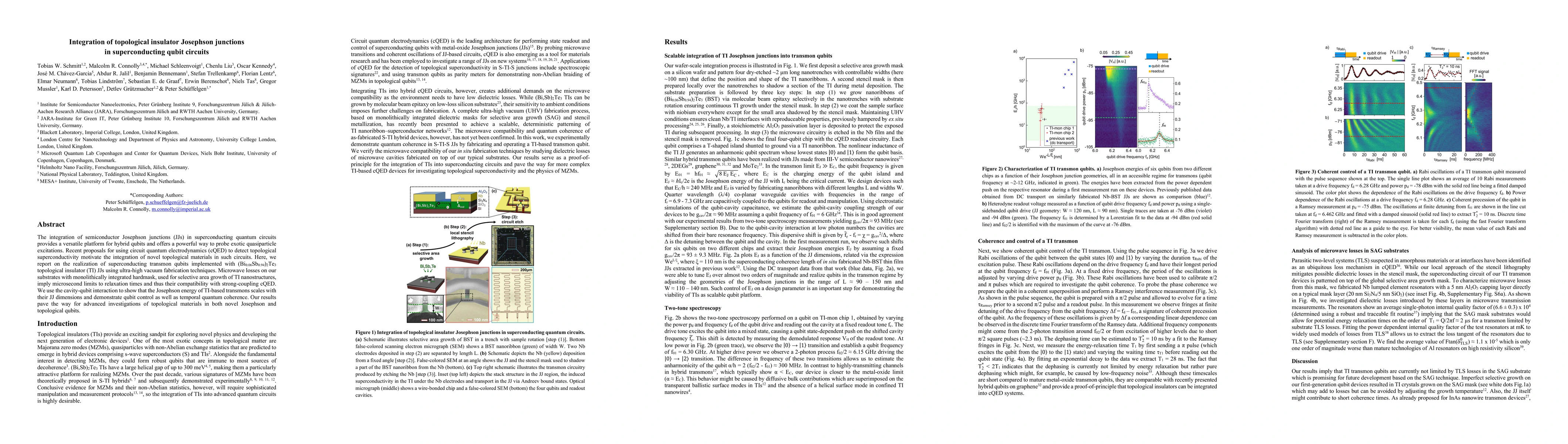
The integration of semiconductor Josephson junctions (JJs) in superconducting quantum circuits provides a versatile platform for hybrid qubits and offers a powerful way to probe exotic quasiparticle...
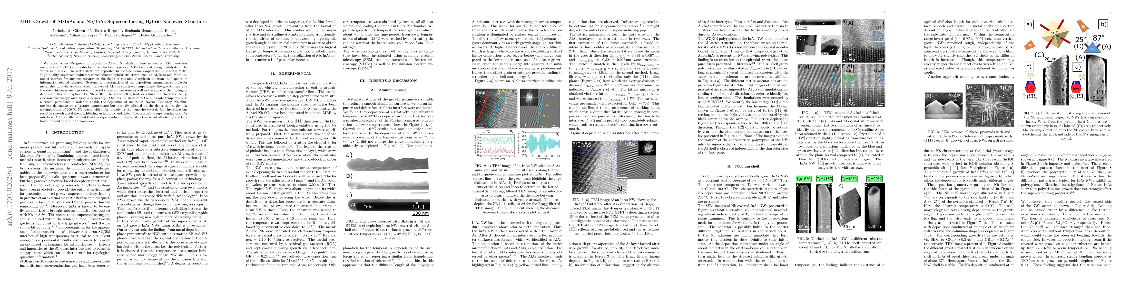
We report on \textit{in situ} growth of crystalline Al and Nb shells on InAs nanowires. The nanowires are grown on Si(111) substrates by molecular beam epitaxy (MBE) without foreign catalysts in the...
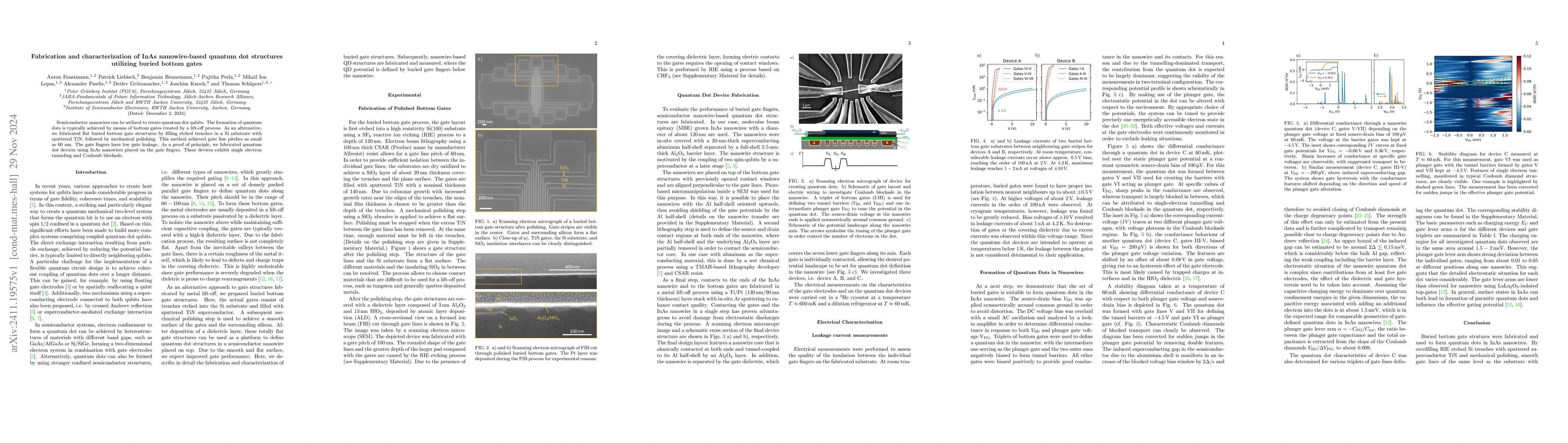
Semiconductor nanowires can be utilized to create quantum dot qubits. The formation of quantum dots is typically achieved by means of bottom gates created by a lift-off process. As an alternative, we ...
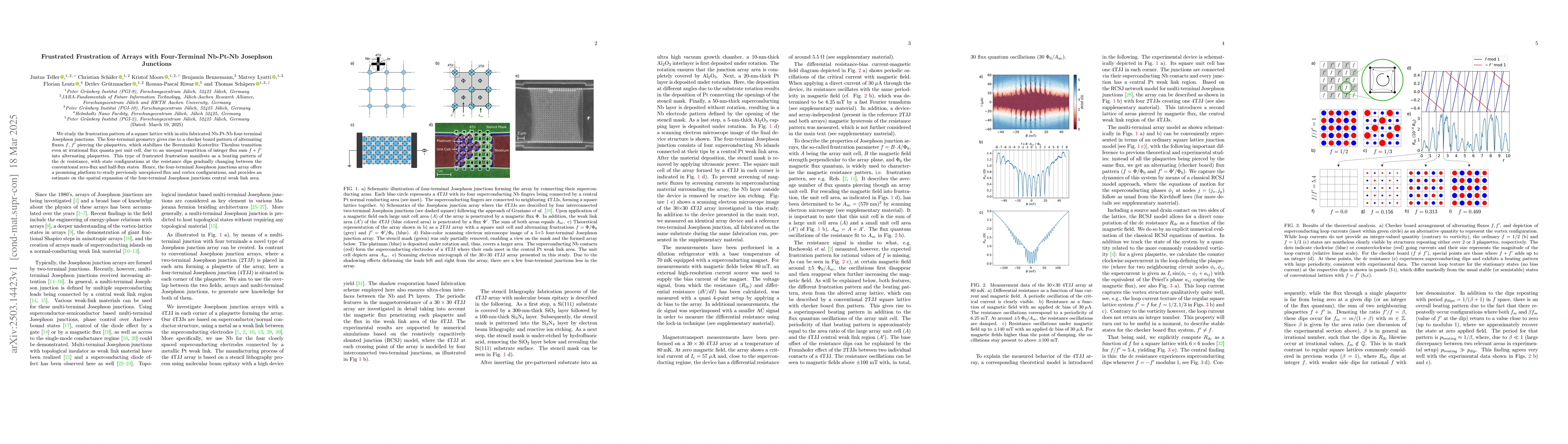
We study the frustration pattern of a square lattice with in-situ fabricated Nb-Pt-Nb four-terminal Josephson junctions. The four-terminal geometry gives rise to a checker board pattern of alternating...
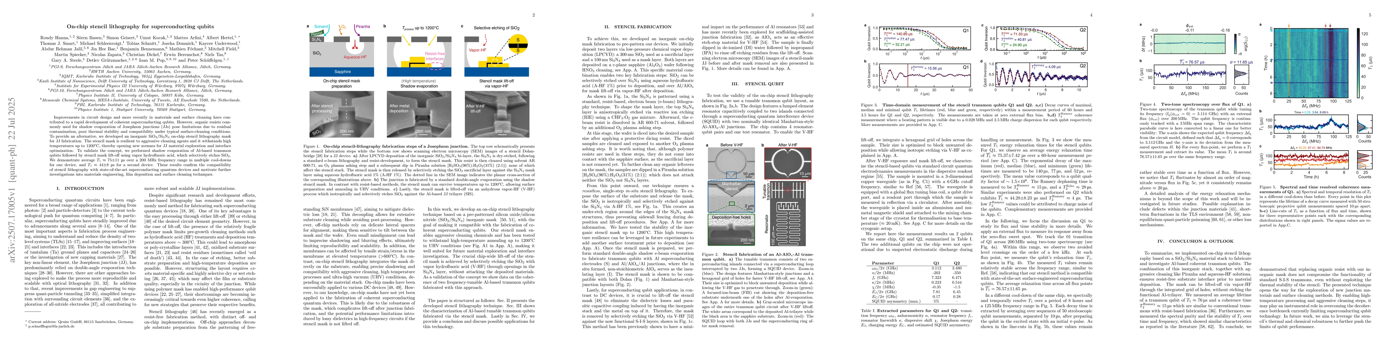
Improvements in circuit design and more recently in materials and surface cleaning have contributed to a rapid development of coherent superconducting qubits. However, organic resists commonly used fo...
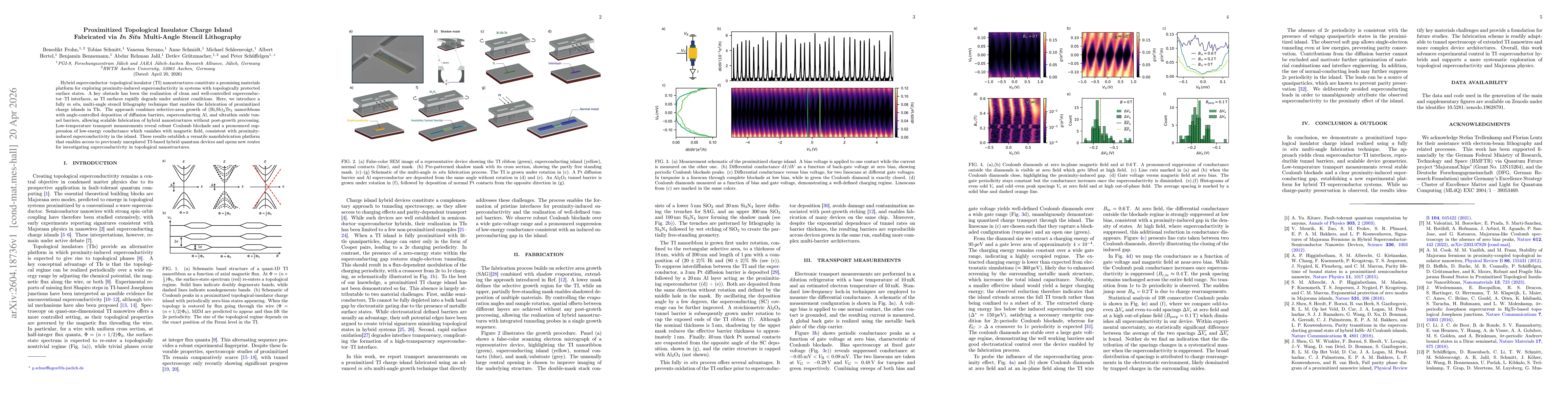
Hybrid superconductor-topological insulator (TI) nanostructures constitute a promising materials platform for exploring proximity-induced superconductivity in systems with topologically protected surf...
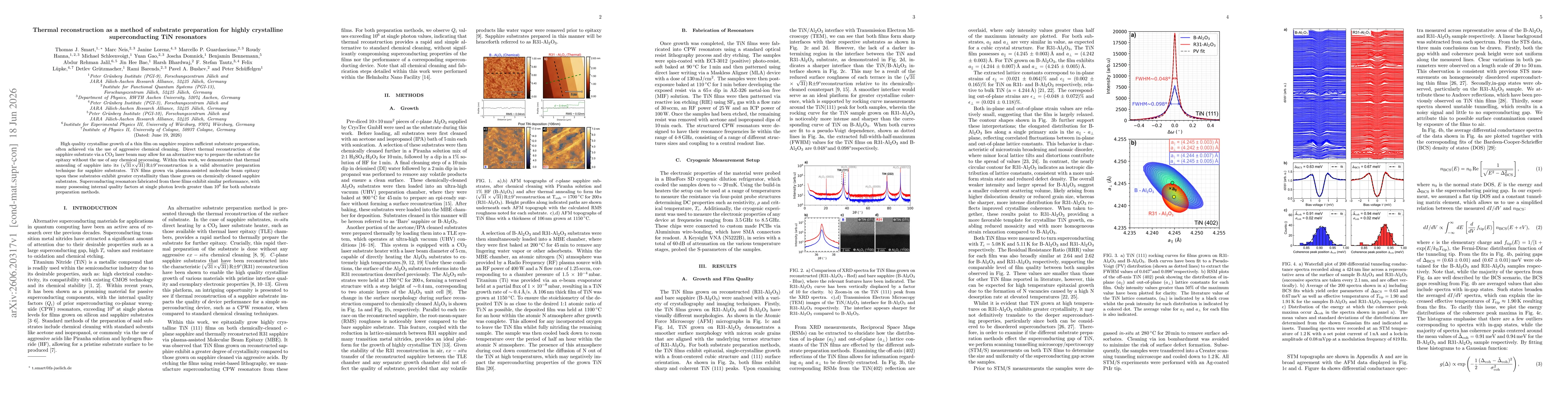
High quality crystalline growth of a thin film on sapphire requires sufficient substrate preparation, often achieved via the use of aggressive chemical cleaning. Direct thermal reconstruction of the s...