ArxivLens
B
Researcher

Benjamin Whitefield

12 papers on arXiv

12 arXiv Papers
11 Total Publications
Profile

Academic Profile

Name Benjamin Whitefield
Total Papers 11
Scholar Profile View on Semantic Scholar
Metrics

Statistics

12 arXiv Papers
11 Total Publications
Publications

Papers on arXiv

Thumbnail for Fast characterization of optically detected magnetic resonance spectra
  via data clustering
arXiv
Fast characterization of optically detected magnetic resonance spectra via data clustering

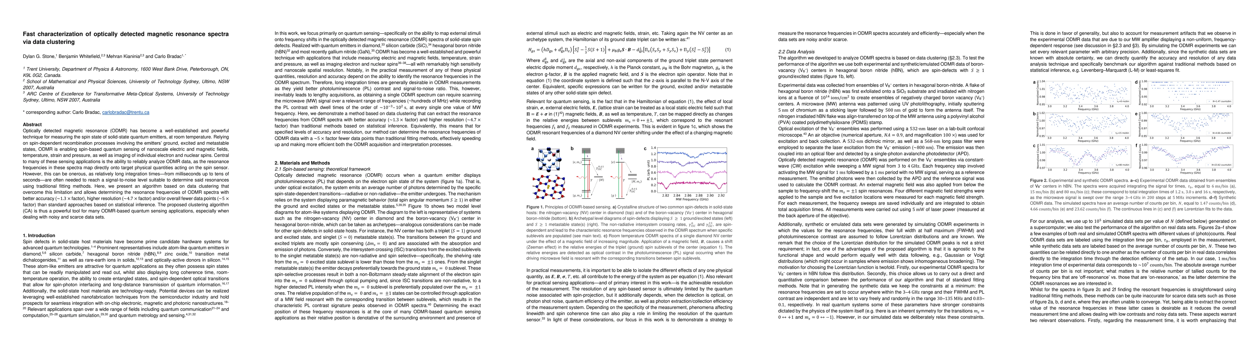
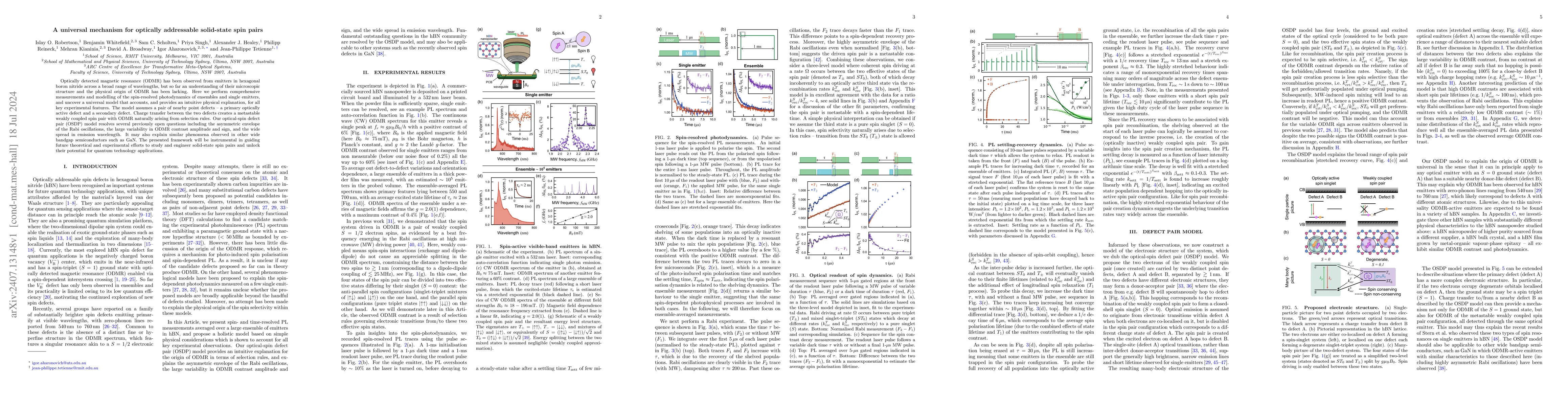
Optically detected magnetic resonance (ODMR) has become a well-established and powerful technique for measuring the spin state of solid-state quantum emitters, at room temperature. Relying on spin-d...

Thumbnail for Fibre-integrated van der Waals quantum sensor with an optimal cavity
  interface
arXiv
Fibre-integrated van der Waals quantum sensor with an optimal cavity interface

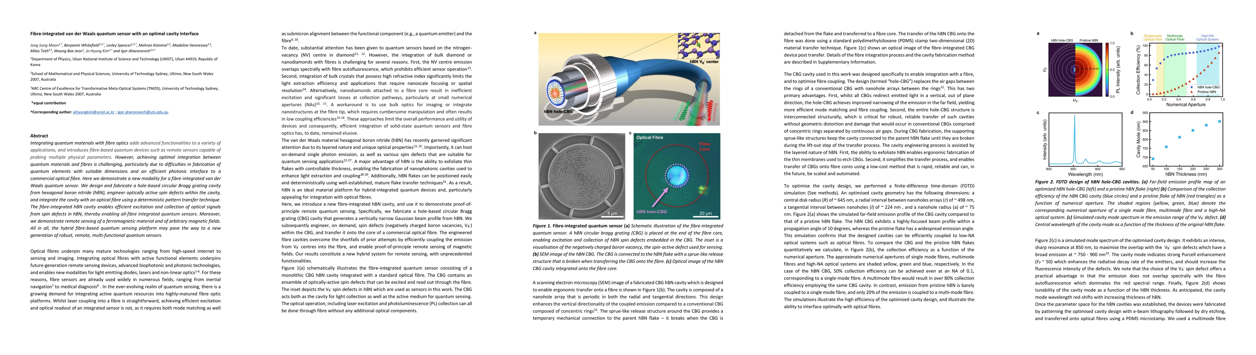
Integrating quantum materials with fibre optics adds advanced functionalities to a variety of applications, and introduces fibre-based quantum devices such as remote sensors capable of probing multi...

Thumbnail for Manipulating the Charge State of Spin Defects in Hexagonal Boron Nitride
arXiv
Manipulating the Charge State of Spin Defects in Hexagonal Boron Nitride

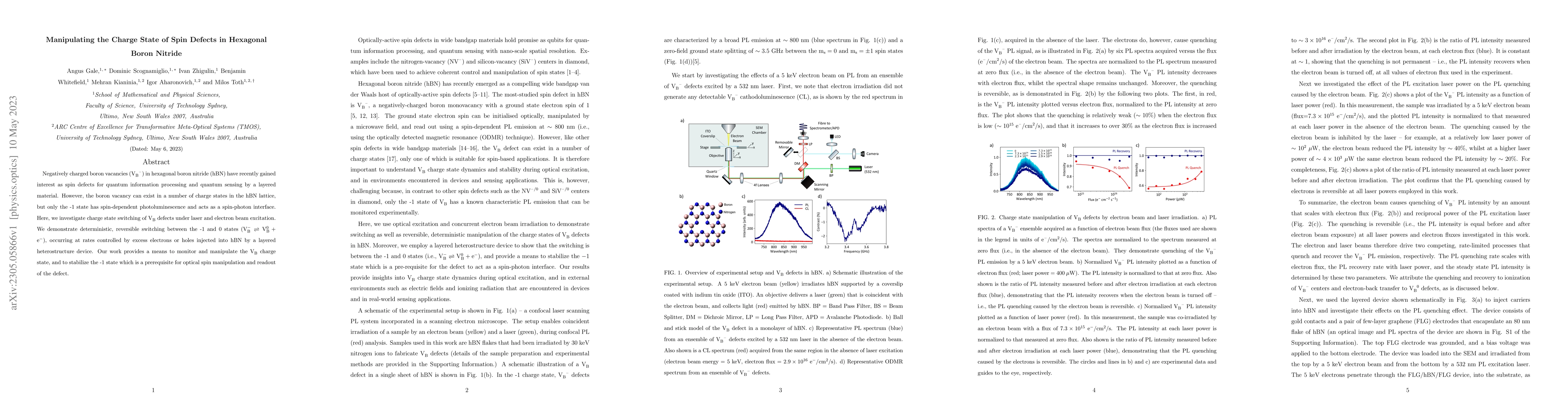
Negatively charged boron vacancies ($\small{V_B^-}$) in hexagonal boron nitride (hBN) have recently gained interest as spin defects for quantum information processing and quantum sensing by a layere...

Thumbnail for Framework for engineering of spin defects in hexagonal boron nitride by
  focused ion beams
arXiv
Framework for engineering of spin defects in hexagonal boron nitride by focused ion beams

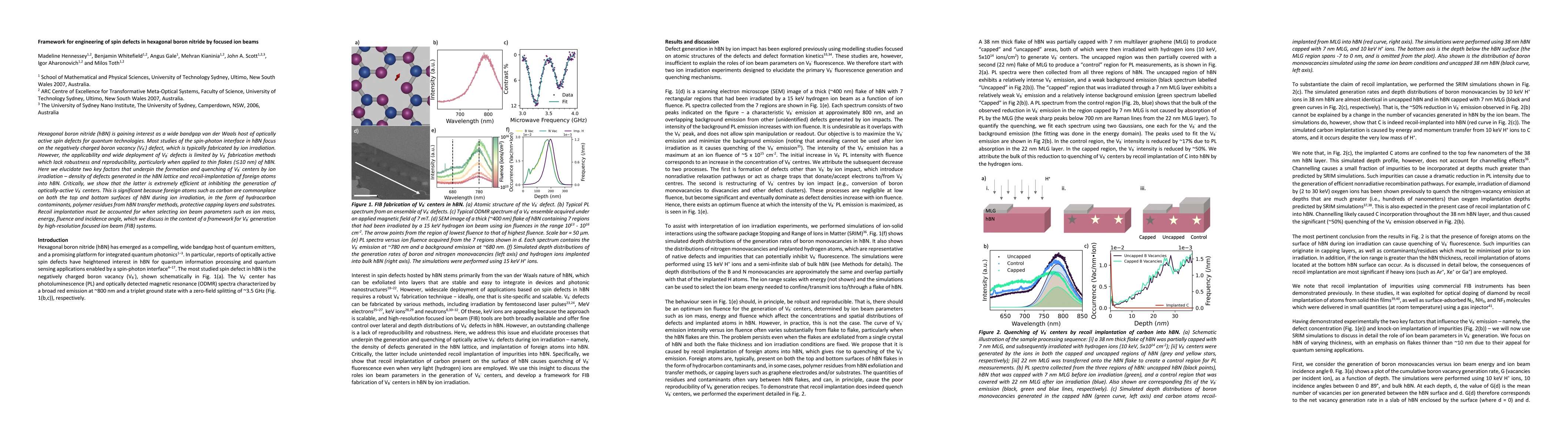
Hexagonal boron nitride (hBN) is gaining interest as a wide bandgap van der Waals host of optically active spin defects for quantum technologies. Most studies of the spin-photon interface in hBN foc...

Thumbnail for Coupling spin defects in hexagonal boron nitride to a microwave cavity
arXiv
Coupling spin defects in hexagonal boron nitride to a microwave cavity

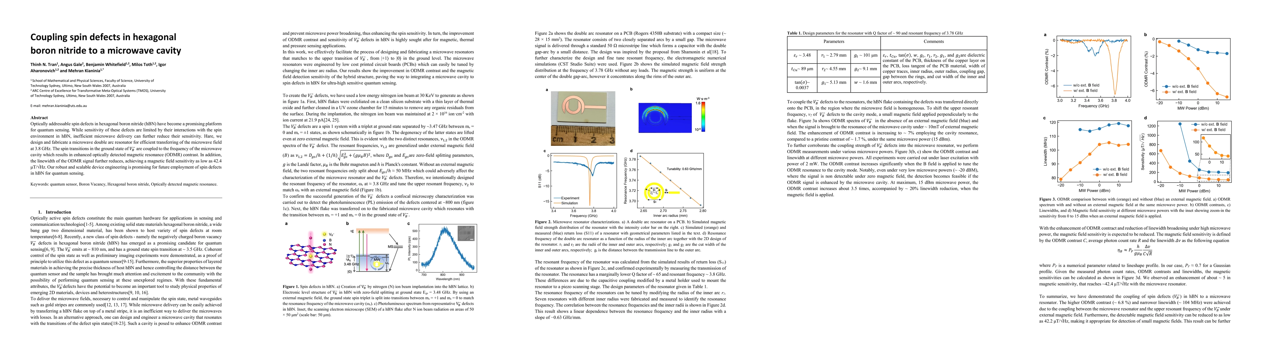
Optically addressable spin defects in hexagonal boron nitride (hBN) have become a promising platform for quantum sensing. While sensitivity of these defects are limited by their interactions with th...

Thumbnail for Double Etch Method for the Fabrication of Nanophotonic Devices from Van
  der Waals Materials
arXiv
Double Etch Method for the Fabrication of Nanophotonic Devices from Van der Waals Materials

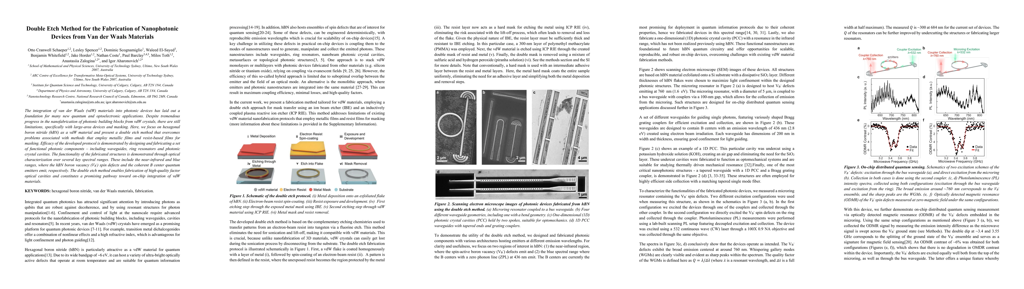
The integration of van der Waals (vdW) materials into photonic devices has laid out a foundation for many new quantum and optoelectronic applications. Despite tremendous progress in the nanofabricatio...

Thumbnail for A universal mechanism for optically addressable solid-state spin pairs
arXiv
A universal mechanism for optically addressable solid-state spin pairs

Optically detected magnetic resonance (ODMR) has been observed from emitters in hexagonal boron nitride across a broad range of wavelengths, but so far an understanding of their microscopic structure ...

Thumbnail for Generation of narrowband quantum emitters in hBN with optically
  addressable spins
arXiv
Generation of narrowband quantum emitters in hBN with optically addressable spins

Electron spins coupled with optical transitions in solids stand out as a promising platform for developing spin-based quantum technologies. Recently, hexagonal boron nitride (hBN) - a layered Van der ...

Thumbnail for Photodynamics and Temperature Dependence of Single Spin Defects in Hexagonal Boron Nitride
arXiv
Photodynamics and Temperature Dependence of Single Spin Defects in Hexagonal Boron Nitride

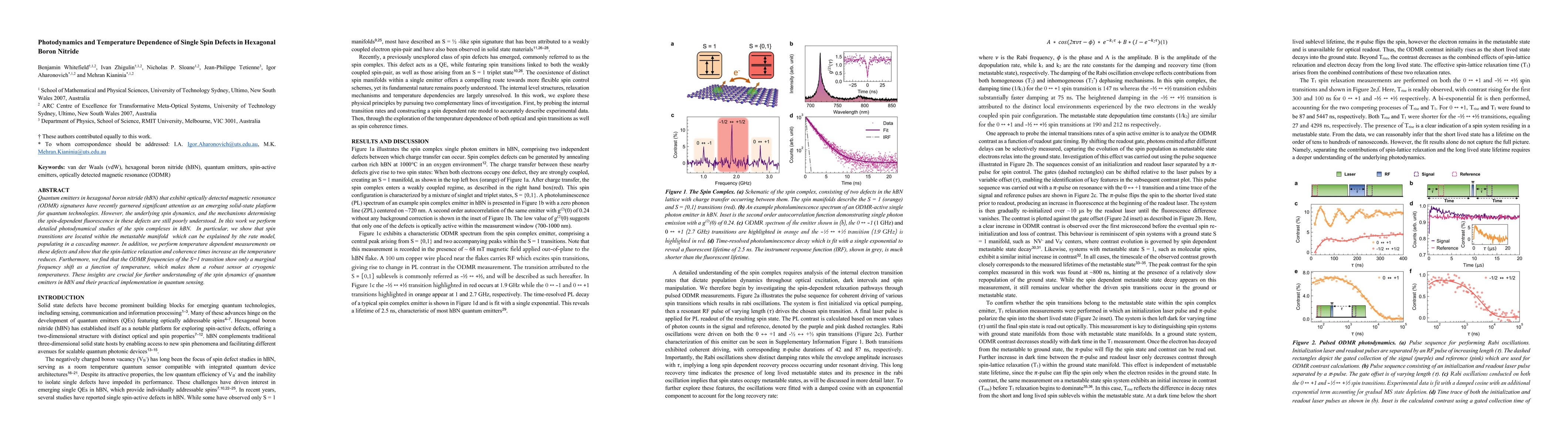
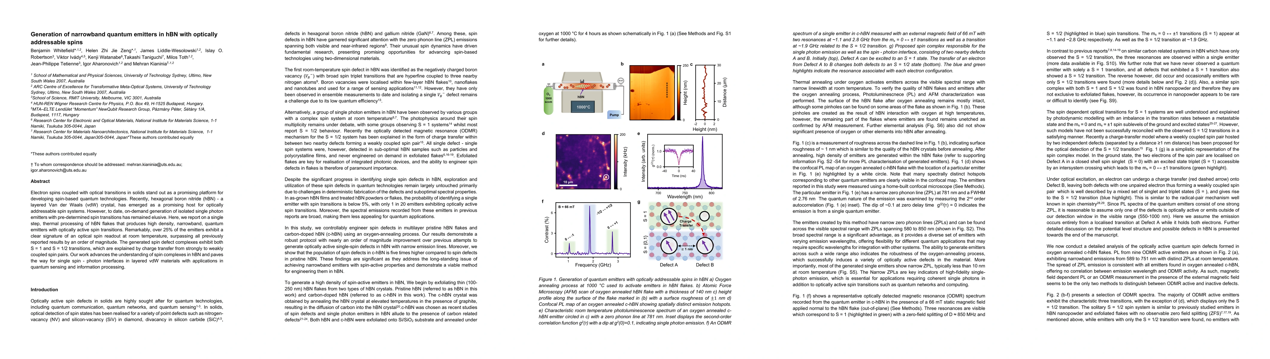
Quantum emitters in hexagonal boron nitride (hBN) that exhibit optically detected magnetic resonance (ODMR) signatures have recently garnered significant attention as an emerging solid-state platform ...

Thumbnail for Deterministic integration of quantum emitters and optical cavities in a van der Waals crystal
arXiv
Deterministic integration of quantum emitters and optical cavities in a van der Waals crystal

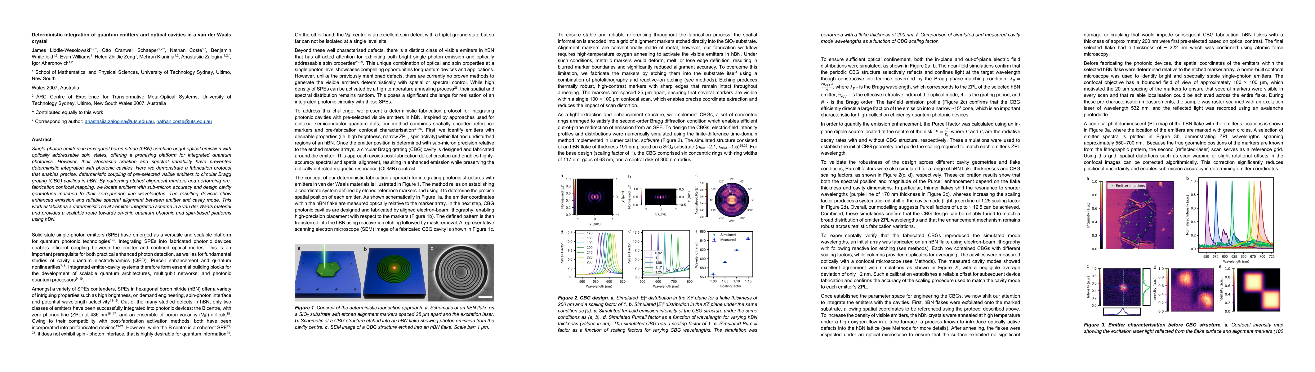
Single-photon emitters in hexagonal boron nitride (hBN) combine bright optical emission with optically addressable spin states, offering a promising platform for integrated quantum photonics. However,...

Thumbnail for Multi-wavelength Spin Dynamics of Defects in Hexagonal Boron Nitride
arXiv
Multi-wavelength Spin Dynamics of Defects in Hexagonal Boron Nitride

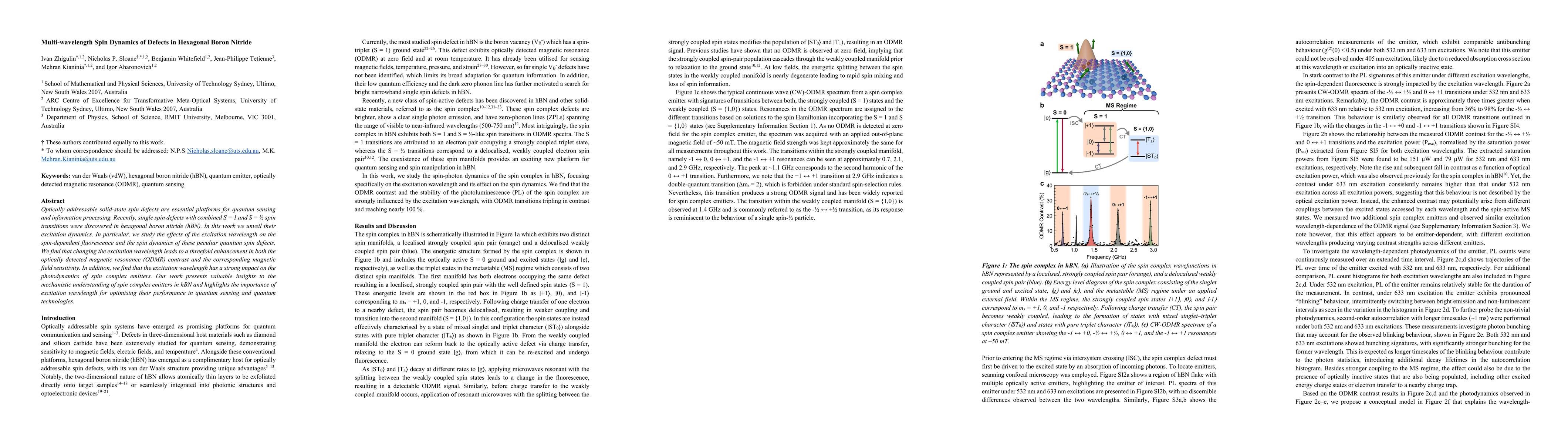
Optically addressable solid-state spin defects are essential platforms for quantum sensing and information processing. Recently, single spin defects with combined S = 1 and S = 1/2 spin transitions we...

Thumbnail for On chip, multifunctional quantum sensing using single spins in a van der Waals crystal
arXiv
On chip, multifunctional quantum sensing using single spins in a van der Waals crystal

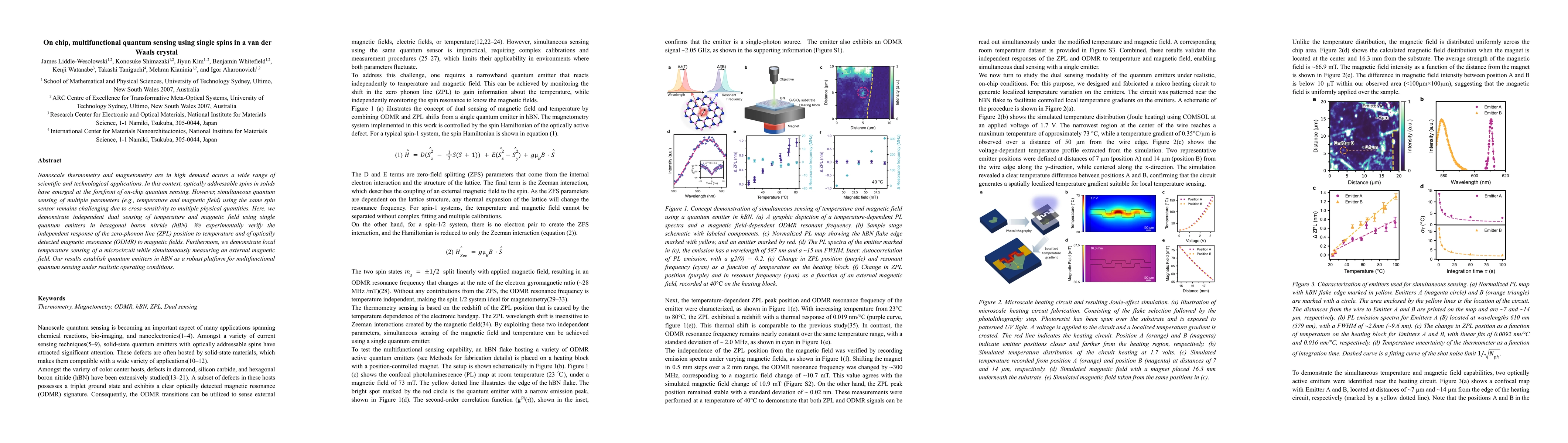
Nanoscale thermometry and magnetometry are in high demand across a wide range of scientific and technological applications. In this context, optically addressable spins in solids have emerged at the f...

This website uses cookies to ensure you get the best experience. Learn more