Academic Profile
Statistics
Similar Authors
Papers on arXiv
The role of defects in two-dimensional semiconductors and how they affect the intrinsic properties of these materials have been a wide researched topic over the past decades. Optical characterizatio...
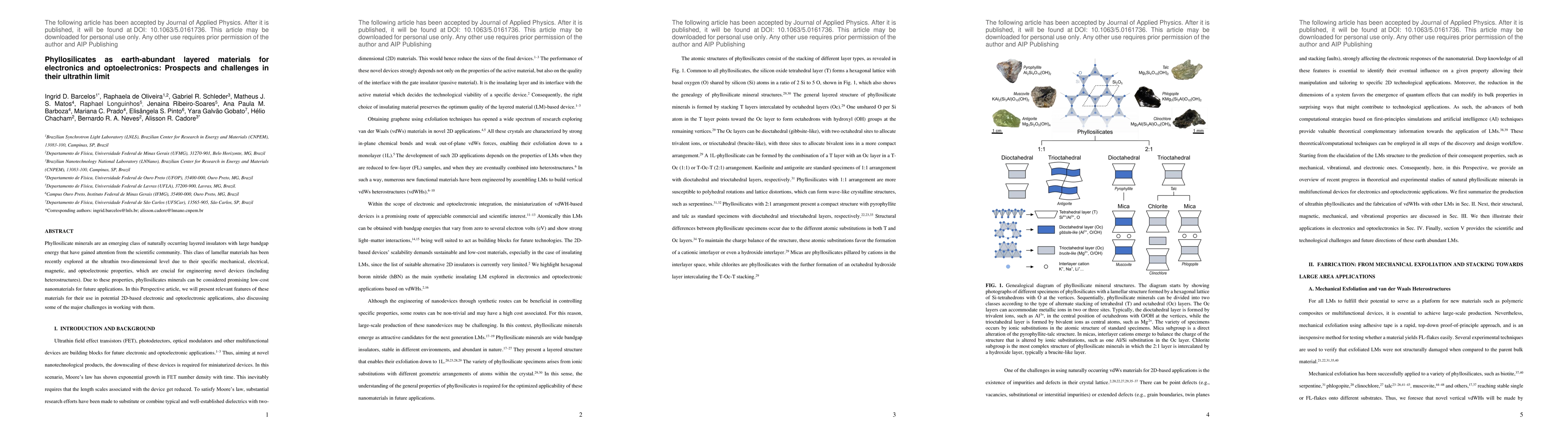
Phyllosilicate minerals are an emerging class of naturally occurring layered insulators with large bandgap energy that have gained attention from the scientific community. This class of lamellar mat...
The new generation of two-dimensional (2D) materials has shown a broad range of applications for optical and electronic devices. Understanding the properties of these materials when integrated with ...
Contaminations in the formation of two-dimensional heterostructures can hinder or generate desired properties. Recent advancements have highlighted the potential of tip-enhanced Raman spectroscopy (TE...
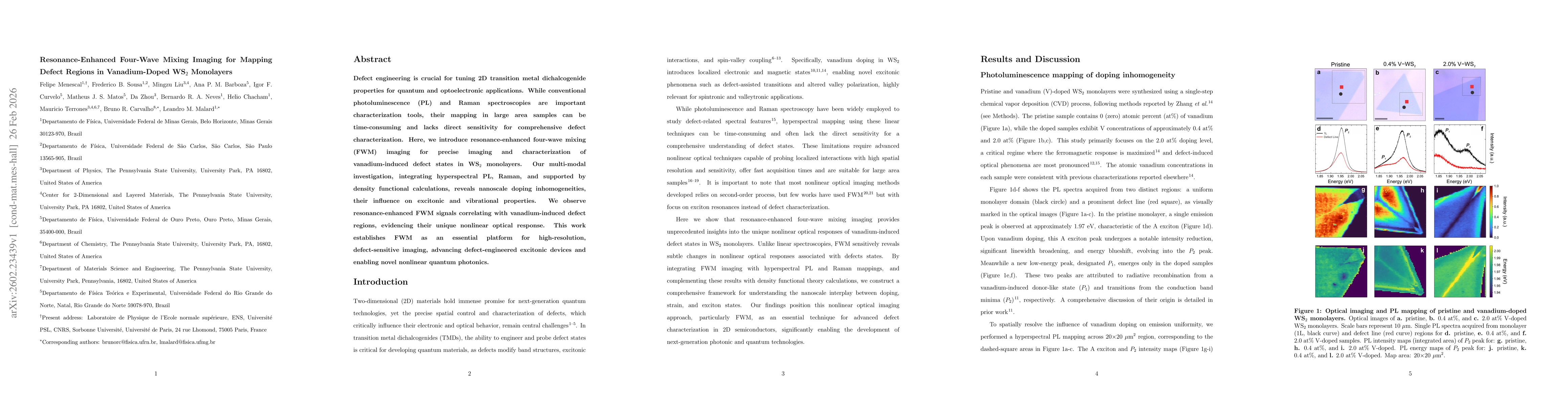
Defect engineering is crucial for tuning 2D transition metal dichalcogenide properties for quantum and optoelectronic applications. While conventional photoluminescence (PL) and Raman spectroscopies a...