Academic Profile
Statistics
Similar Authors
Papers on arXiv
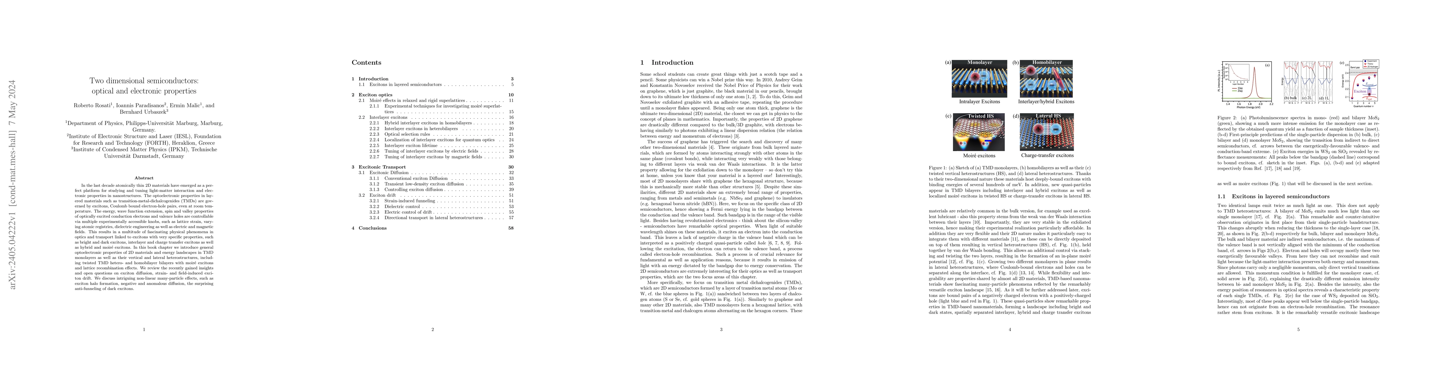
In the last decade atomically thin 2D materials have emerged as a perfect platform for studying and tuning light-matter interaction and electronic properties in nanostructures. The optoelectronic pr...
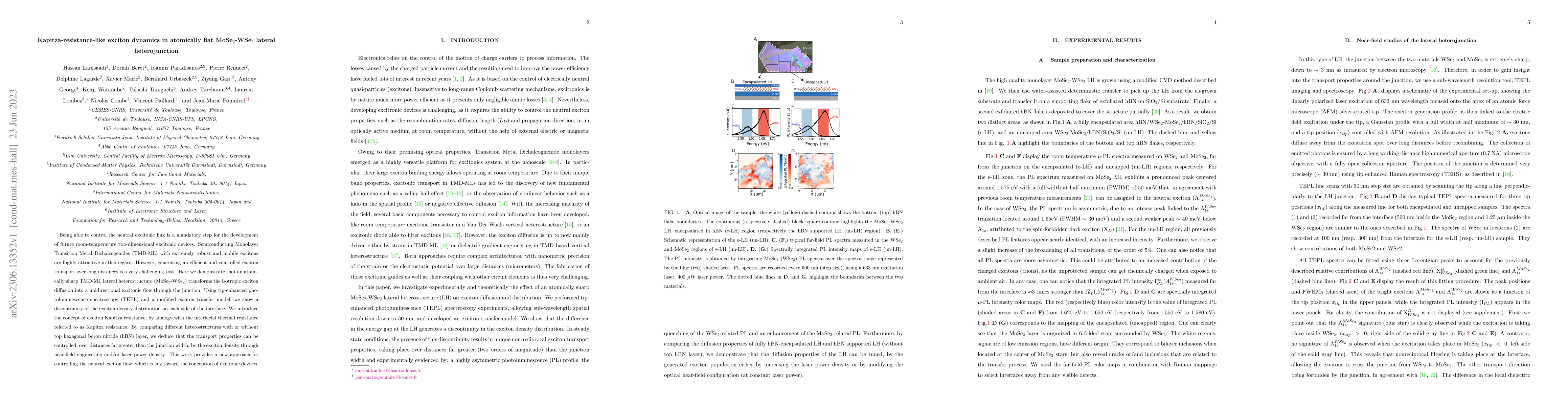
Being able to control the neutral excitonic flux is a mandatory step for the development of future room-temperature two-dimensional excitonic devices. Semiconducting Monolayer Transition Metal Dicha...
The existence of bound charge transfer (CT) excitons at the interface of monolayer lateral heterojunctions has been debated in literature, but contrary to the case of interlayer excitons in vertical...
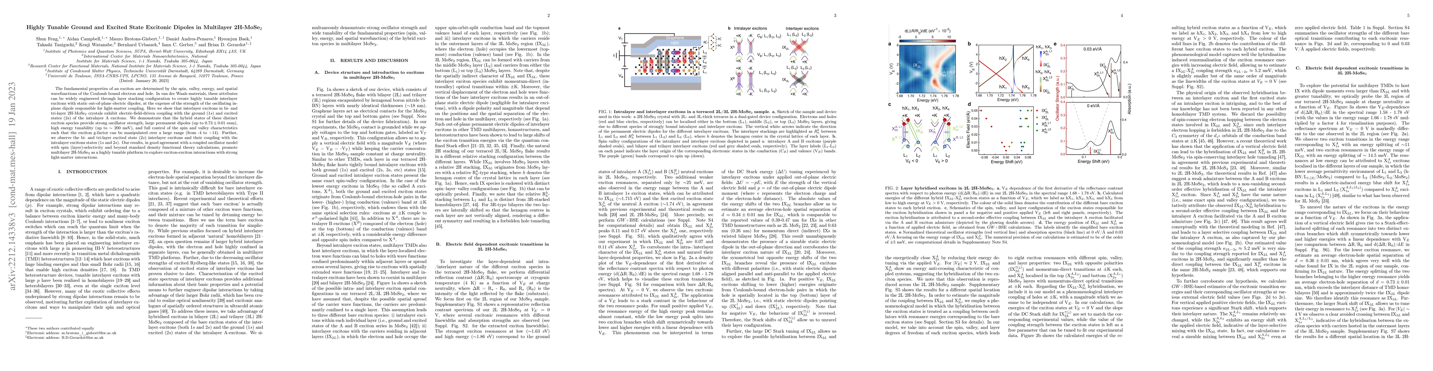
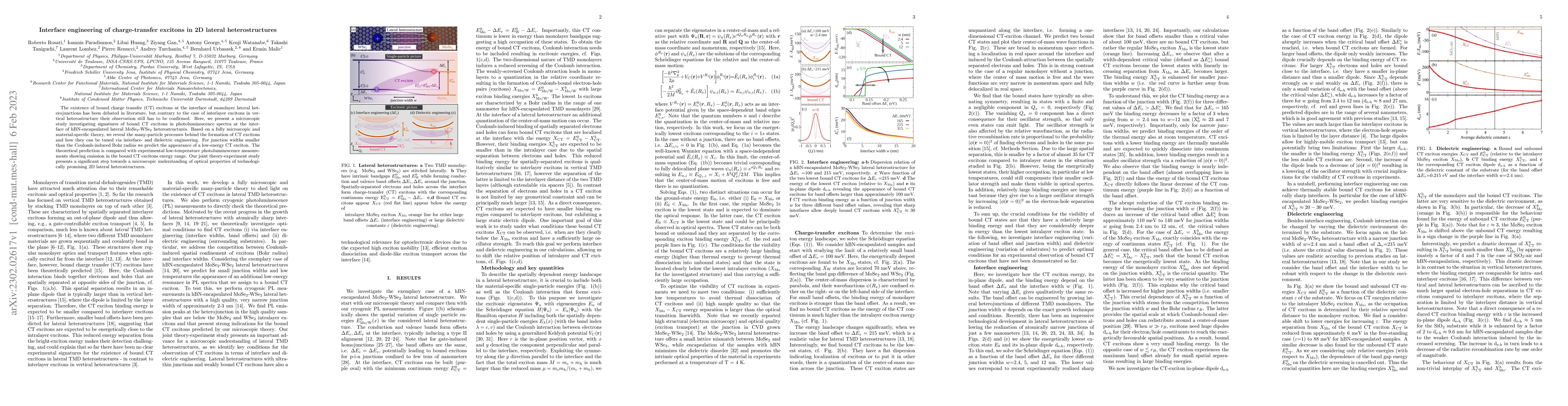
The fundamental properties of an exciton are determined by the spin, valley, energy, and spatial wavefunctions of the Coulomb bound electron and hole. In van der Waals materials, these attributes ca...
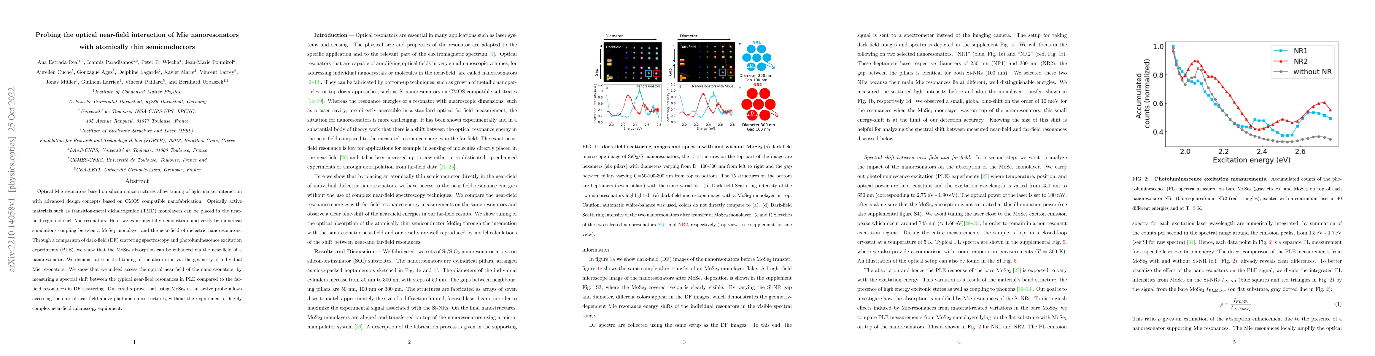
Optical Mie resonators based on silicon nanostructures allow tuning of light-matter-interaction with advanced design concepts based on CMOS compatible nanofabrication. Optically active materials suc...
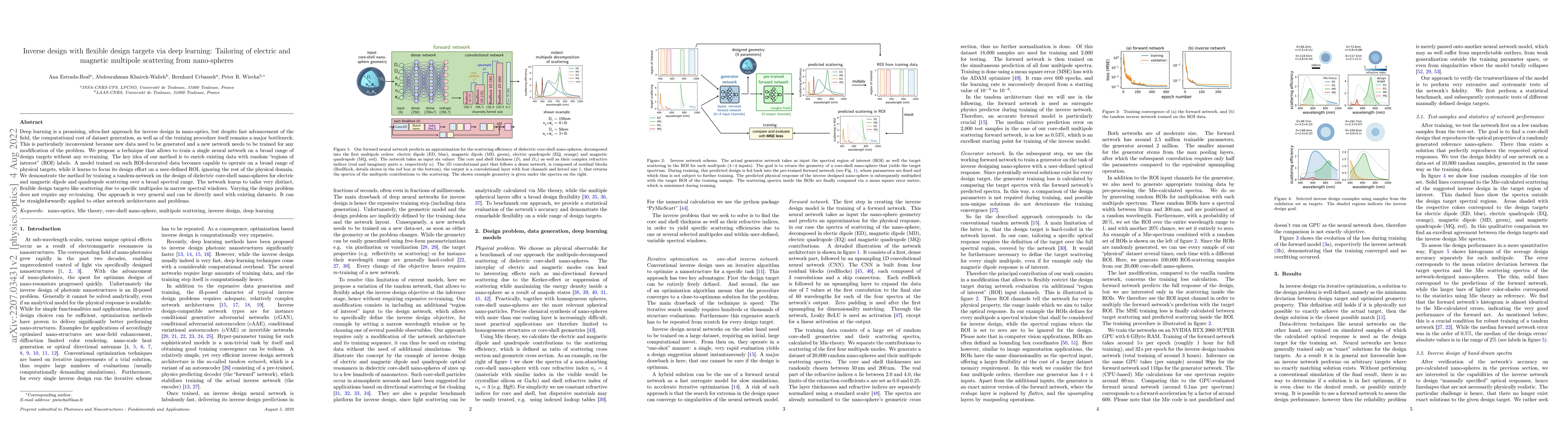
Deep learning is a promising, ultra-fast approach for inverse design in nano-optics, but despite fast advancement of the field, the computational cost of dataset generation, as well as of the traini...
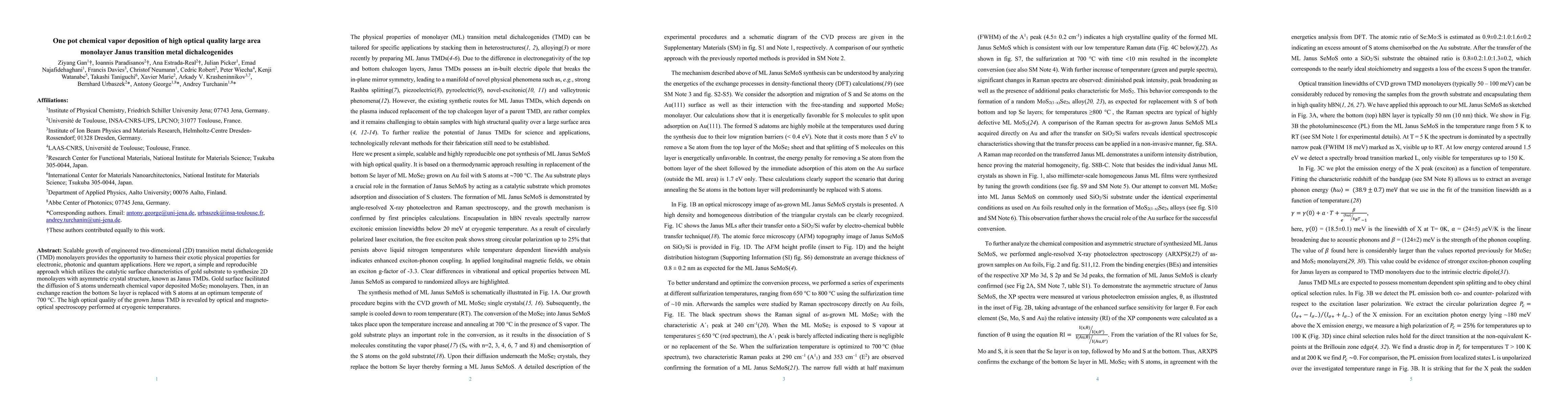
We report one-pot chemical vapor deposition (CVD) growth of large-area Janus SeMoS monolayers, with the asymmetric top (Se) and bottom (S) chalcogen atomic planes with respect to the central transit...
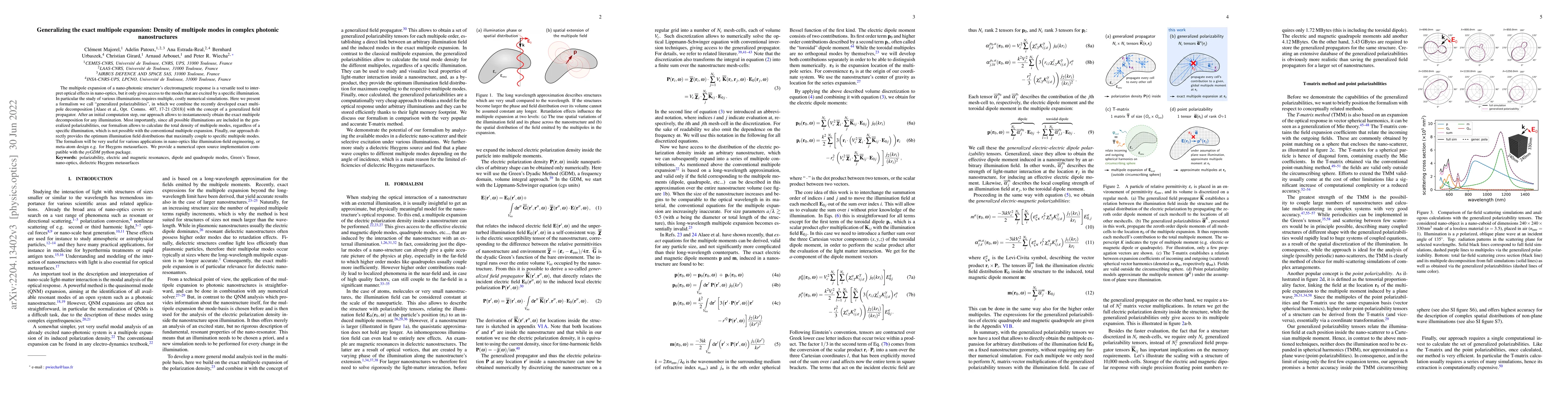
The multipole expansion of a nano-photonic structure's electromagnetic response is a versatile tool to interpret optical effects in nano-optics, but it only gives access to the modes that are excite...
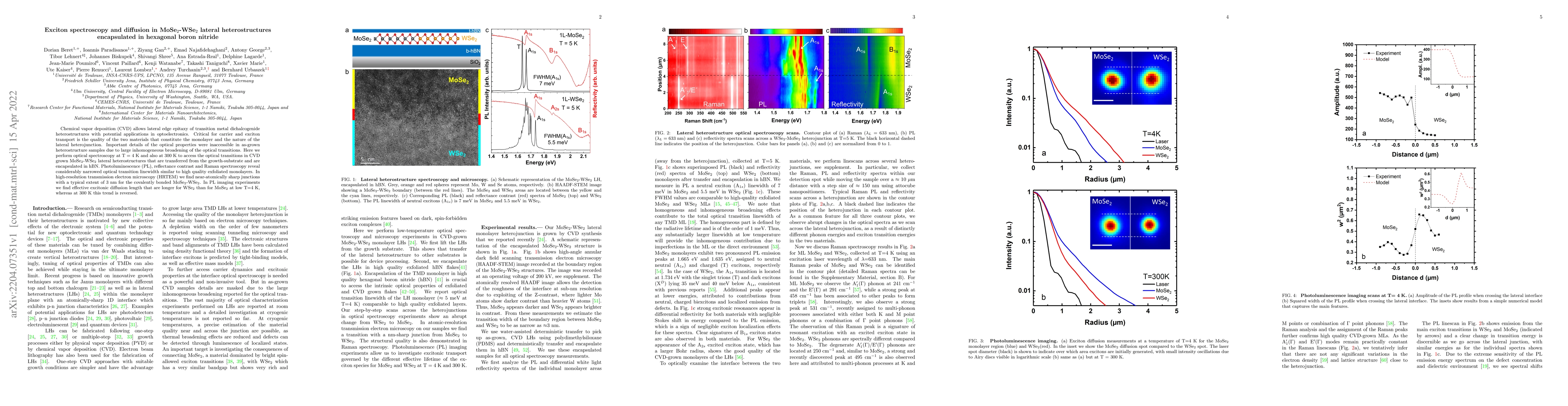
Chemical vapor deposition (CVD) allows lateral edge epitaxy of transition metal dichalcogenide heterostructures with potential applications in optoelectronics. Critical for carrier and exciton trans...
Using a spatially-resolved optical pump-probe experiment, we measure the lateral transport of spin/valley polarized electrons over very long distances (tens of micrometers) in a single WSe2 monolaye...
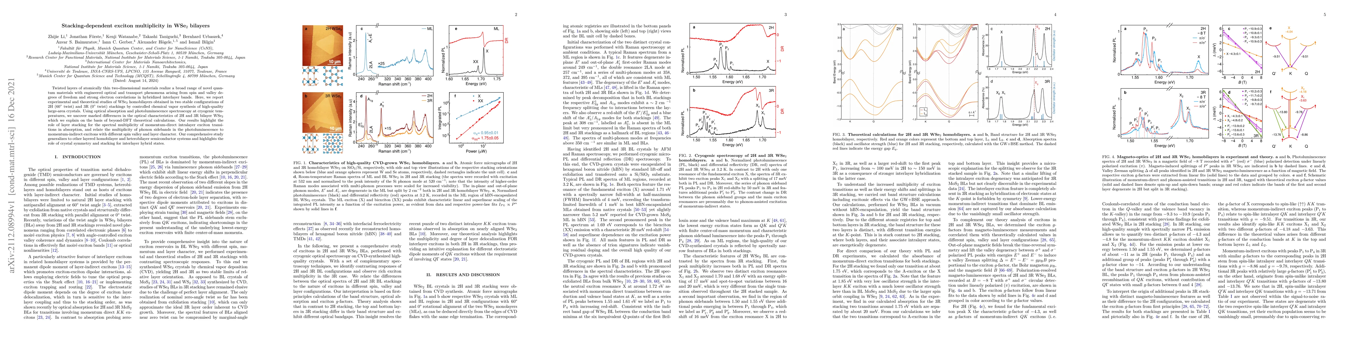
Twisted layers of atomically thin two-dimensional materials realize a broad range of novel quantum materials with engineered optical and transport phenomena arising from spin and valley degrees of f...
The twist angle in transition metal dichalcogenide (TMD) heterobilayers is a compelling degree of freedom that determines electron correlations and the period of lateral confinement of moir\'e excit...
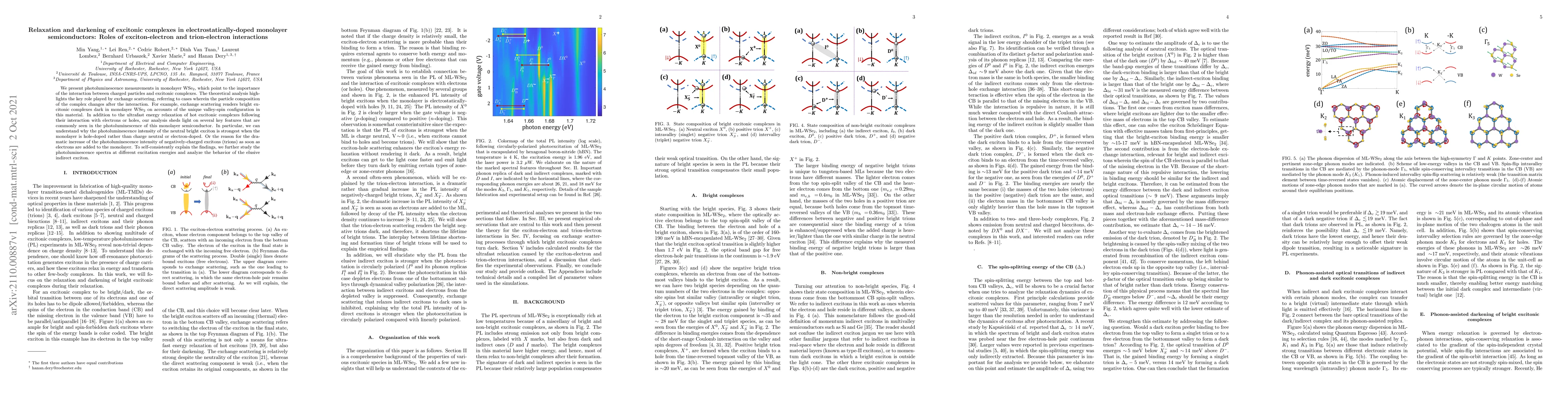
We present photoluminescence measurements in monolayer WSe$_2$, which point to the importance of the interaction between charged particles and excitonic complexes. The theoretical analysis highlight...
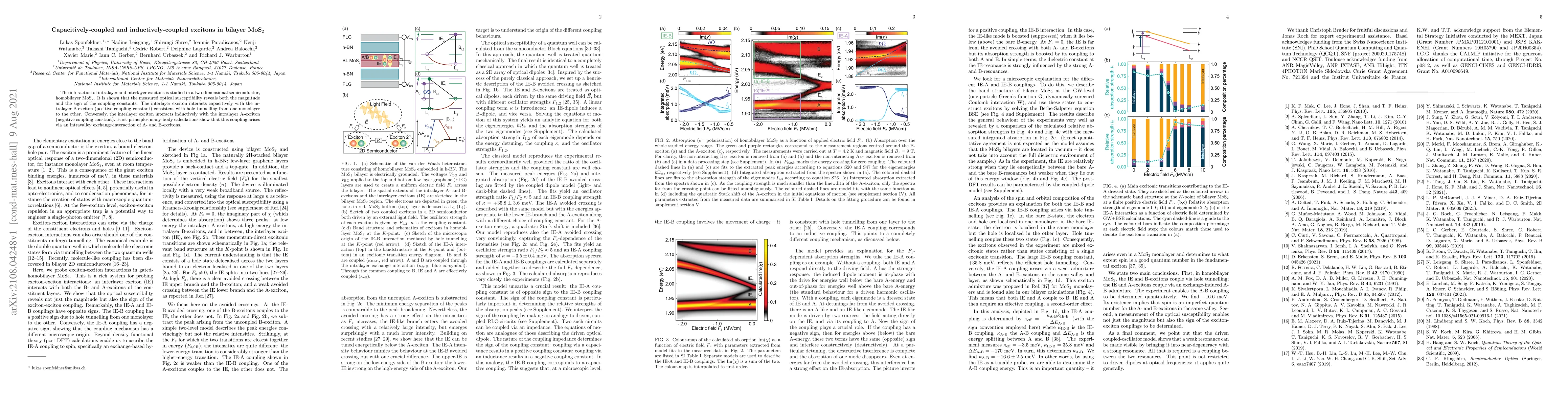
The interaction of intralayer and interlayer excitons is studied in a two-dimensional semiconductor, homobilayer MoS$_2$. It is shown that the measured optical susceptibility reveals both the magnit...
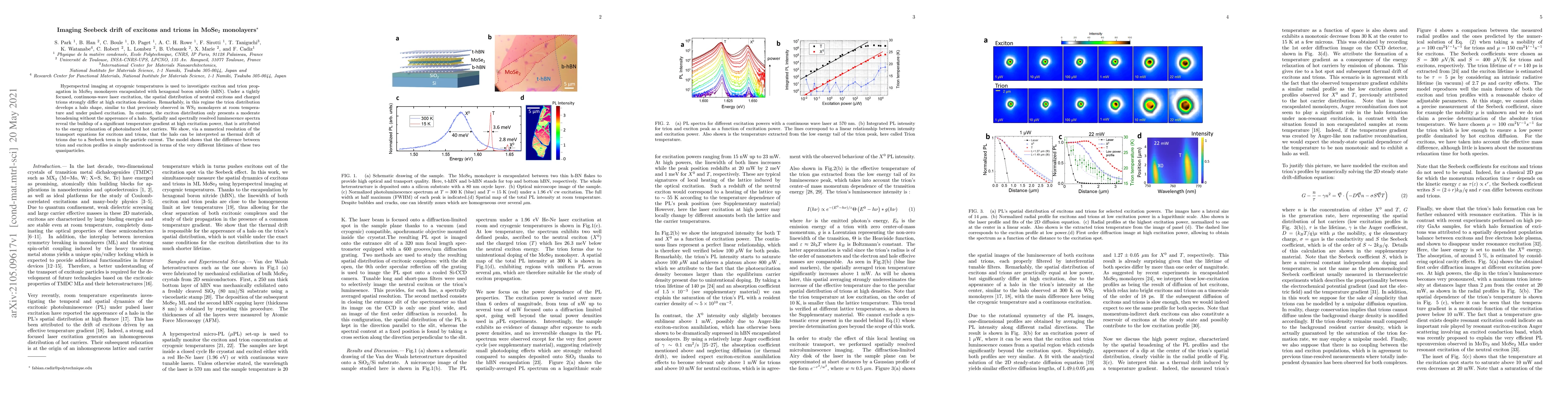
Hyperspectral imaging at cryogenic temperatures is used to investigate exciton and trion propagation in MoSe$_2$ monolayers encapsulated with hexagonal boron nitride (hBN). Under a tightly focused, ...
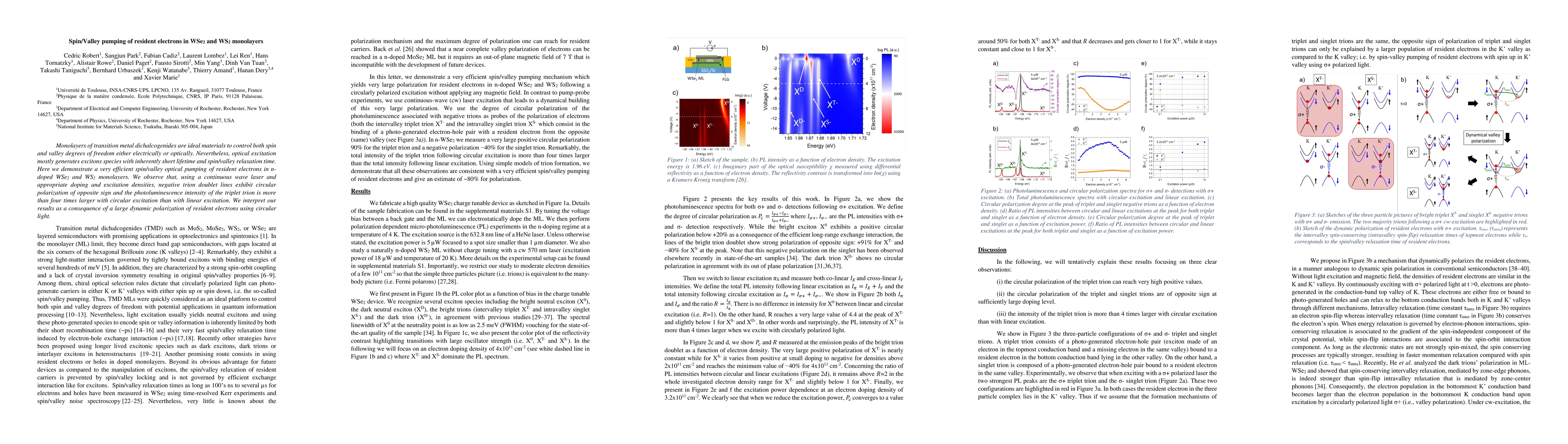
Monolayers of transition metal dichalcogenides are ideal materials to control both spin and valley degrees of freedom either electrically or optically. Nevertheless, optical excitation mostly genera...
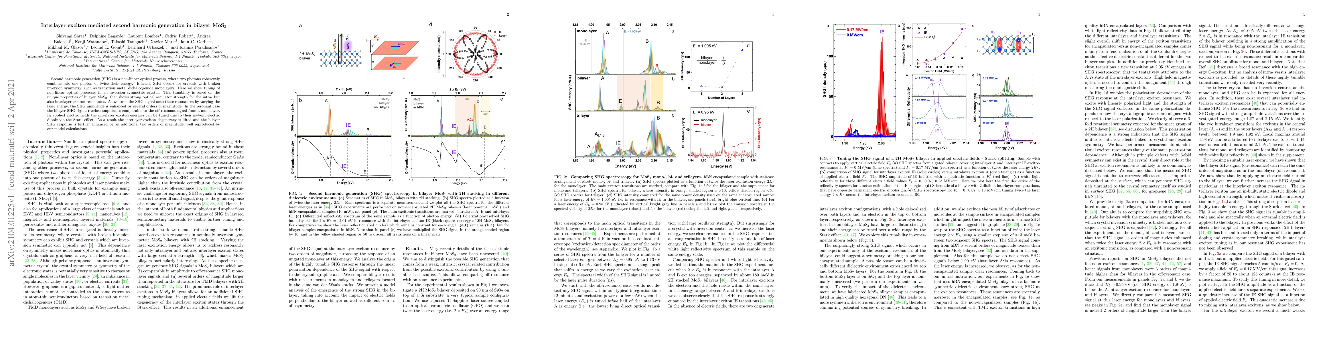
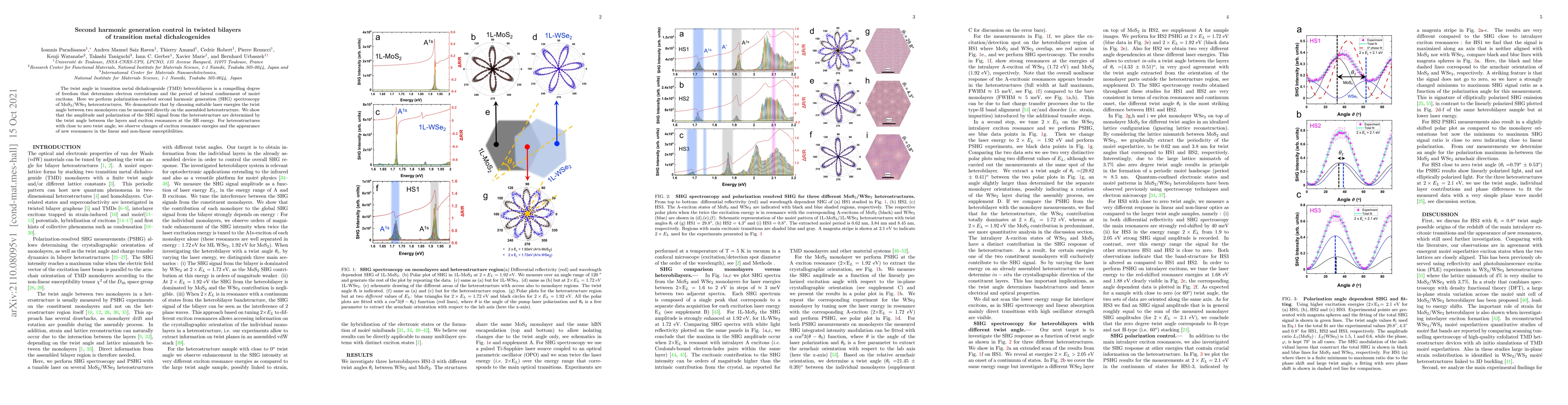
Second harmonic generation (SHG) is a non-linear optical process, where two photons coherently combine into one photon of twice their energy. Efficient SHG occurs for crystals with broken inversion ...
Monolayers of transition metal dichalcogenides (TMDs) have recently emerged as a promising optoelectronic platform. To leverage their full potential, however, it is important to understand and engin...
The electron valley and spin degree of freedom in monolayer transition-metal dichalcogenides can be manipulated in optical and transport measurements performed in magnetic fields. The key parameter ...
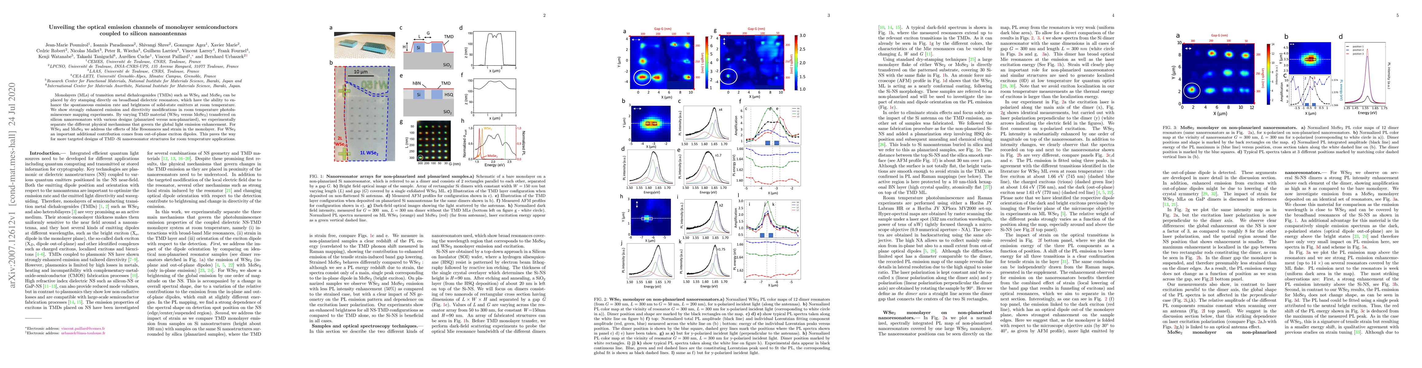
Monolayers (MLs) of transition metal dichalcogenides (TMDs) such as WSe2 and MoSe2 can be placed by dry stamping directly on broadband dielectric resonators, which have the ability to enhance the sp...
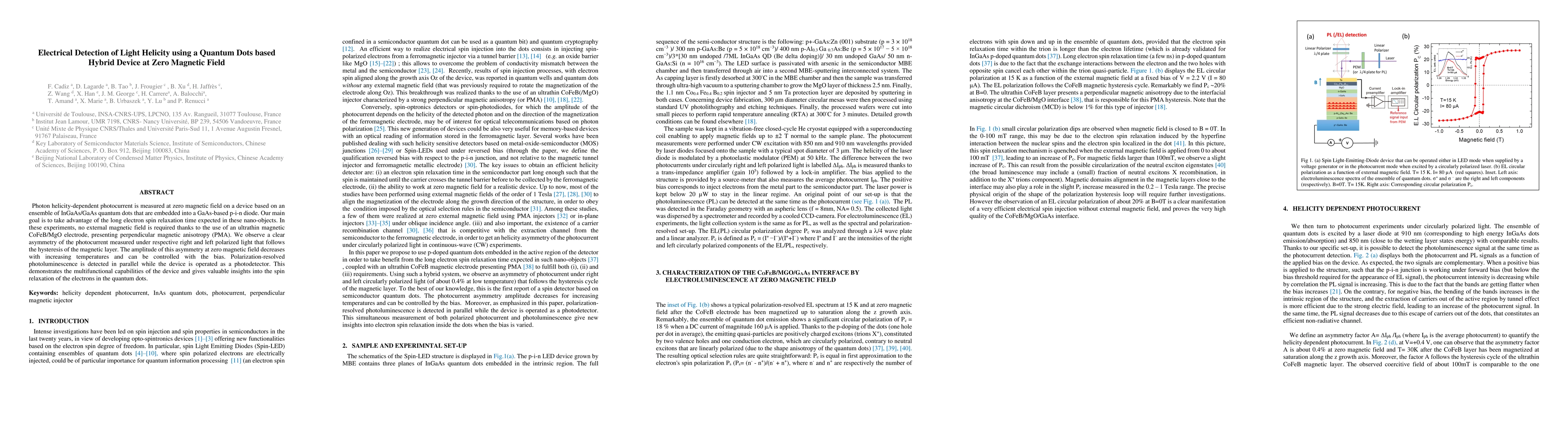
Photon helicity-dependent photocurrent is measured at zero magnetic field on a device based on an ensemble of InGaAs/GaAs quantum dots that are embedded into a GaAs-based p-i-n diode. Our main goal ...
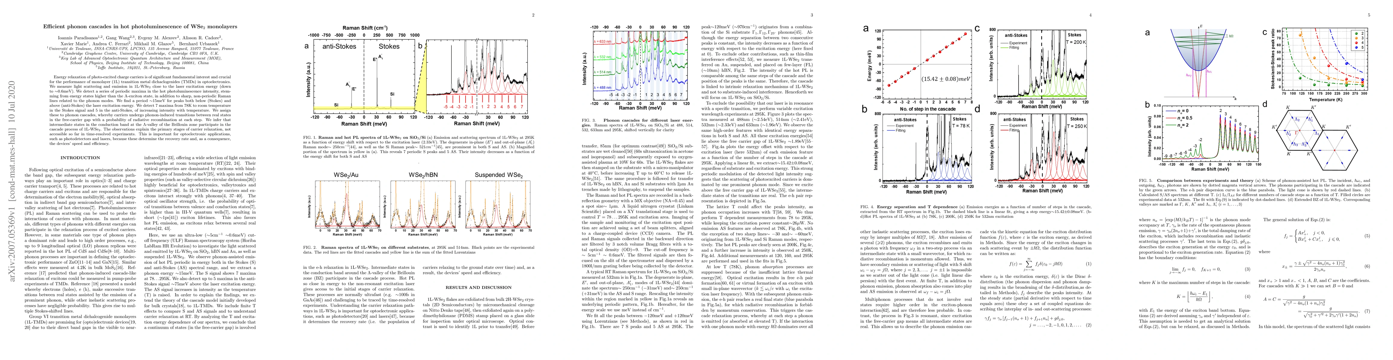
Energy relaxation of photo-excited charge carriers is of significant fundamental interest and crucial for the performance of monolayer (1L) transition metal dichaclogenides (TMDs) in optoelectronics...
In this technical review we give an introduction to optical spectroscopy for layered materials as a powerful, non-invasive tool to access details of the electronic band structure and crystal quality...
Transition metal dichalcogenides (TMDs) constitute a versatile platform for atomically thin optoelectronics devices and spin-valley memory applications. In monolayers optical absorption is strong, b...
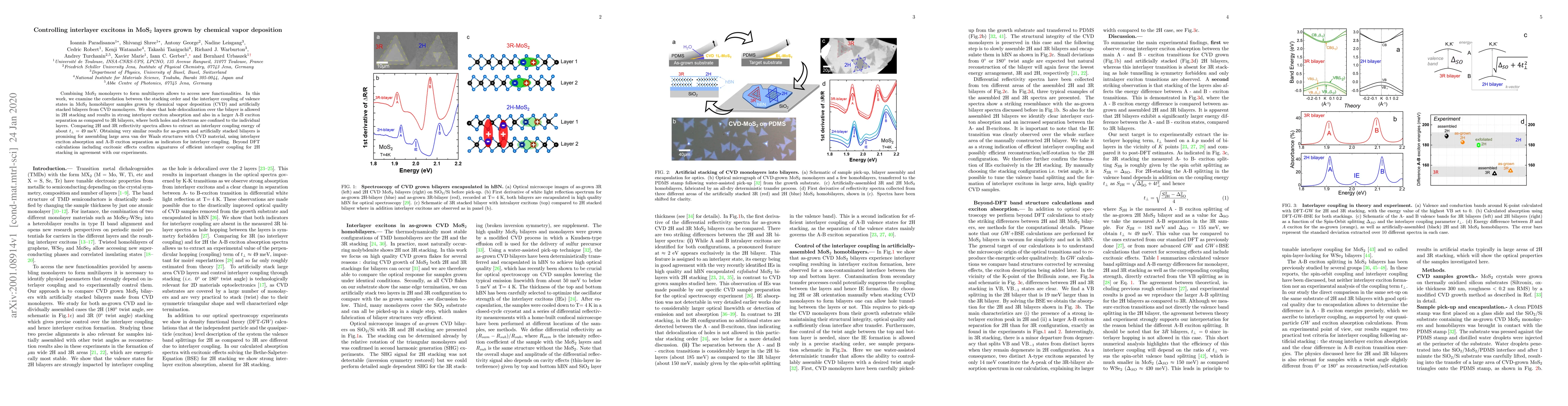
Combining MoS$_2$ monolayers to form multilayers allows to access new functionalities. In this work, we examine the correlation between the stacking order and the interlayer coupling of valence stat...
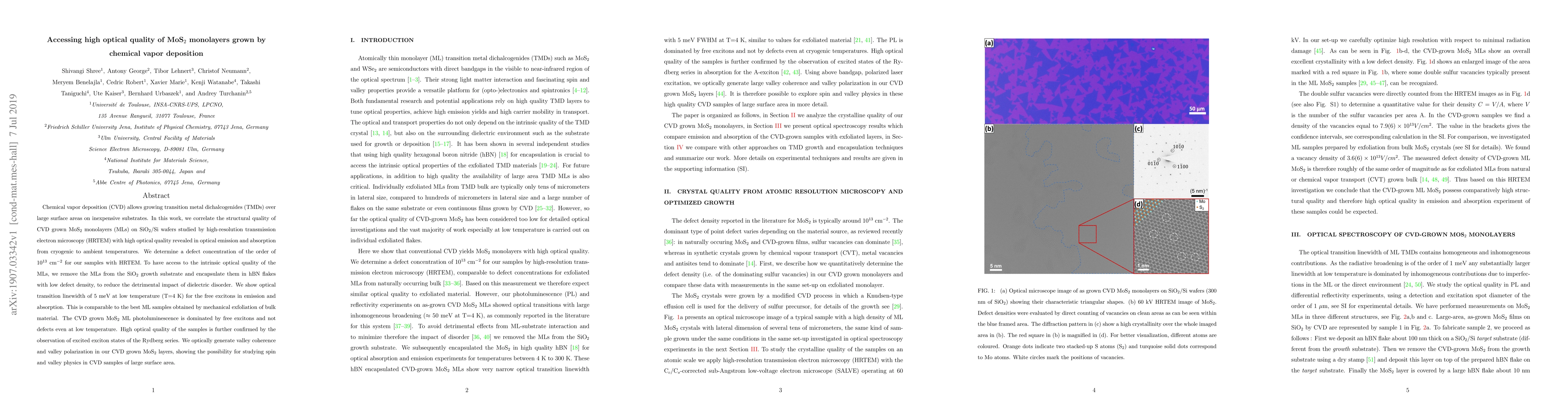
Chemical vapor deposition (CVD) allows growing transition metal dichalcogenides (TMDs) over large surface areas on inexpensive substrates. In this work, we correlate the structural quality of CVD gr...
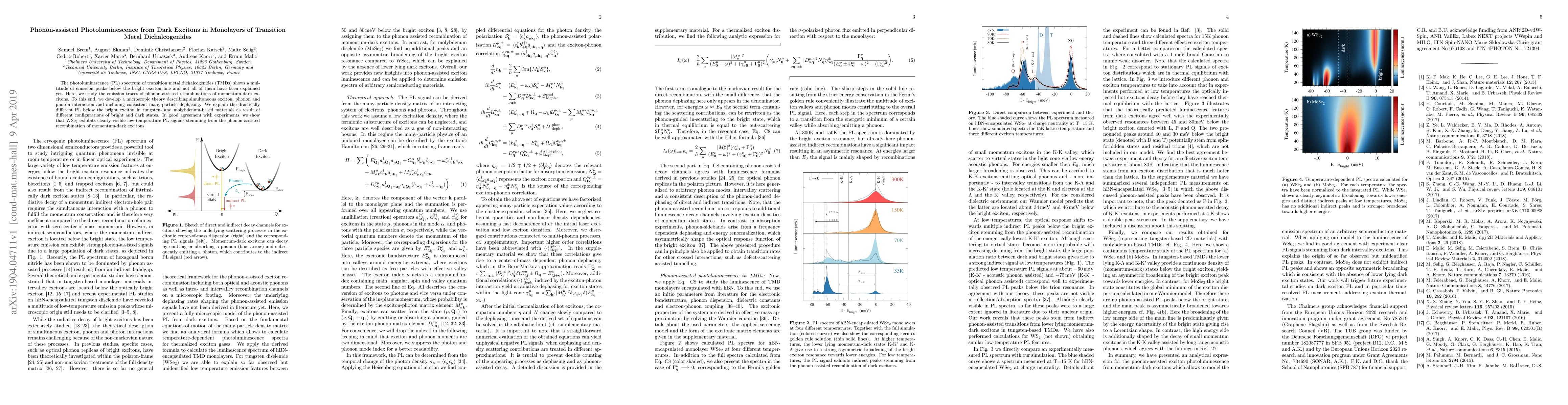
The photoluminescence (PL) spectrum of transition metal dichalcogenides (TMDs) shows a multitude of emission peaks below the bright exciton line and not all of them have been explained yet. Here, we...
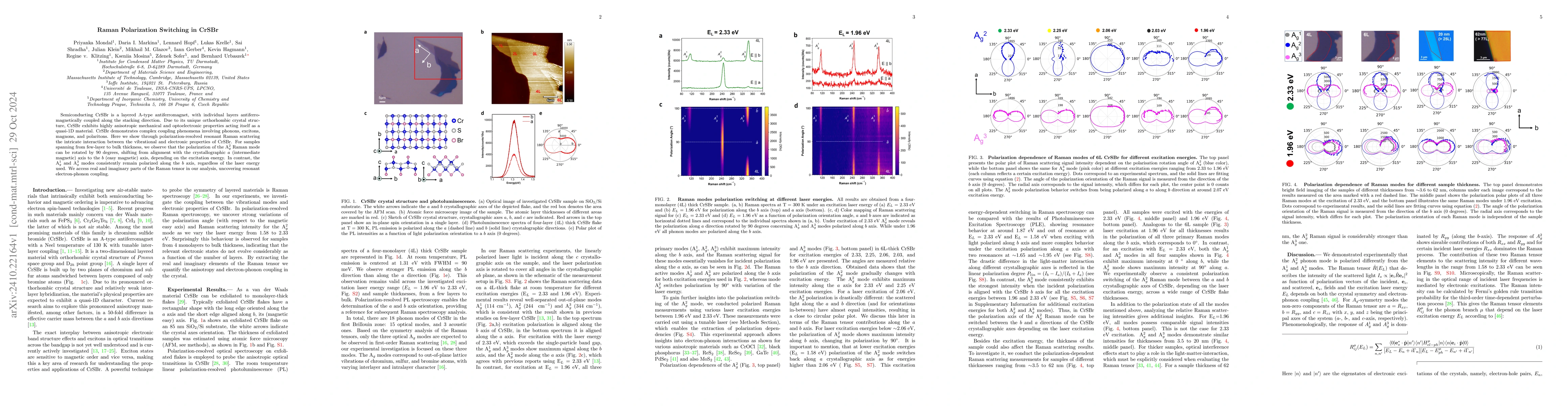
Semiconducting CrSBr is a layered A-type antiferromagnet, with individual layers antiferromagnetically coupled along the stacking direction. Due to its unique orthorhombic crystal structure, CrSBr exh...
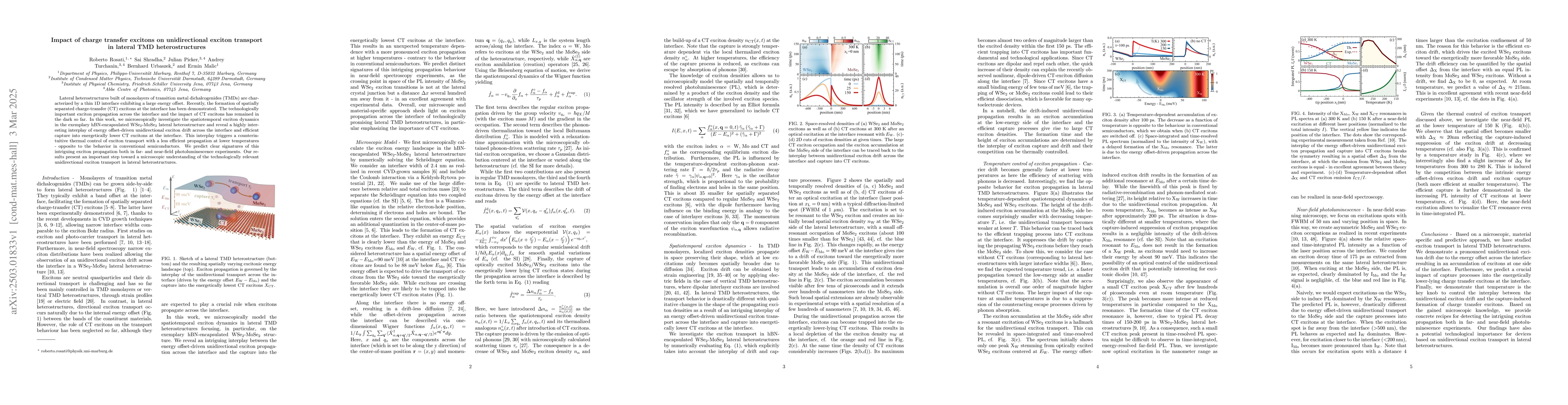
Lateral heterostructures built of monolayers of transition metal dichalcogenides (TMDs) are characterized by a thin 1D interface exhibiting a large energy offset. Recently, the formation of spatially ...
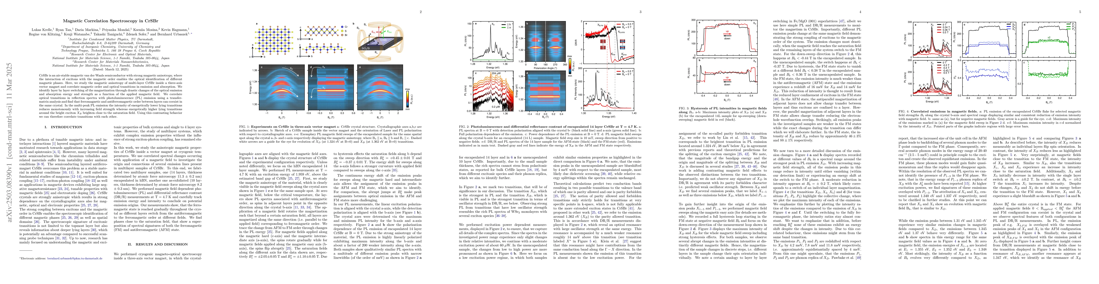
CrSBr is an air-stable magnetic van der Waals semiconductor with strong magnetic anisotropy, where the interaction of excitons with the magnetic order enables the optical identification of different m...
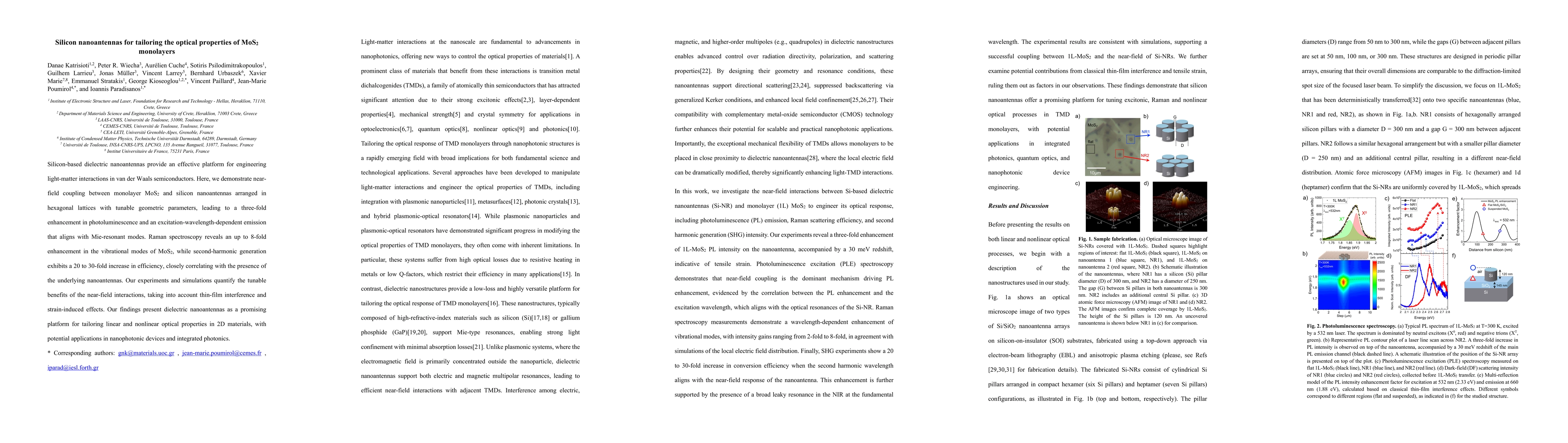
Silicon-based dielectric nanoantennas provide an effective platform for engineering light-matter interactions in van der Waals semiconductors. Here, we demonstrate near-field coupling between monolaye...
The van der Waals antiferromagnet CrSBr exhibits coupling of vibrational, electronic, and magnetic degrees of freedom, giving rise to distinctive quasi-particle interactions. We investigate these inte...
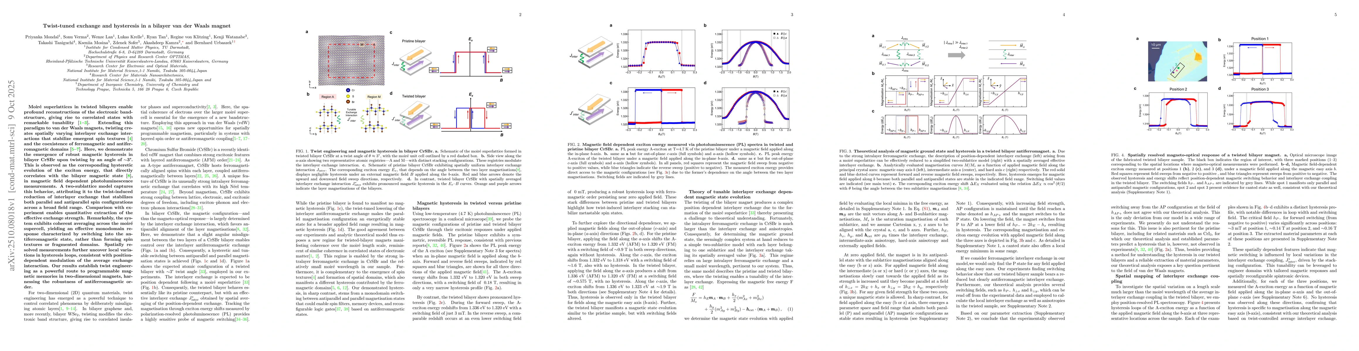
Moir\'e superlattices in twisted bilayers enable profound reconstructions of the electronic bandstructure, giving rise to correlated states with remarkable tunability. Extending this paradigm to van d...
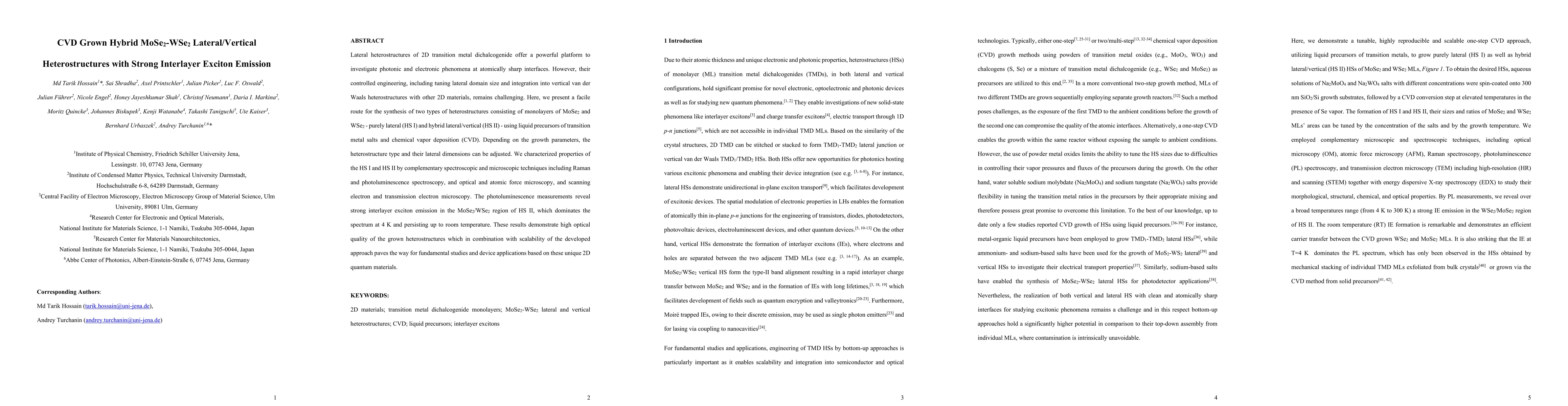
Lateral heterostructures of 2D transition metal dichalcogenide offer a powerful platform to investigate photonic and electronic phenomena at atomically sharp interfaces. However, their controlled engi...
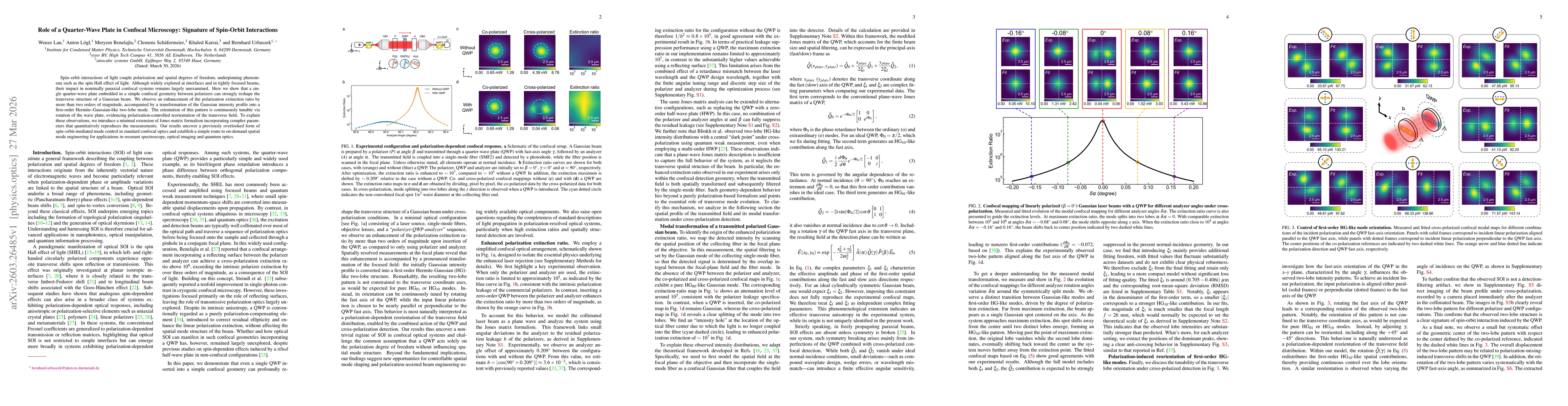
Spin-orbit interactions of light couple polarization and spatial degrees of freedom, underpinning phenomena such as the spin Hall effect of light. Although widely explored at interfaces and in tightly...