Academic Profile
Statistics
Similar Authors
Papers on arXiv
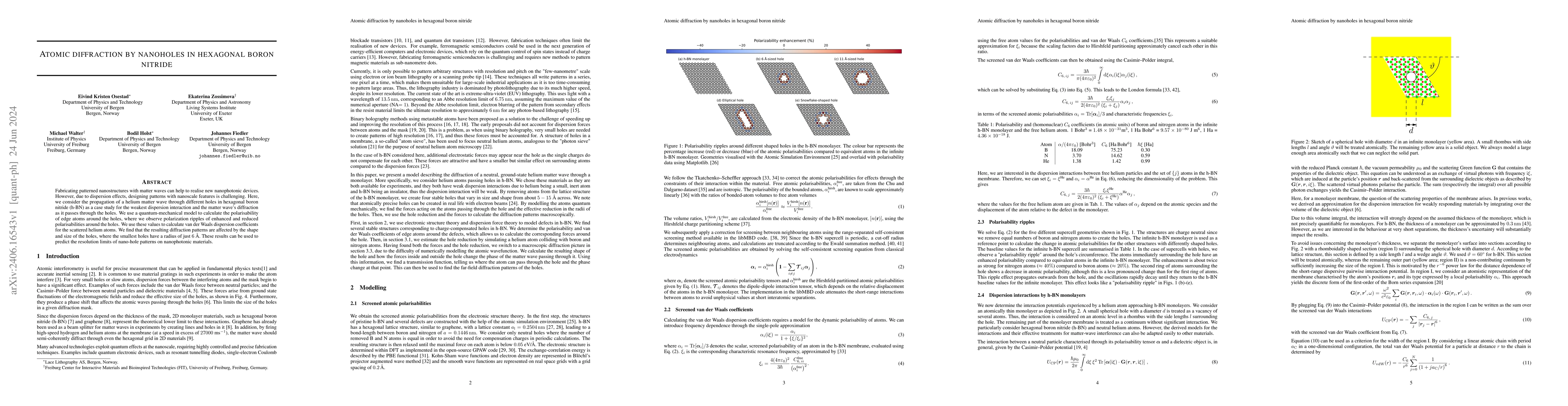
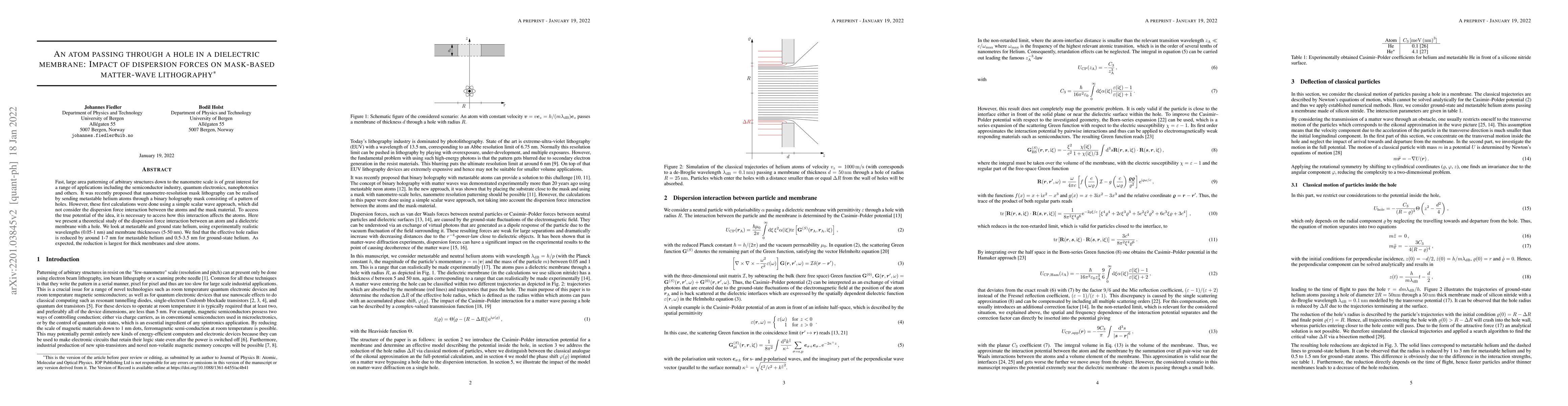
Fabricating patterned nanostructures with matter waves can help to realise new nanophotonic devices. However, due to dispersion effects, designing patterns with nanoscale features is challenging. He...
Atom and, of late, molecule interferometers find application in both the crucible of fundamental research and industrial pursuits. A prevalent methodology in the construction of atom interferometers...
This document presents a summary of the 2023 Terrestrial Very-Long-Baseline Atom Interferometry Workshop hosted by CERN. The workshop brought together experts from around the world to discuss the ex...
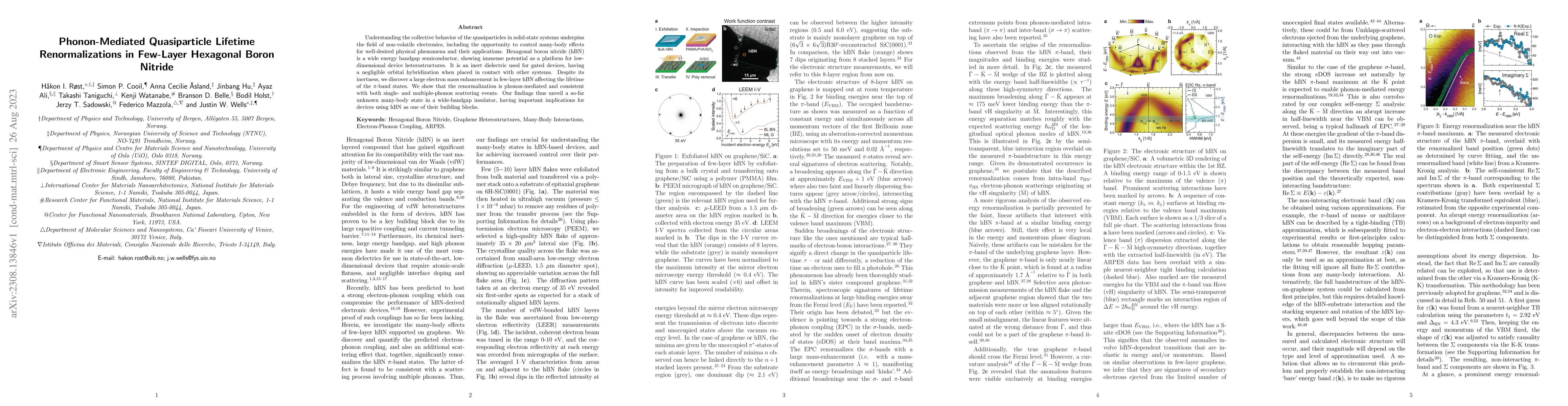
Understanding the collective behavior of the quasiparticles in solid-state systems underpins the field of non-volatile electronics, including the opportunity to control many-body effects for well-de...
Neutral helium atom microscopy is a novel microscopy technique that offers strictly surface-sensitive, non-destructive imaging. Several experiments have been published in recent years where images a...
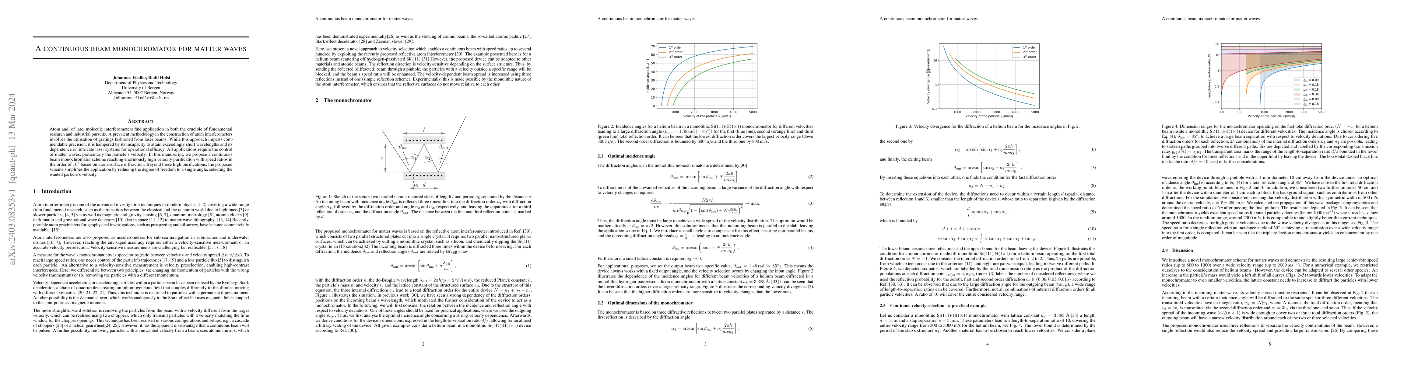
Atom and, more recently, molecule interferometers are used in fundamental research and industrial applications. Most atom interferometers rely on gratings made from laser beams, which can provide hi...
In classical binary holography, a target pattern located at infinity is generated by the diffraction of a plane wave passing through a binary mask with holes of the same size, placed at specific pos...
Fast production of large area patterns with nanometre resolution is crucial for the established semiconductor industry and for enabling industrial-scale production of next-generation quantum devices...
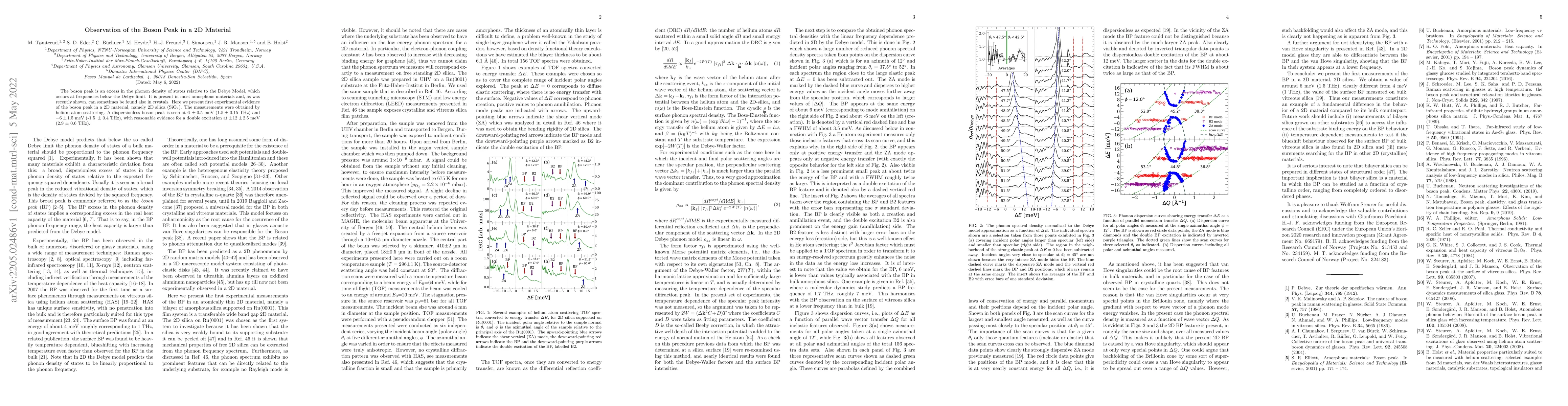
The boson peak is an excess in the phonon density of states relative to the Debye Model, which occurs at frequencies below the Debye limit. It is present in most amorphous materials and, as was rece...
We summarize the discussions at a virtual Community Workshop on Cold Atoms in Space concerning the status of cold atom technologies, the prospective scientific and societal opportunities offered by ...
Fast, large area patterning of arbitrary structures down to the nanometre scale is of great interest for a range of applications including the semiconductor industry, quantum electronics, nanophoton...
Neutral helium atom microscopy, also referred to as scanning helium microscopy and commonly abbreviated SHeM or NAM (neutral atom microscopy), is a novel imaging technique that uses a beam of neutra...
This summary of the second Terrestrial Very-Long-Baseline Atom Interferometry (TVLBAI) Workshop provides a comprehensive overview of our meeting held in London in April 2024, building on the initial d...