Academic Profile
Statistics
Similar Authors
Papers on arXiv
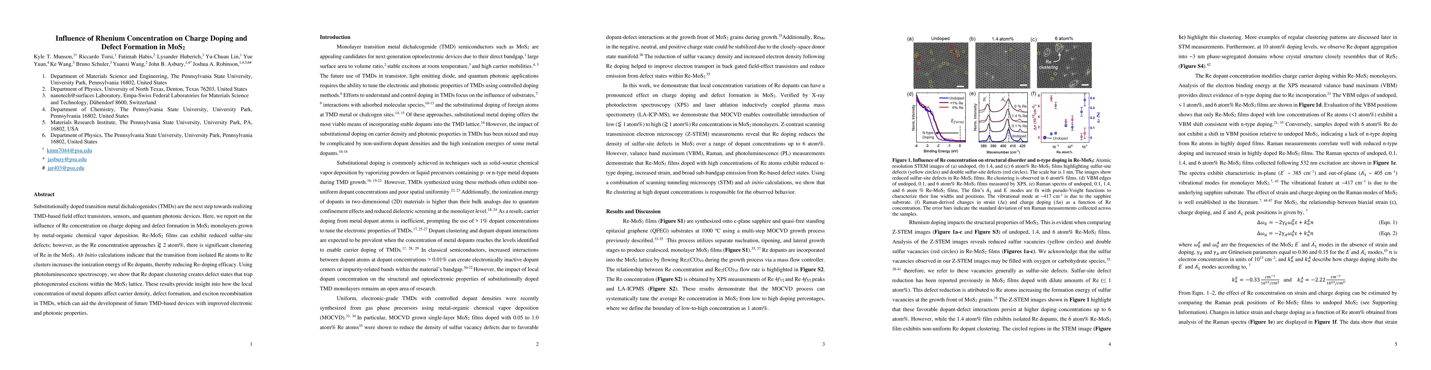
Substitutionally doped transition metal dichalcogenides (TMDs) are the next step towards realizing TMD-based field effect transistors, sensors, and quantum photonic devices. Here, we report on the i...
The functionality of atomic quantum emitters is intrinsically linked to their host lattice coordination. Structural distortions that spontaneously break the lattice symmetry strongly impact their op...
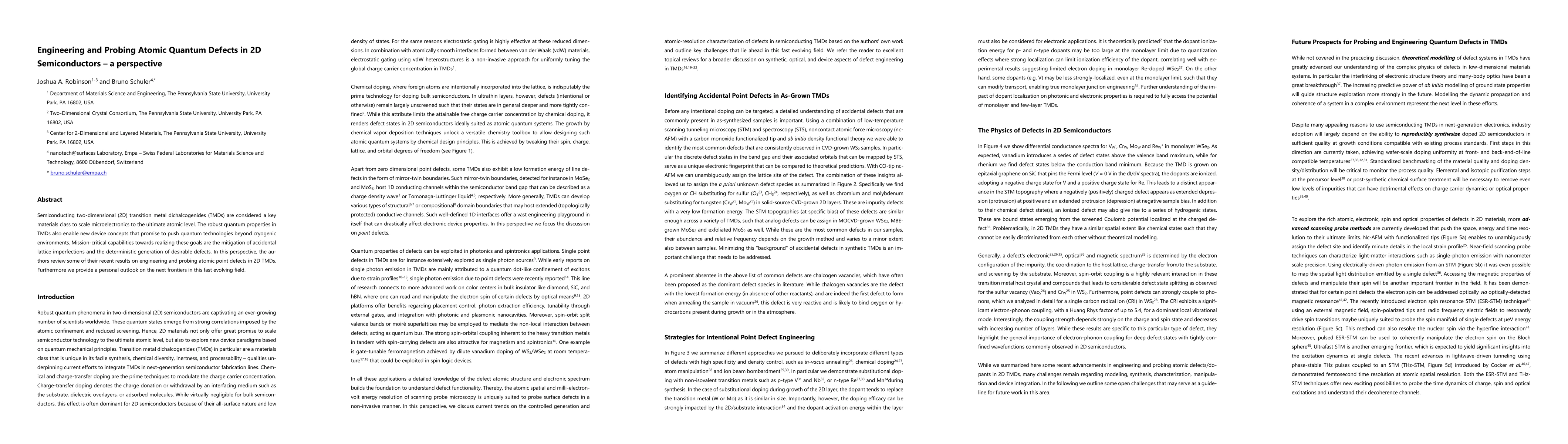
Substitutionally-doped 2D transition metal dichalcogenides are primed for next-generation device applications such as field effect transistors (FET), sensors, and optoelectronic circuits. In this wo...
Semiconducting two-dimensional (2D) transition metal dichalcogenides (TMDs) are considered a key materials class to scale microelectronics to the ultimate atomic level. The robust quantum properties...
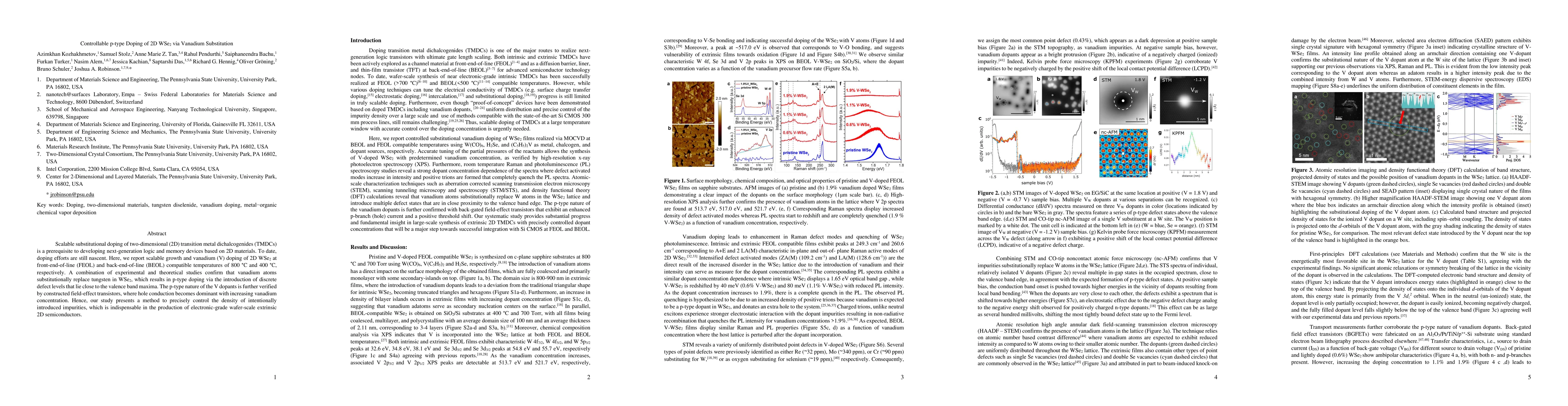
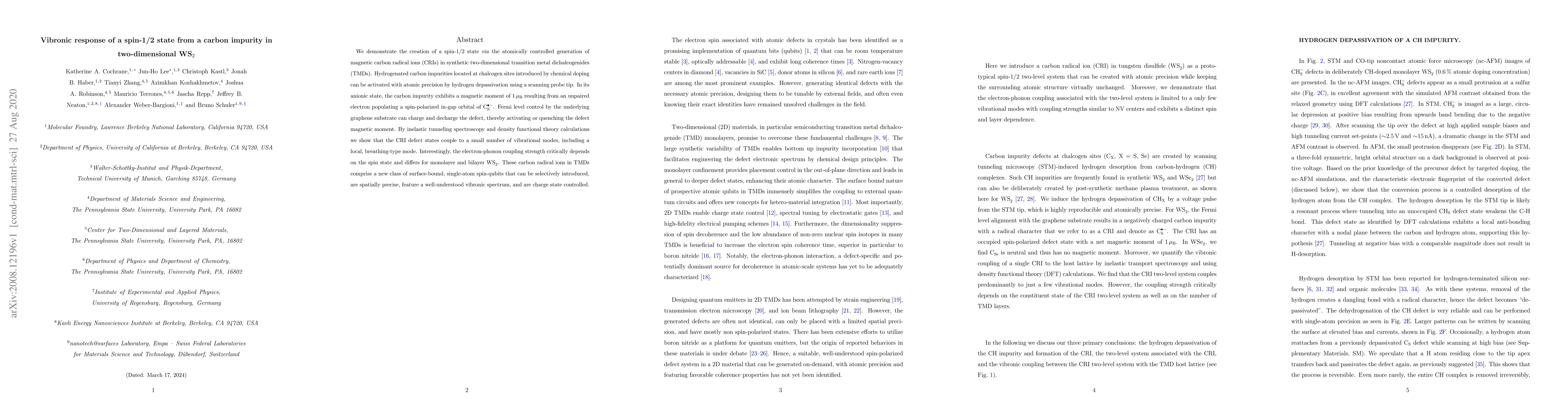
Scalable substitutional doping of two-dimensional (2D) transition metal dichalcogenides (TMDCs) is a prerequisite to developing next-generation logic and memory devices based on 2D materials. To dat...
We demonstrate the creation of a spin-1/2 state via the atomically controlled generation of magnetic carbon radical ions (CRIs) in synthetic two-dimensional transition metal dichalcogenides (TMDs). ...
Control of impurity concentrations in semiconducting materials is essential to device technology. Because of their intrinsic confinement, the properties of two-dimensional semiconductors such as tra...
Optical quantum emitters are a key component of quantum devices for metrology and information processing. In particular, atomic defects in 2D materials can operate as optical quantum emitters that o...
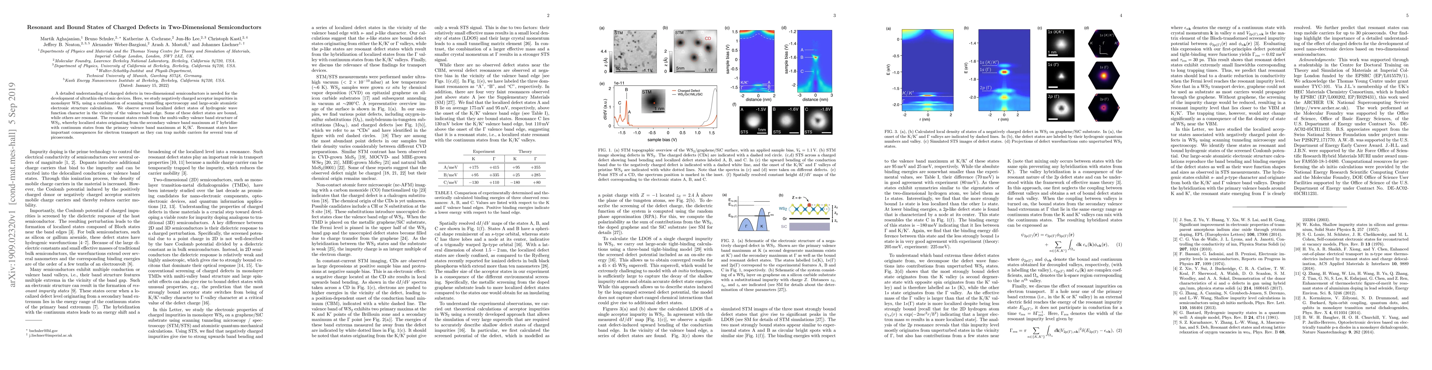
A detailed understanding of charged defects in two-dimensional semiconductors is needed for the development of ultrathin electronic devices. Here, we study negatively charged acceptor impurities in ...
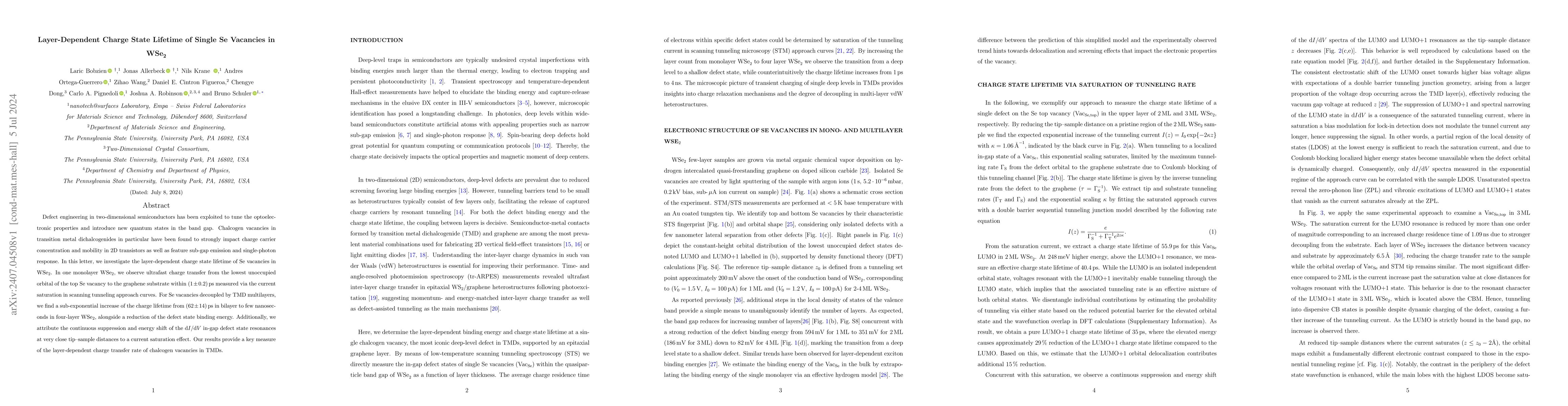
Defect engineering in two-dimensional semiconductors has been exploited to tune the optoelectronic properties and introduce new quantum states in the band gap. Chalcogen vacancies in transition metal ...
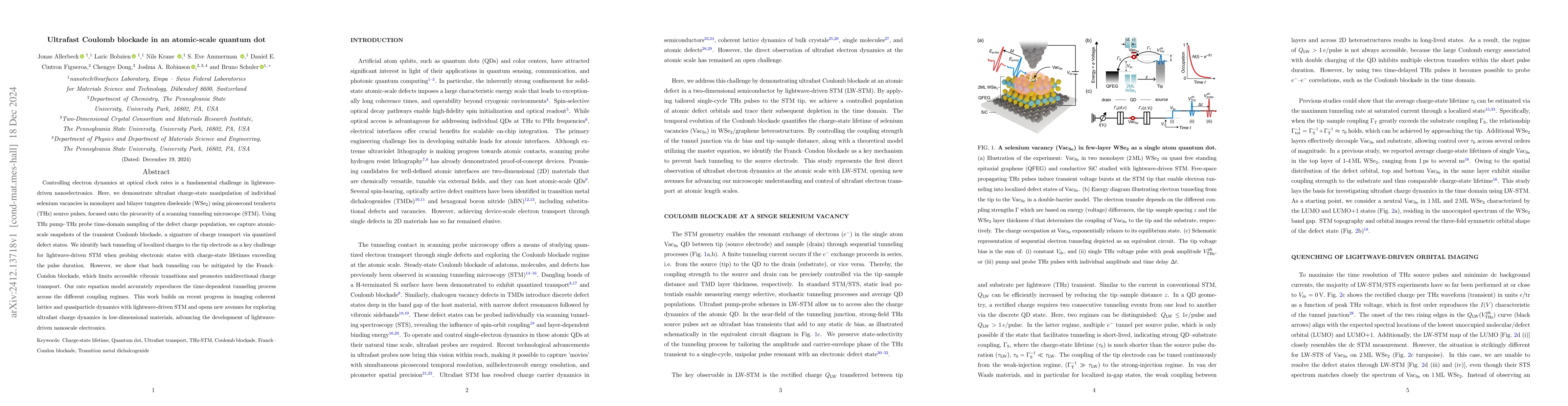
Controlling electron dynamics at optical clock rates is a fundamental challenge in lightwave-driven nanoelectronics. Here, we demonstrate ultrafast charge-state manipulation of individual selenium vac...
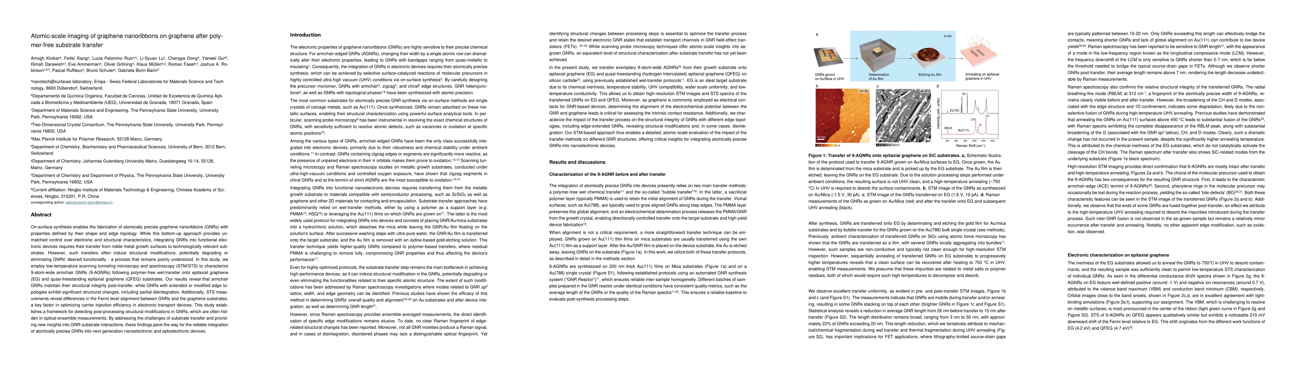
On-surface synthesis enables the fabrication of atomically precise graphene nanoribbons (GNRs) with properties defined by their shape and edge topology. While this bottom-up approach provides unmatche...
Understanding interfacial interactions in two-dimensional (2D) heterostructures is essential for advancing optoelectronic and quantum technologies. We investigate metal-organic chemical vapor depositi...
Understanding how atomic defects shape the nanoscale optical properties of two-dimensional (2D) semiconductors is essential for advancing quantum technologies and optoelectronics. Using scanning tunne...
Characterizing the electronic properties of single atoms, molecules, and nanostructures is the hallmark of scanning tunneling microscopy (STM). Recently, exploration of a complex manifold of nonequili...