Academic Profile
Statistics
Similar Authors
Papers on arXiv
For the past few years, 2D ferroelectric materials have attracted strong interest for their potential in future nanoelectronics devices. The recent discovery of 2D ferroelectricity in twisted layers...
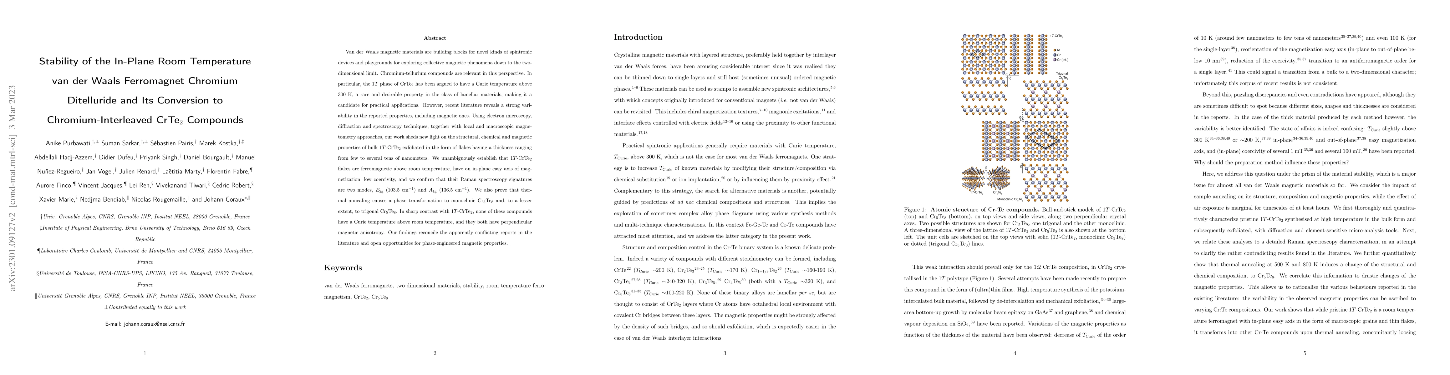
Van der Waals magnetic materials are building blocks for novel kinds of spintronic devices and playgrounds for exploring collective magnetic phenomena down to the two-dimensional limit. Chromium-tel...
We report one-pot chemical vapor deposition (CVD) growth of large-area Janus SeMoS monolayers, with the asymmetric top (Se) and bottom (S) chalcogen atomic planes with respect to the central transit...
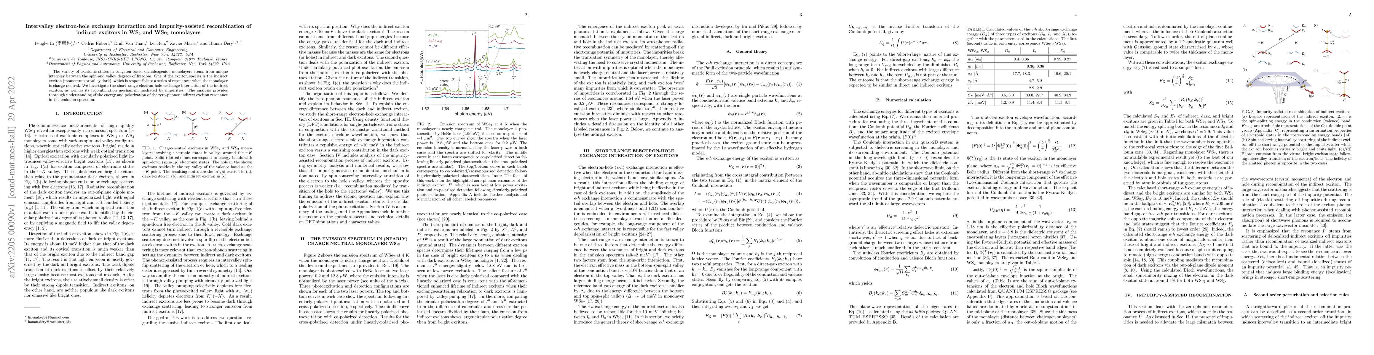
The variety of excitonic states in tungsten-based dichalcogenide monolayers stems from unique interplay between the spin and valley degrees of freedom. One of the exciton species is the indirect exc...
Using a spatially-resolved optical pump-probe experiment, we measure the lateral transport of spin/valley polarized electrons over very long distances (tens of micrometers) in a single WSe2 monolaye...
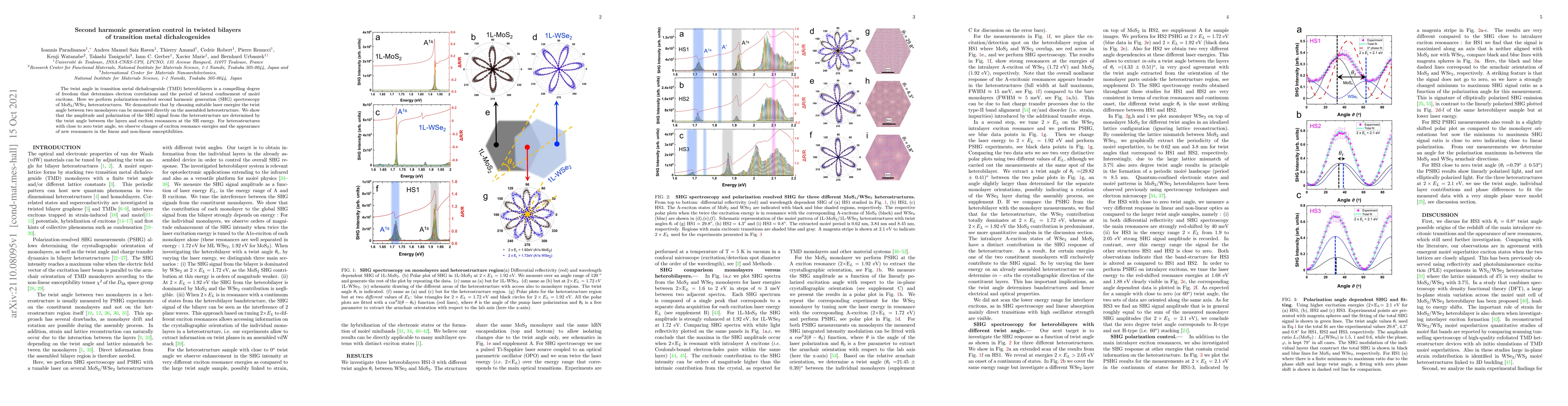
The twist angle in transition metal dichalcogenide (TMD) heterobilayers is a compelling degree of freedom that determines electron correlations and the period of lateral confinement of moir\'e excit...
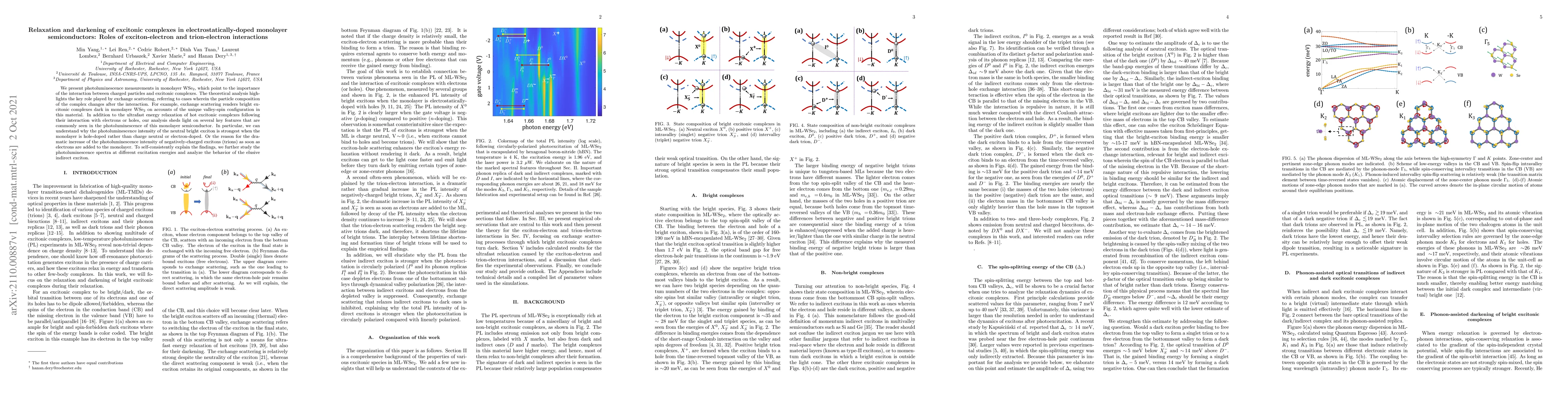
We present photoluminescence measurements in monolayer WSe$_2$, which point to the importance of the interaction between charged particles and excitonic complexes. The theoretical analysis highlight...
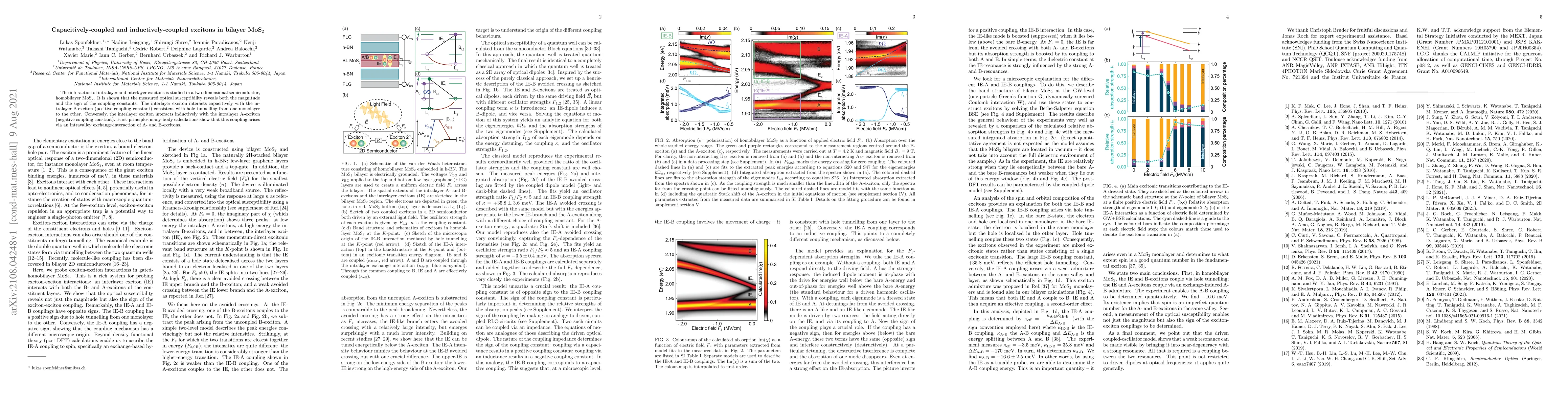
The interaction of intralayer and interlayer excitons is studied in a two-dimensional semiconductor, homobilayer MoS$_2$. It is shown that the measured optical susceptibility reveals both the magnit...
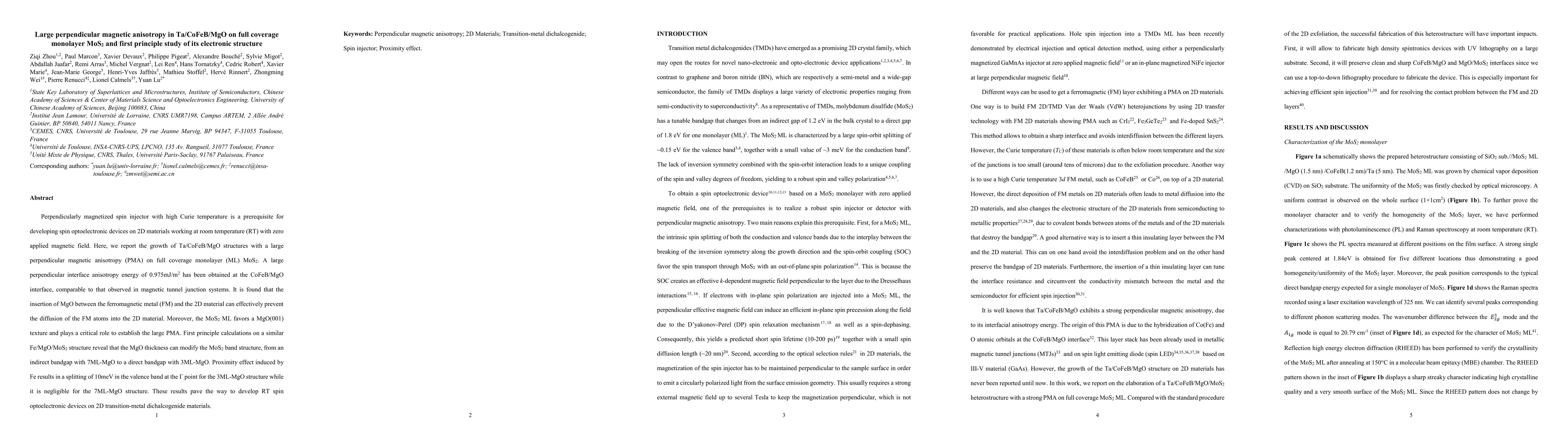
Perpendicularly magnetized spin injector with high Curie temperature is a prerequisite for developing spin optoelectronic devices on 2D materials working at room temperature (RT) with zero applied m...
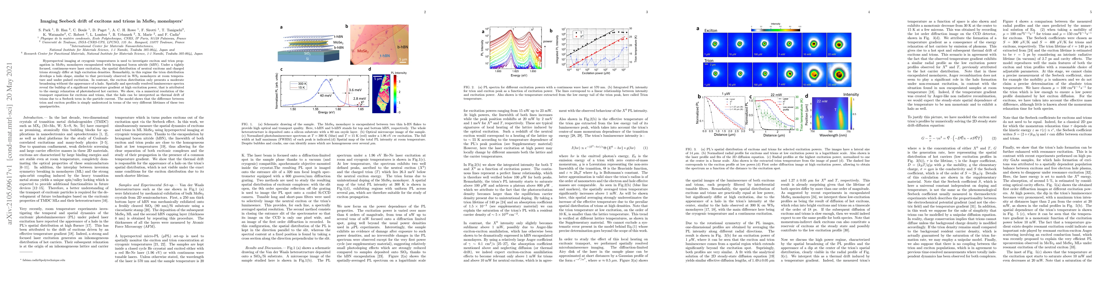
Hyperspectral imaging at cryogenic temperatures is used to investigate exciton and trion propagation in MoSe$_2$ monolayers encapsulated with hexagonal boron nitride (hBN). Under a tightly focused, ...
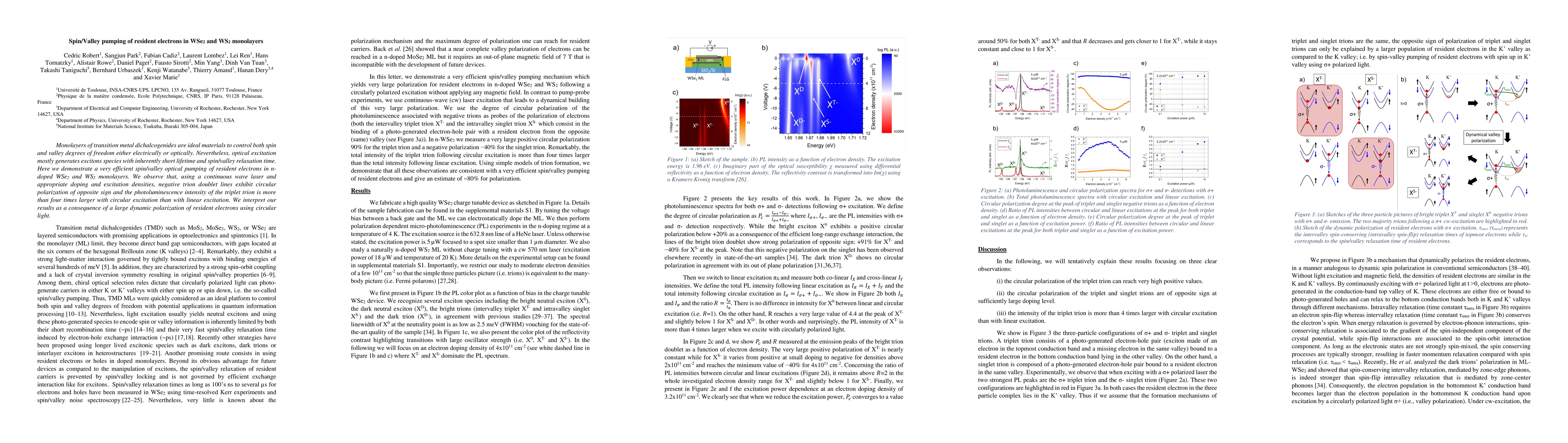
Monolayers of transition metal dichalcogenides are ideal materials to control both spin and valley degrees of freedom either electrically or optically. Nevertheless, optical excitation mostly genera...
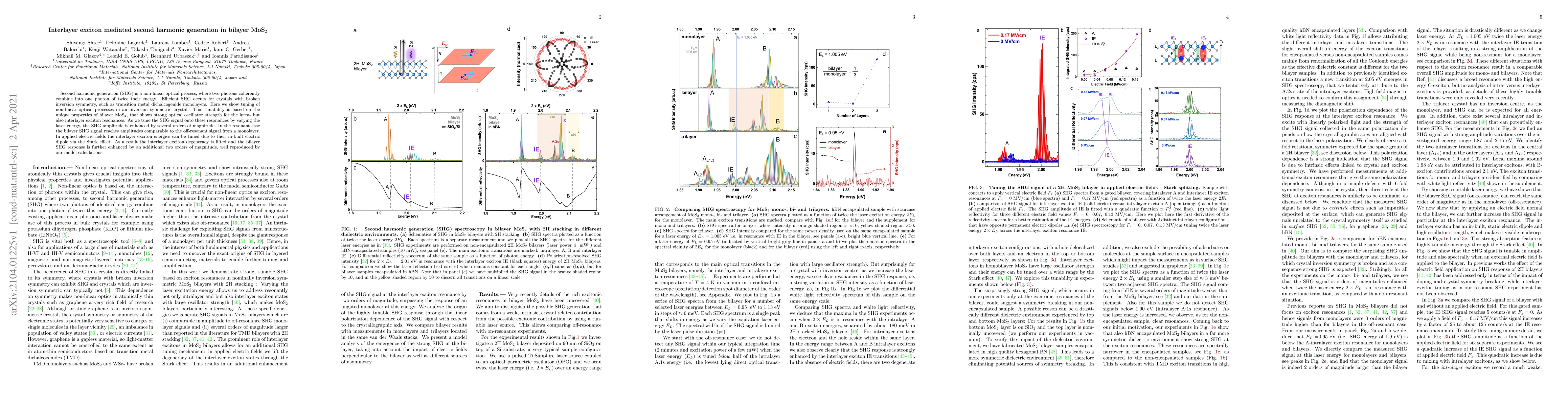
Second harmonic generation (SHG) is a non-linear optical process, where two photons coherently combine into one photon of twice their energy. Efficient SHG occurs for crystals with broken inversion ...
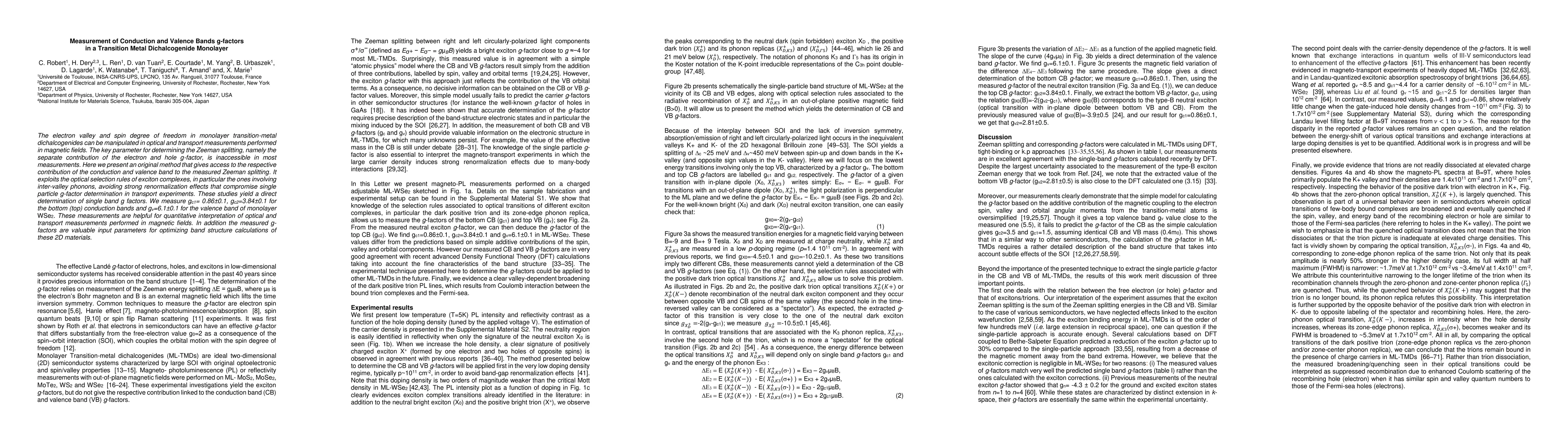
The electron valley and spin degree of freedom in monolayer transition-metal dichalcogenides can be manipulated in optical and transport measurements performed in magnetic fields. The key parameter ...
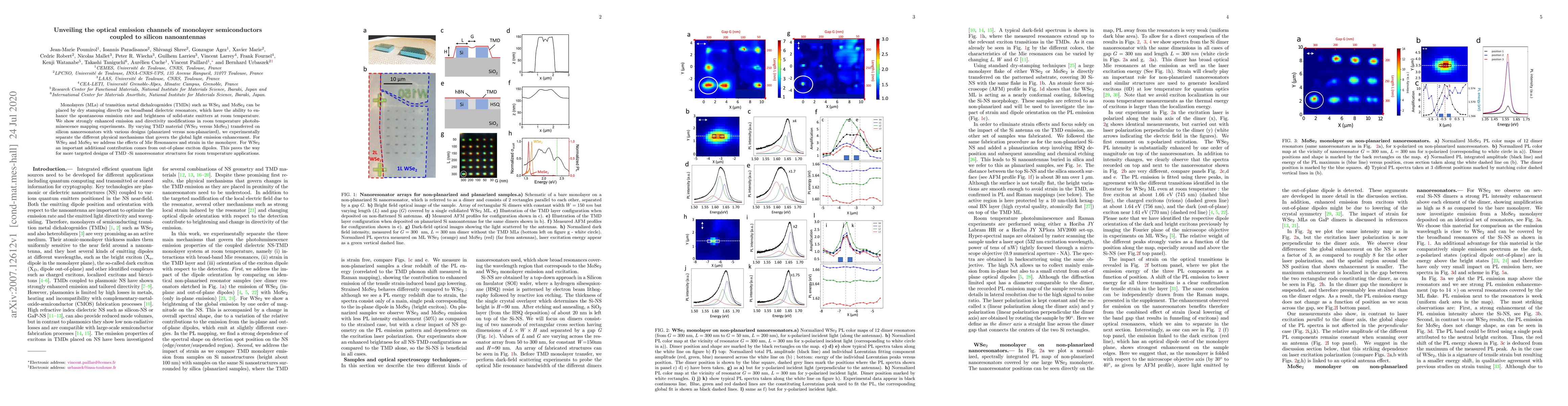
Monolayers (MLs) of transition metal dichalcogenides (TMDs) such as WSe2 and MoSe2 can be placed by dry stamping directly on broadband dielectric resonators, which have the ability to enhance the sp...
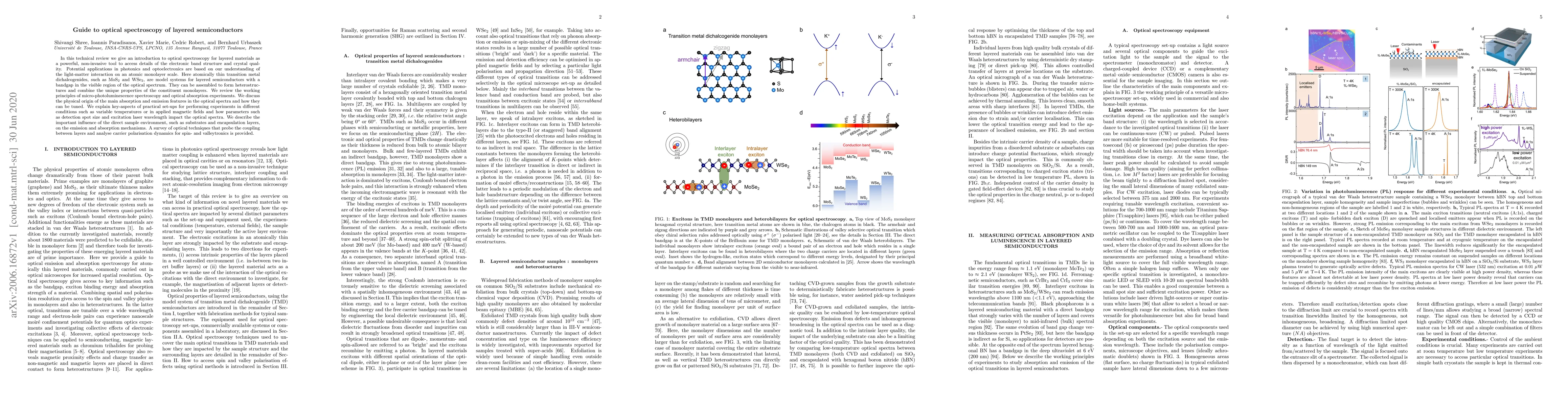
In this technical review we give an introduction to optical spectroscopy for layered materials as a powerful, non-invasive tool to access details of the electronic band structure and crystal quality...
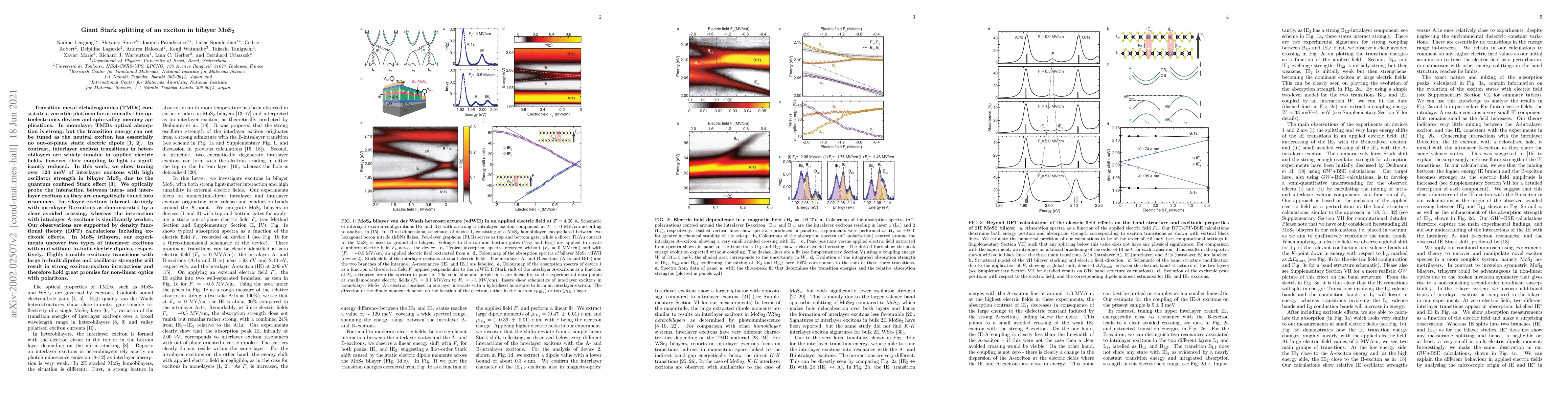
Transition metal dichalcogenides (TMDs) constitute a versatile platform for atomically thin optoelectronics devices and spin-valley memory applications. In monolayers optical absorption is strong, b...
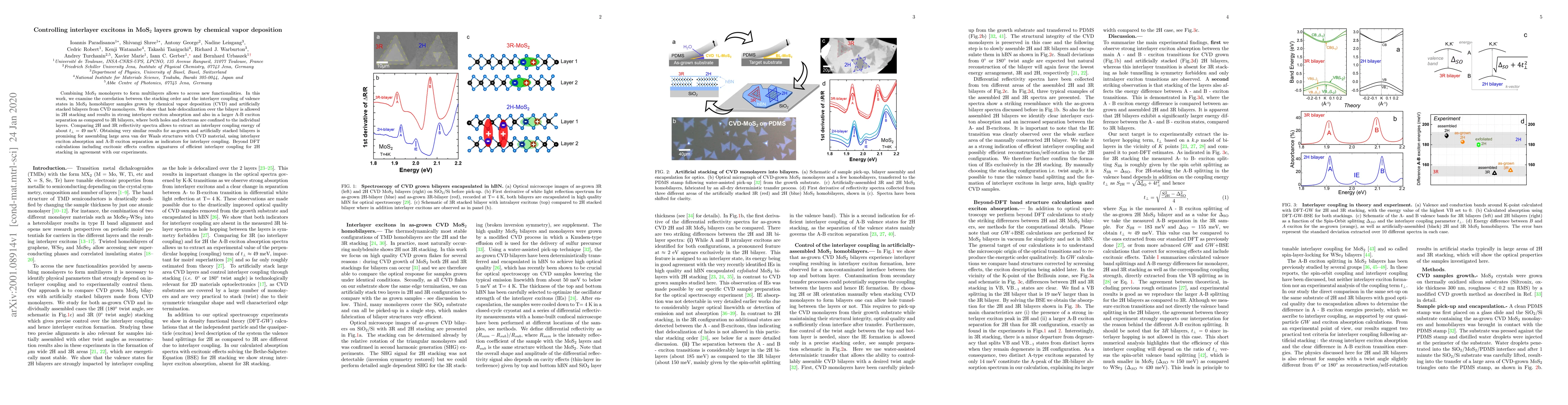
Combining MoS$_2$ monolayers to form multilayers allows to access new functionalities. In this work, we examine the correlation between the stacking order and the interlayer coupling of valence stat...
The valley degree of freedom is a sought-after quantum number in monolayer transition-metal dichalcogenides. Similar to optical spin orientation in semiconductors, the helicity of absorbed photons c...
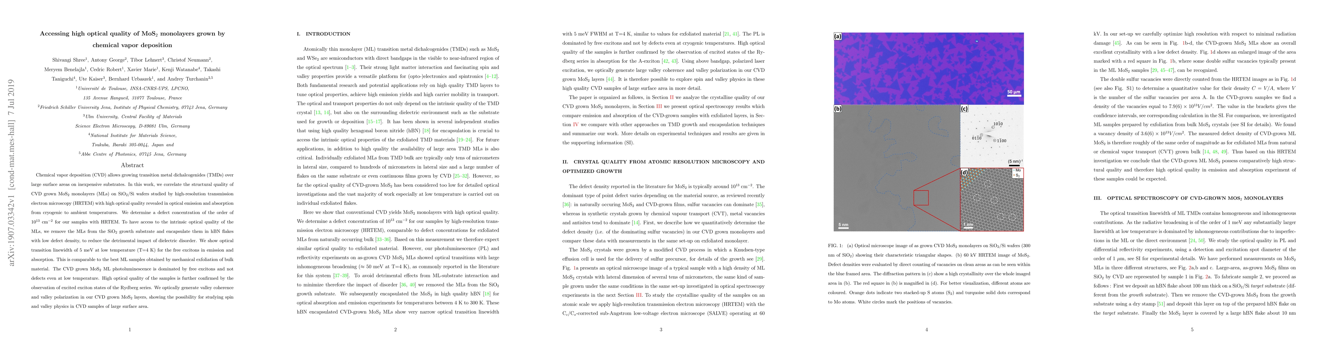
Chemical vapor deposition (CVD) allows growing transition metal dichalcogenides (TMDs) over large surface areas on inexpensive substrates. In this work, we correlate the structural quality of CVD gr...
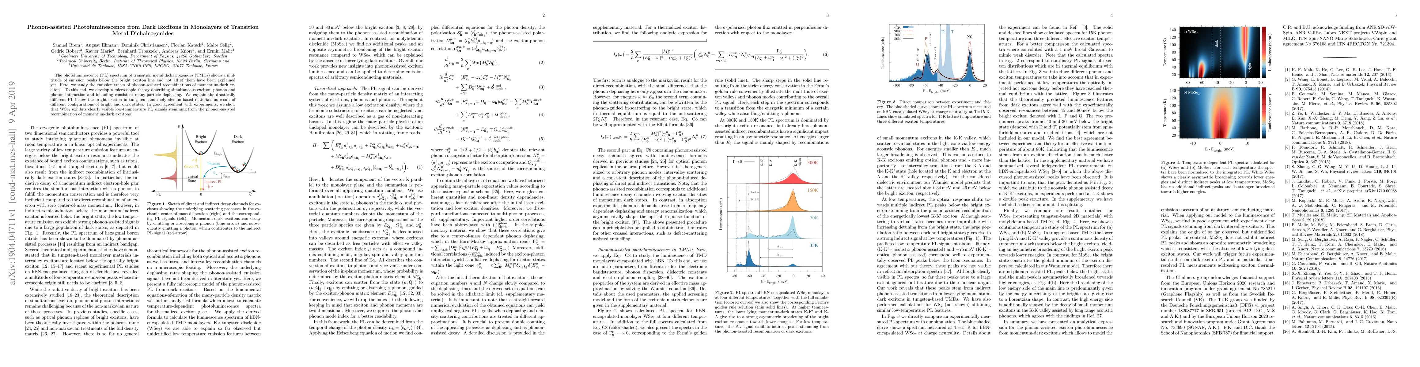
The photoluminescence (PL) spectrum of transition metal dichalcogenides (TMDs) shows a multitude of emission peaks below the bright exciton line and not all of them have been explained yet. Here, we...
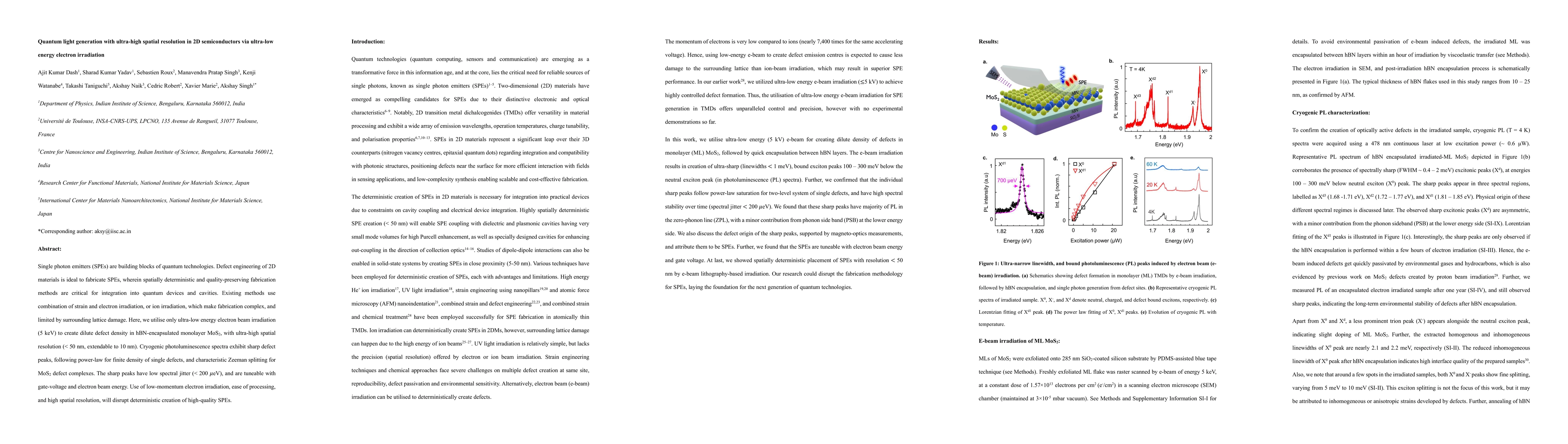
Single photon emitters (SPEs) are building blocks of quantum technologies. Defect engineering of 2D materials is ideal to fabricate SPEs, wherein spatially deterministic and quality-preserving fabrica...
Tuning the density of resident electrons or holes in semiconductors provides crucial insight into the composition of excitonic complexes that are observed as absorption or photoluminescence resonances...
Despite decades of research, demonstration of all-optical detection and control of free electron spins in silicon remains elusive. Here, we directly probe the electron spin properties in bulk silicon ...
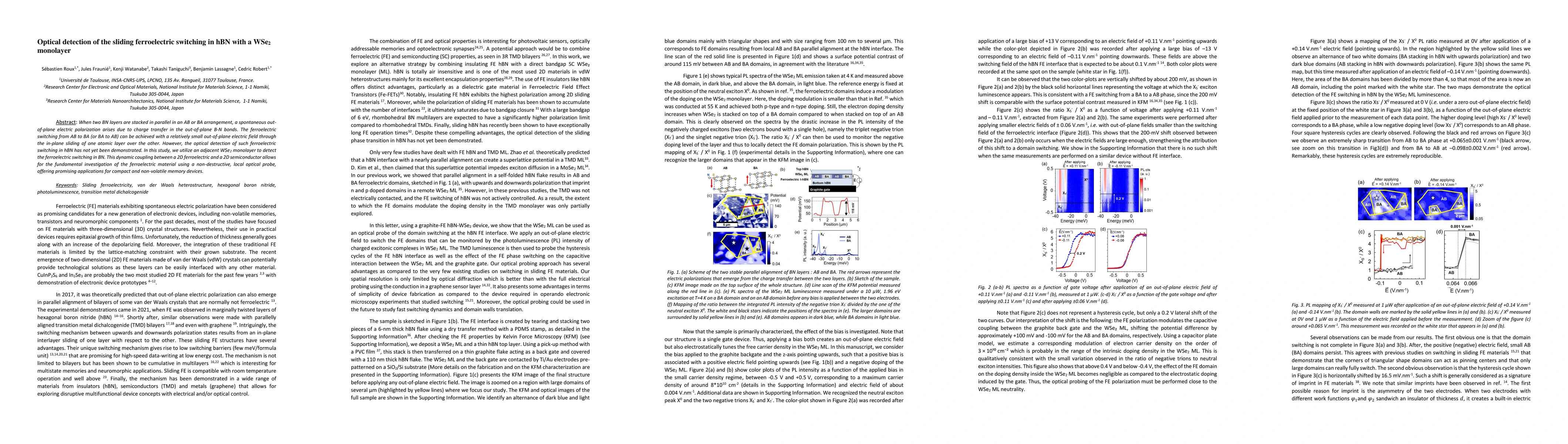
When two BN layers are stacked in parallel in an AB or BA arrangement, a spontaneous out-of-plane electric polarization arises due to charge transfer in the out-of-plane B-N bonds. The ferroelectric s...
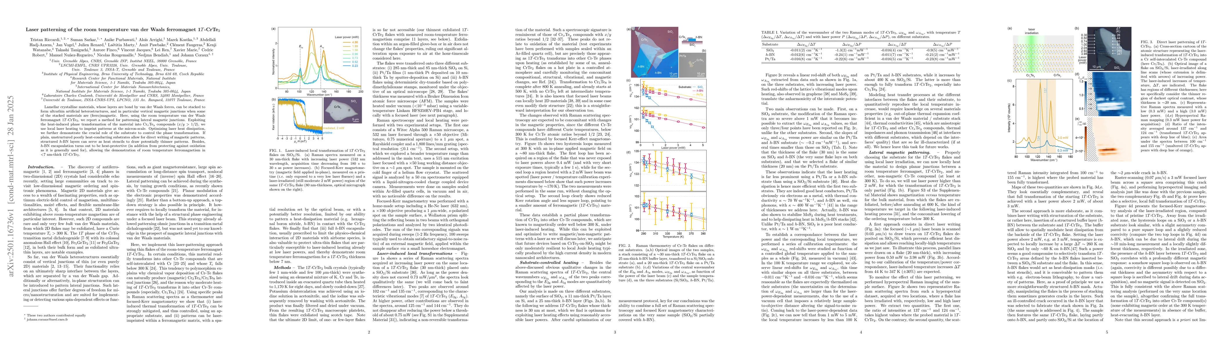
Lamellar crystalline materials, whose layers are bond by van der Waals forces, can be stacked to form ultrathin artificial heterostructures, and in particular vertical magnetic junctions when some of ...
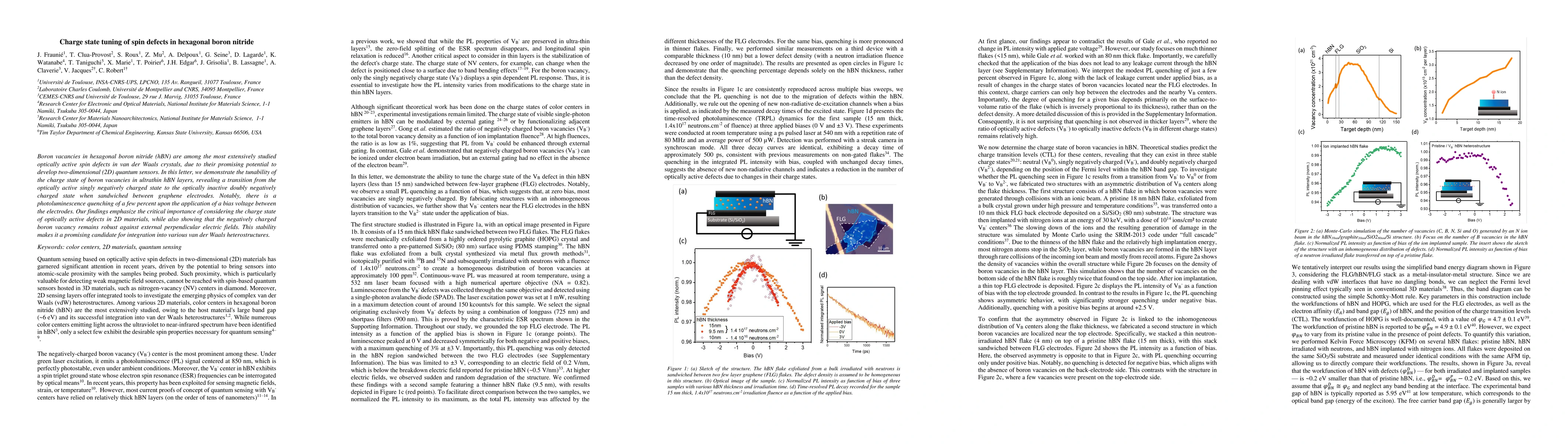
Boron vacancies in hexagonal boron nitride (hBN) are among the most extensively studied optically active spin defects in van der Waals crystals, due to their promising potential to develop two-dimensi...
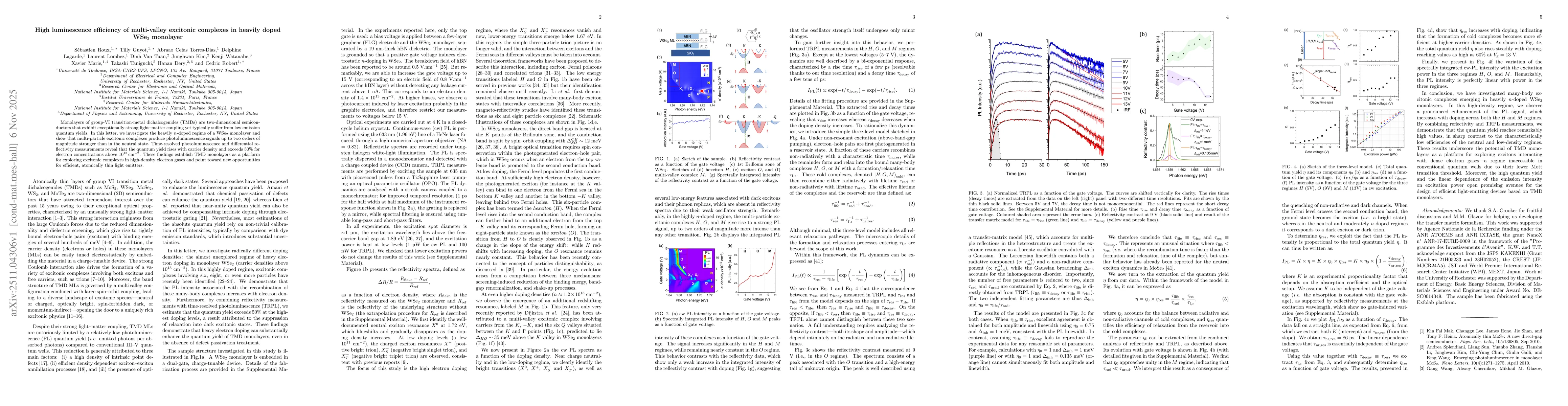
Monolayers of group-VI transition-metal dichalcogenides (TMDs) are two-dimensional semiconductors that exhibit exceptionally strong light-matter coupling yet typically suffer from low emission quantum...
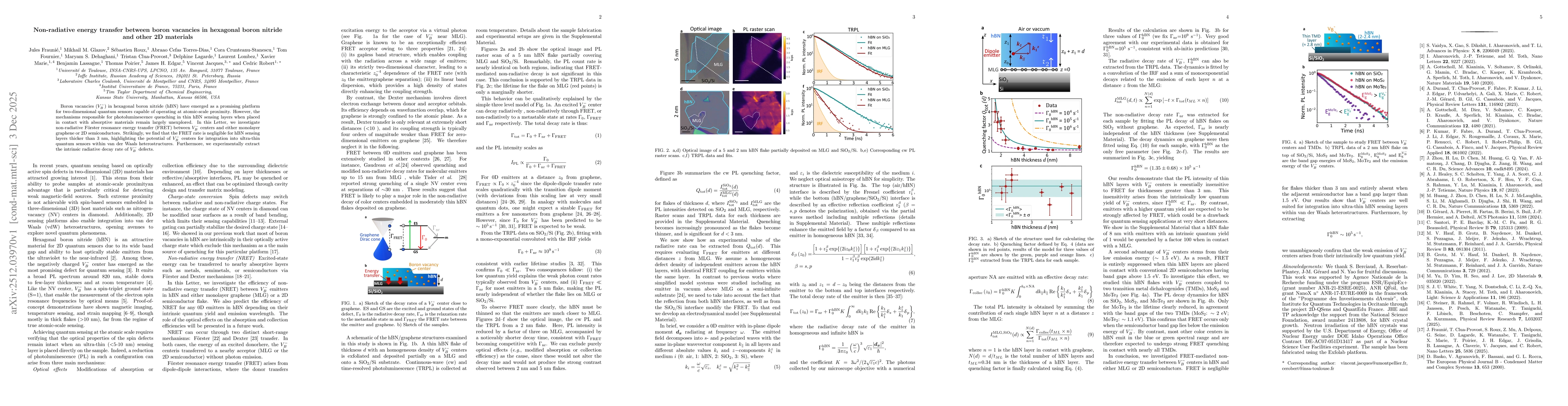
Boron vacancies ($V_B^-$) in hexagonal boron nitride (hBN) have emerged as a promising platform for two-dimensional quantum sensors capable of operating at atomic-scale proximity. However, the mechani...
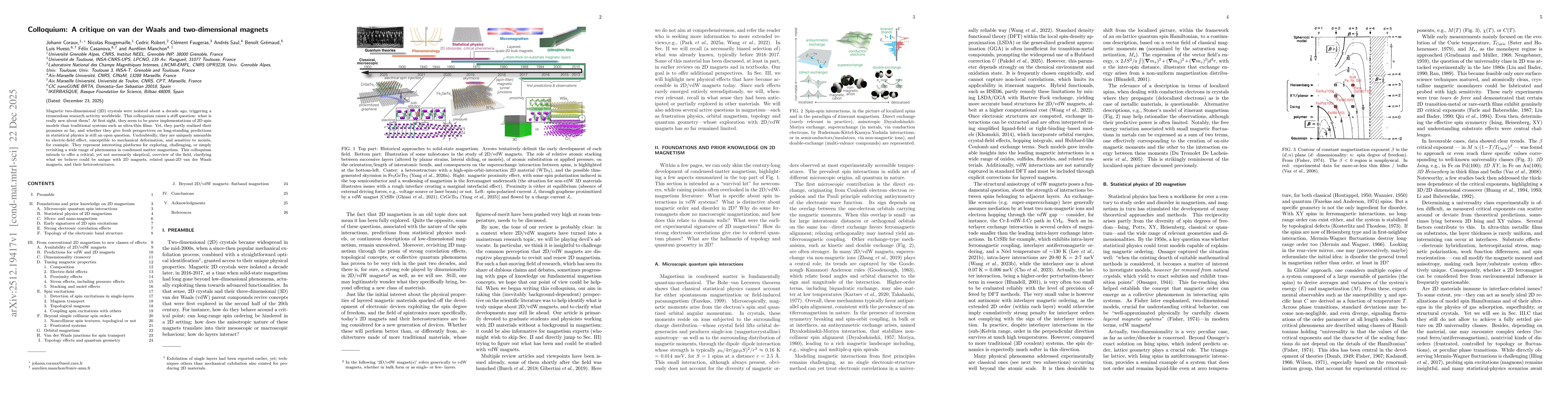
Magnetic two-dimensional (2D) crystals were isolated about a decade ago, triggering a tremendous research activity worldwide. This colloquium raises a stiff question: what is really new about them? At...
Single-photon emitters (SPEs) hosted by two-dimensional (2D) semiconducting materials are envisioned for next-generation quantum applications. However, SPE creation in 2D semiconductors on rigid subst...