ArxivLens
C
Researcher

Chandan Joishi

13 papers on arXiv

13 arXiv Papers
56 Total Publications
Profile

Academic Profile

Name C. Joishi
Total Papers 56
Scholar Profile View on Semantic Scholar
Metrics

Statistics

13 arXiv Papers
56 Total Publications
Publications

Papers on arXiv

Thumbnail for Tunnel Junction-Enabled Monolithically Integrated GaN Micro-Light
  Emitting Transistor
arXiv
Tunnel Junction-Enabled Monolithically Integrated GaN Micro-Light Emitting Transistor

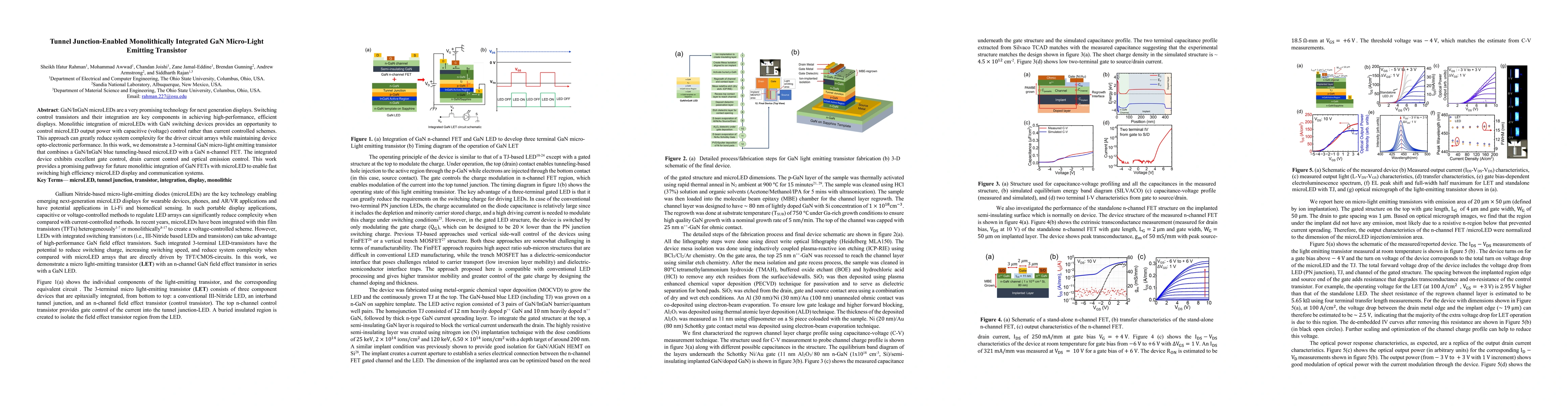
GaN/InGaN microLEDs are a very promising technology for next generation displays. Switching control transistors and their integration are key components in achieving high-performance, efficient disp...

Thumbnail for Design and Simulation of a III-Nitride Light Emitting Transistor
arXiv
Design and Simulation of a III-Nitride Light Emitting Transistor

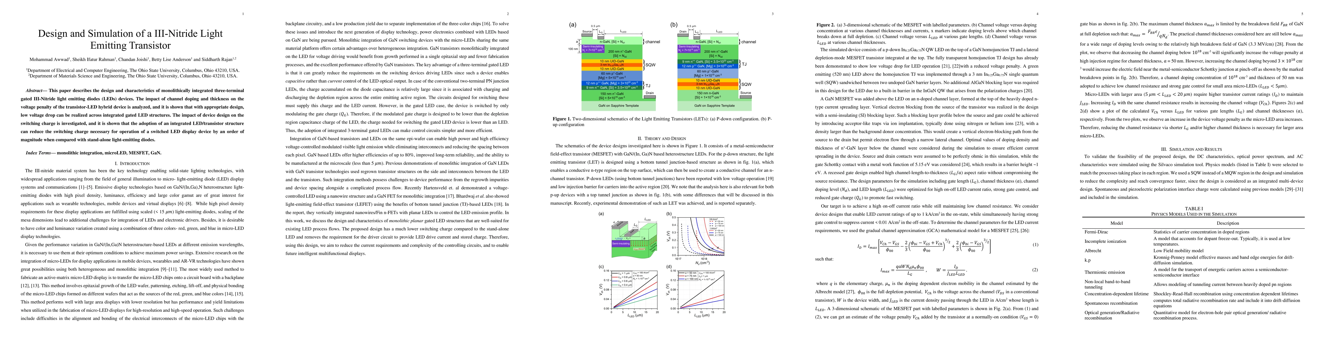
This paper describes the design and characteristics of monolithically integrated three-terminal gated III-Nitride light emitting diodes (LEDs) devices. The impact of channel doping and thickness on ...

Thumbnail for Selective injection AlGaN/GaN heterojunction bipolar transistors with
  patterned regrown base contacts
arXiv
Selective injection AlGaN/GaN heterojunction bipolar transistors with patterned regrown base contacts

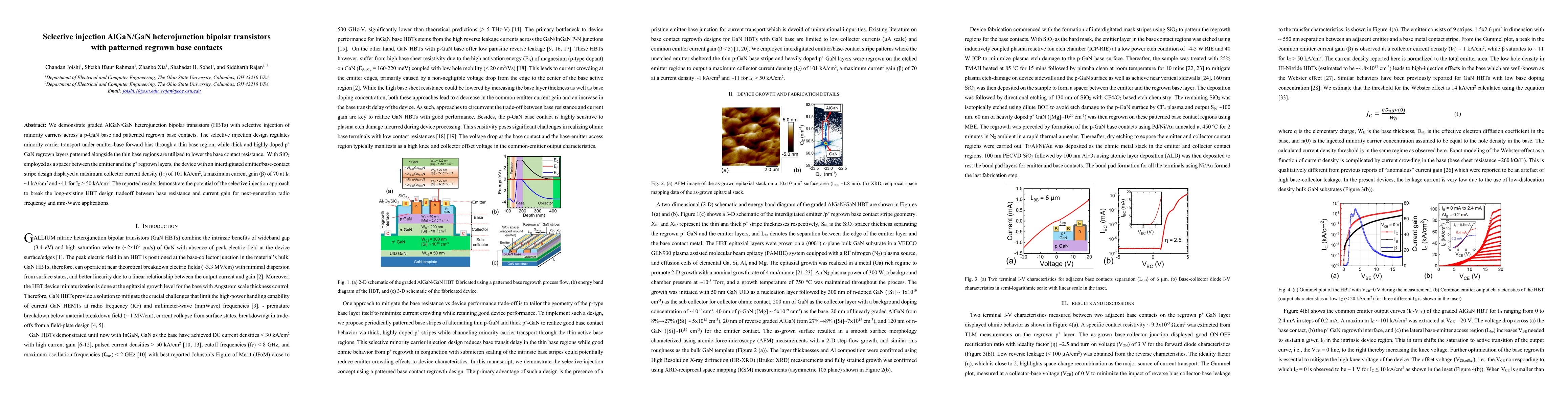
We demonstrate graded AlGaN/GaN heterojunction bipolar transistors (HBTs) with selective injection of minority carriers across a p-GaN base and patterned regrown base contacts. The selective injecti...

Thumbnail for $\beta$-Ga$_2$O$_3$ Trench Schottky Diodes by Novel Low-Damage Ga-Flux
  Etching
arXiv
$\beta$-Ga$_2$O$_3$ Trench Schottky Diodes by Novel Low-Damage Ga-Flux Etching

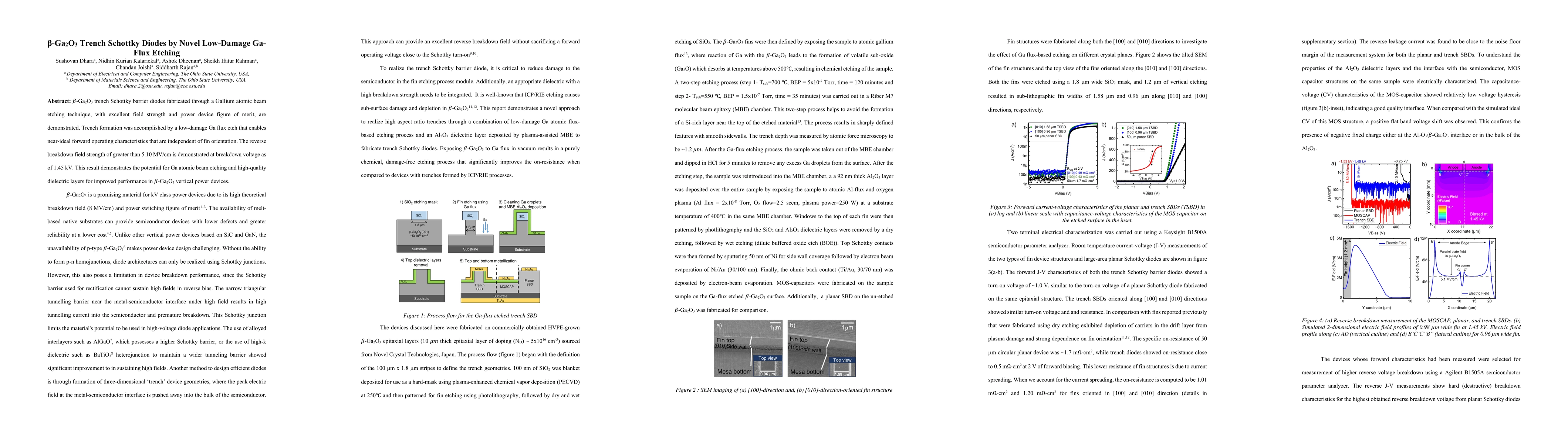
$\beta$-Ga$_2$O$_3$ trench Schottky barrier diodes fabricated through a Gallium atomic beam etching technique, with excellent field strength and power device figure of merit, are demonstrated. Trenc...

Thumbnail for Nb$_{2}$O$_{5}$ high-k dielectric enabled electric field engineering of
  $\beta$-Ga$_{2}$O$_{3}$ metal-insulator-semiconductor (MIS) diode
arXiv
Nb$_{2}$O$_{5}$ high-k dielectric enabled electric field engineering of $\beta$-Ga$_{2}$O$_{3}$ metal-insulator-semiconductor (MIS) diode

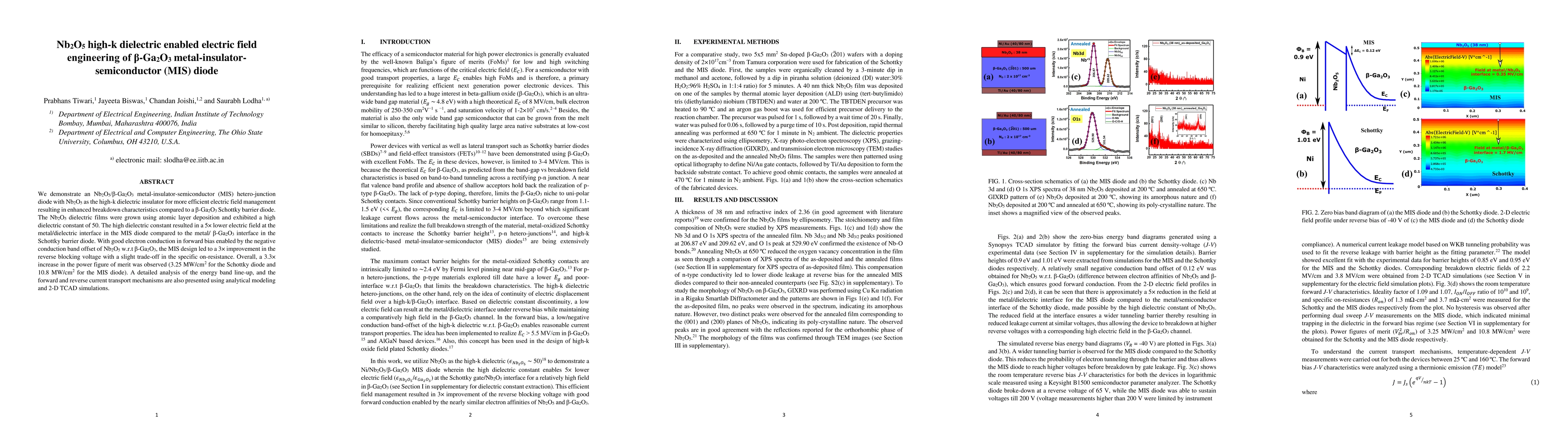
We demonstrate an Nb$_{2}$O$_{5}$/$\beta$-Ga$_{2}$O$_{3}$ metal-insulator-semiconductor (MIS) hetero-junction diode with Nb$_{2}$O$_{5}$ as the high-k dielectric insulator for more efficient electri...

Thumbnail for Charge trap layer enabled positive tunable V$_{fb}$ in
  $\beta$-Ga$_{2}$O$_{3}$ gate stacks for enhancement mode transistors
arXiv
Charge trap layer enabled positive tunable V$_{fb}$ in $\beta$-Ga$_{2}$O$_{3}$ gate stacks for enhancement mode transistors

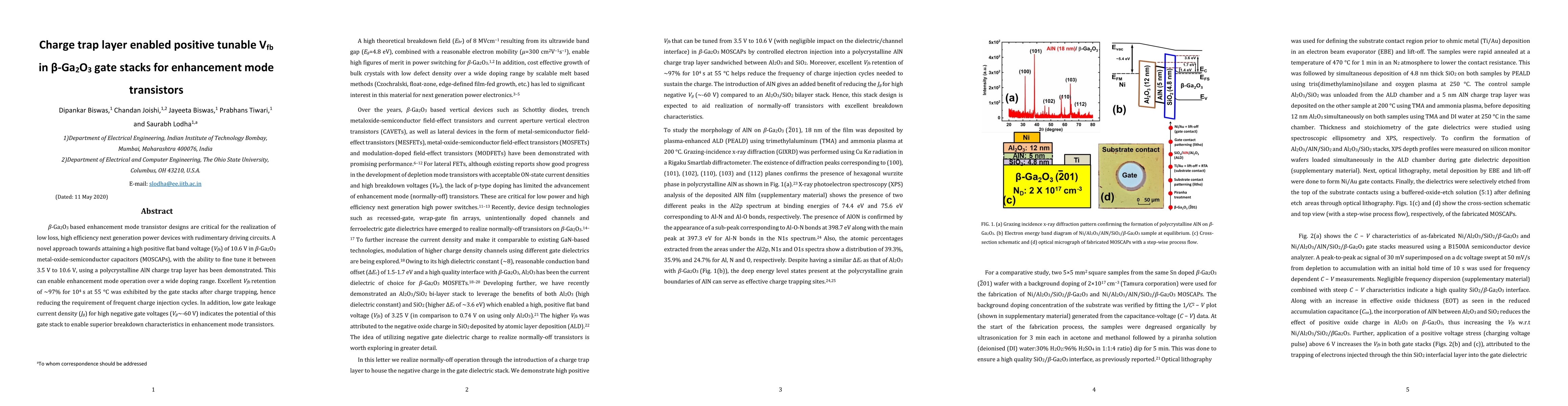
$\beta$-Ga$_{2}$O$_{3}$ based enhancement mode transistor designs are critical for the realization of low loss, high efficiency next generation power devices with rudimentary driving circuits. A nov...

Thumbnail for Deep-recessed $\beta$-Ga$_2$O$_3$ delta-doped field effect transistors
  with in situ epitaxial passivation
arXiv
Deep-recessed $\beta$-Ga$_2$O$_3$ delta-doped field effect transistors with in situ epitaxial passivation

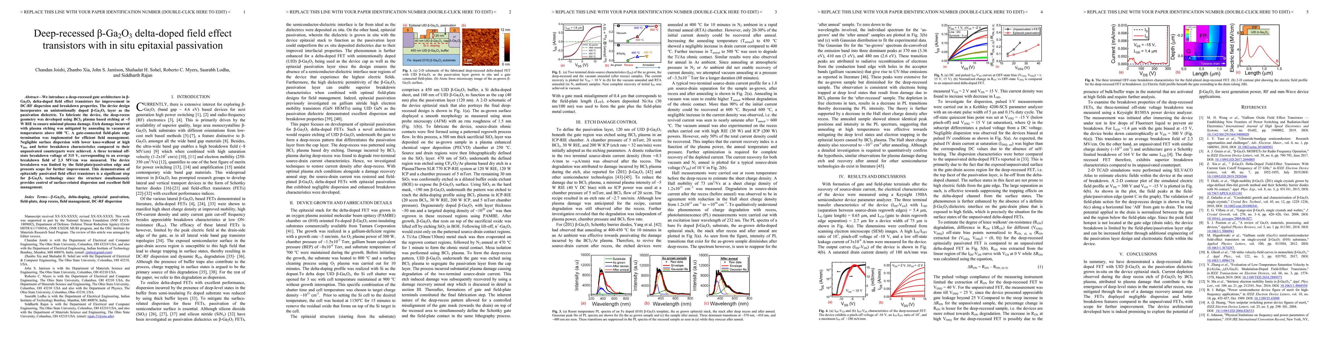
We introduce a deep-recessed gate architecture in $\beta$-Ga$_2$O$_3$ delta-doped field effect transistors for improvement in DC-RF dispersion and breakdown properties. The device design incorporate...

Thumbnail for Heterostructure and Interfacial Engineering for Low-Resistance Contacts
  to Ultra-Wide Bandgap AlGaN
arXiv
Heterostructure and Interfacial Engineering for Low-Resistance Contacts to Ultra-Wide Bandgap AlGaN

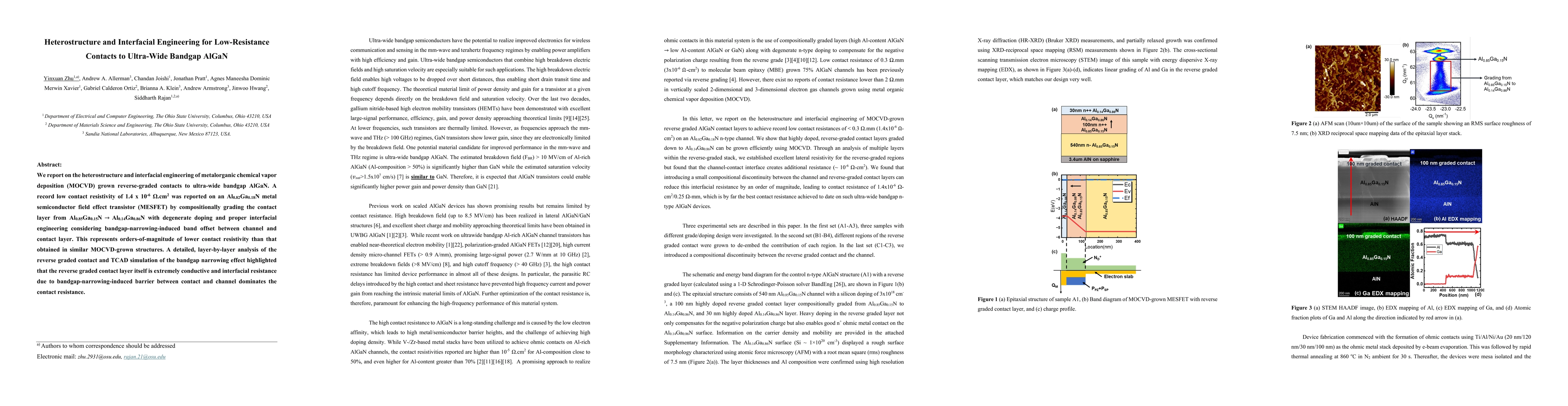
We report on the heterostructure and interfacial engineering of metalorganic chemical vapor deposition (MOCVD) grown reverse-graded contacts to ultra-wide bandgap AlGaN. A record low contact resistivi...

Thumbnail for Selective-injection GaN Heterojunction Bipolar Transistors with 275
  kA/cm$^2$ Current Density
arXiv
Selective-injection GaN Heterojunction Bipolar Transistors with 275 kA/cm$^2$ Current Density

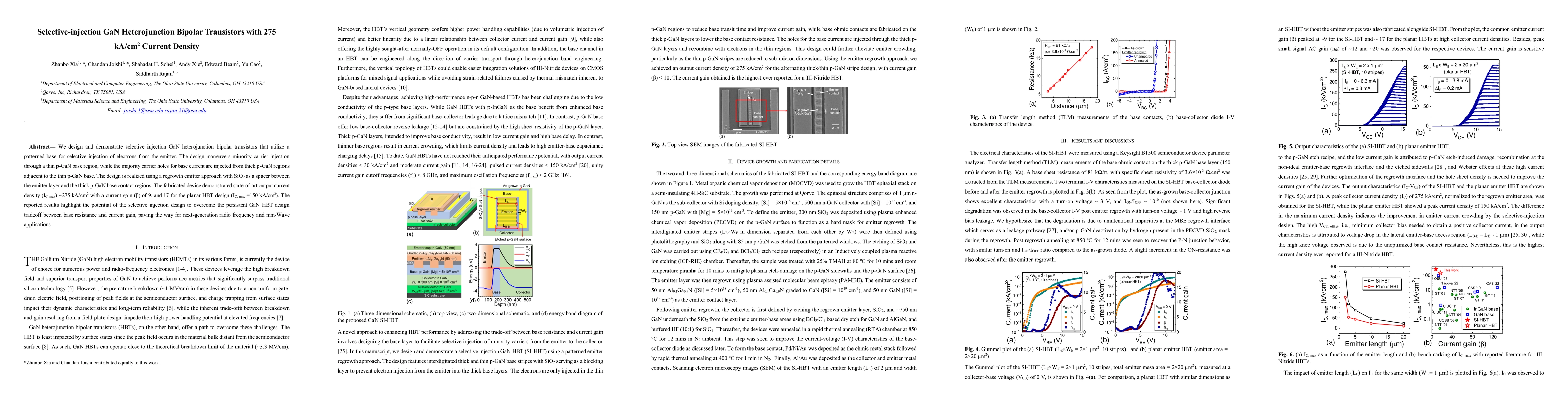
We design and demonstrate selective injection GaN heterojunction bipolar transistors that utilize a patterned base for selective injection of electrons from the emitter. The design maneuvers minority ...

Thumbnail for High Breakdown Electric Field (> 5 MV/cm) in UWBG AlGaN Transistors
arXiv
High Breakdown Electric Field (> 5 MV/cm) in UWBG AlGaN Transistors

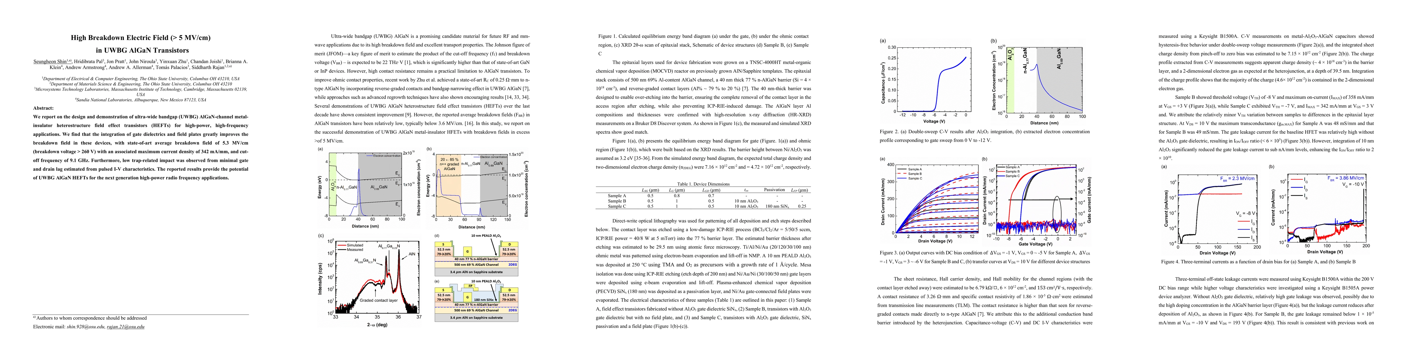
We report on the design and demonstration of ultra-wide bandgap (UWBG) AlGaN-channel metal-insulator heterostructure field effect transistors (HEFTs) for high-power, high-frequency applications. We fi...

Thumbnail for Energy Bands and Breakdown Characteristics in Al2O3/UWBG AlGaN
  Heterostructures
arXiv
Energy Bands and Breakdown Characteristics in Al2O3/UWBG AlGaN Heterostructures

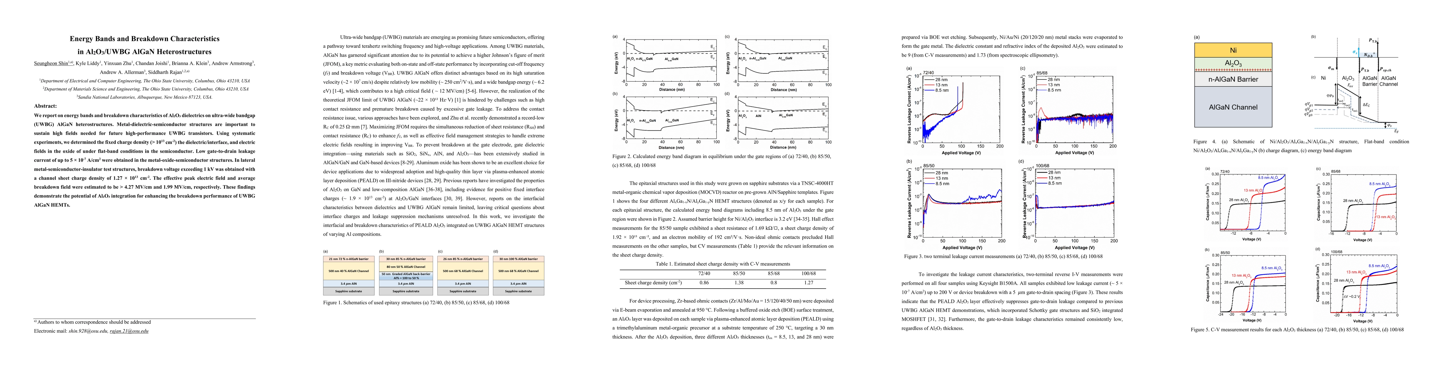
We report on energy bands and breakdown characteristics of Al2O3 dielectrics on ultra-wide bandgap (UWBG) AlGaN heterostructures. Metal-dielectric-semiconductor structures are important to sustain hig...

Thumbnail for Scaled Ultra-Wide Bandgap AlGaN Polarization-Graded FET with Ultra-thin Buffer Layer
arXiv
Scaled Ultra-Wide Bandgap AlGaN Polarization-Graded FET with Ultra-thin Buffer Layer

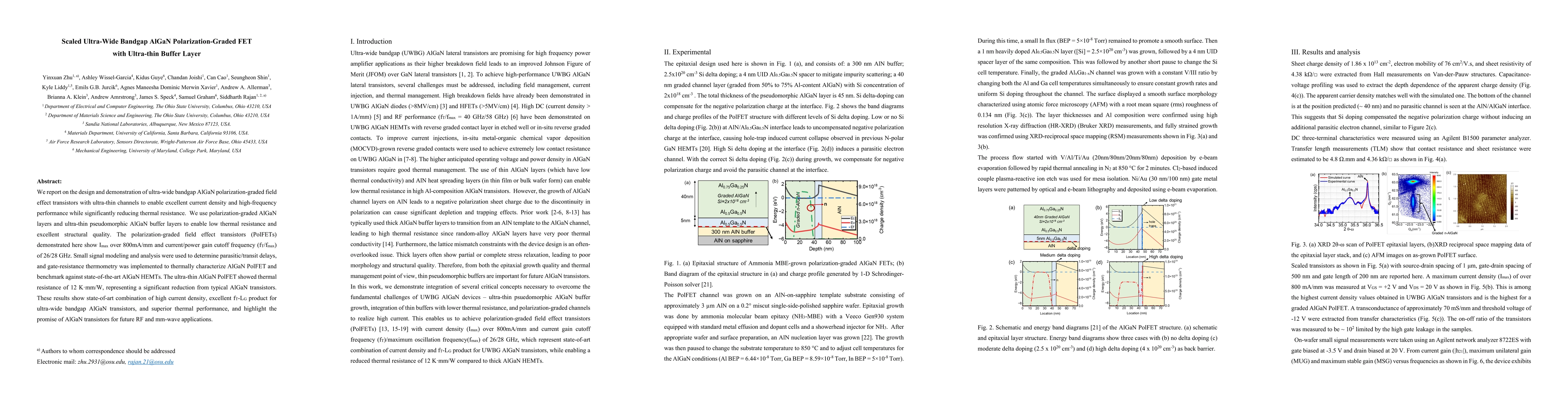
We report on the design and demonstration of ultra-wide bandgap AlGaN polarization-graded field effect transistors with ultra-thin channels to enable excellent current density and high-frequency perfo...

Thumbnail for A Promising Ohmic Contacts Approach for High-Al AlxGa1-xN (x>0.6) Channel HEMTs with AlN/GaN Digital Alloy Channel
arXiv
A Promising Ohmic Contacts Approach for High-Al AlxGa1-xN (x>0.6) Channel HEMTs with AlN/GaN Digital Alloy Channel

In this paper we report a novel ohmic contact formation scheme for Extreme Bandgap (EBG) AlxGa1-xN (x>0.6) channel HEMTs with undoped barrier layers. Our approach consists of using a new low temperatu...

This website uses cookies to ensure you get the best experience. Learn more