Academic Profile
Statistics
Similar Authors
Papers on arXiv
The crystallographic orientation of 3D materials grown over 2D material-covered substrates is one of the critical factors in discerning the true growth mechanism among competing possibilities, inclu...
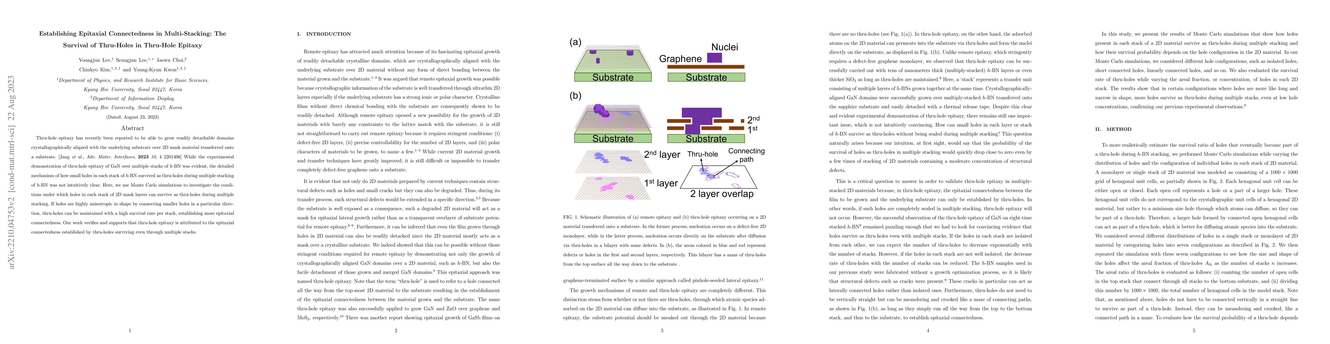
Thru-hole epitaxy has recently been reported to be able to grow readily detachable domains crystallographically aligned with the underlying substrate over 2D mask material transferred onto a substra...
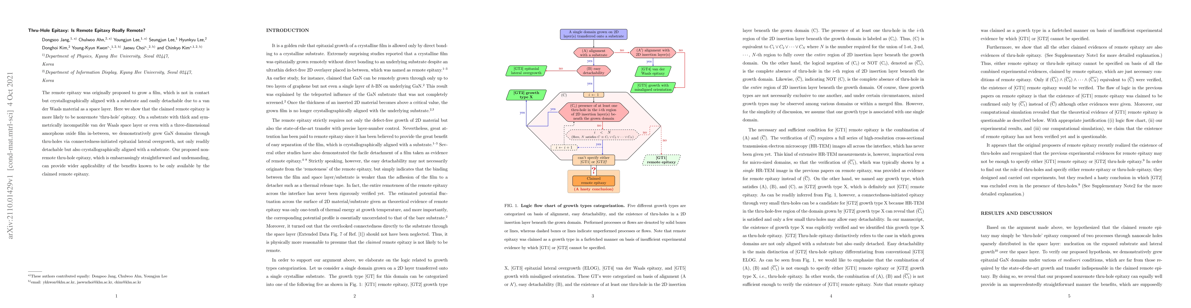
The remote epitaxy was originally proposed to grow a film, which is not in contact but crystallographically aligned with a substrate and easily detachable due to a van der Waals material as a space ...
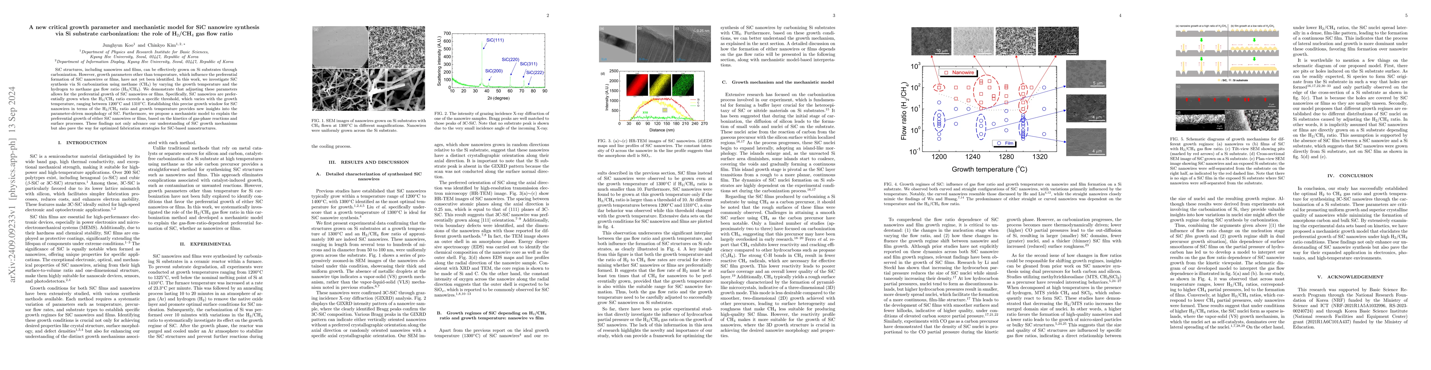
SiC structures, including nanowires and films, can be effectively grown on Si substrates through carbonization. However, growth parameters other than temperature, which influence the preferential form...
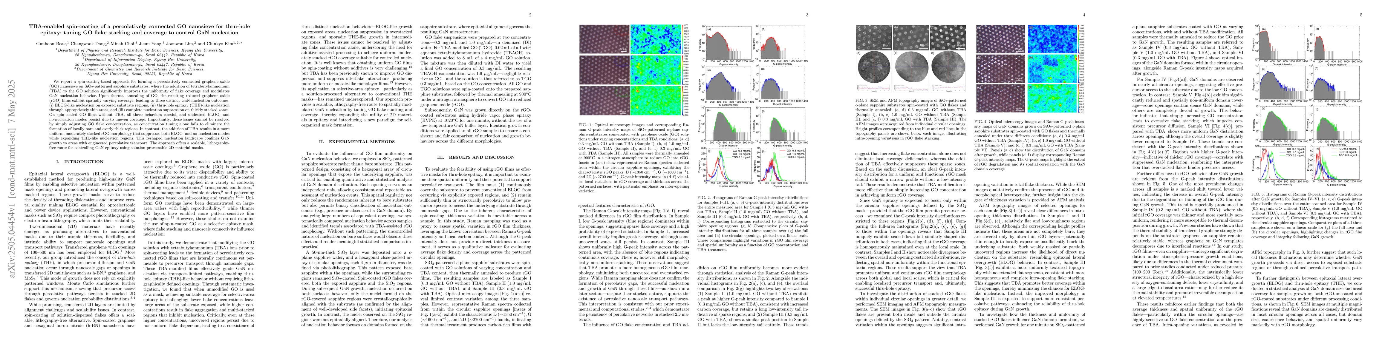
We report a spin-coating-based approach for forming a percolatively connected graphene oxide (GO) nanosieve on SiO$_2$-patterned sapphire substrates, where the addition of tetrabutylammonium (TBA) to ...
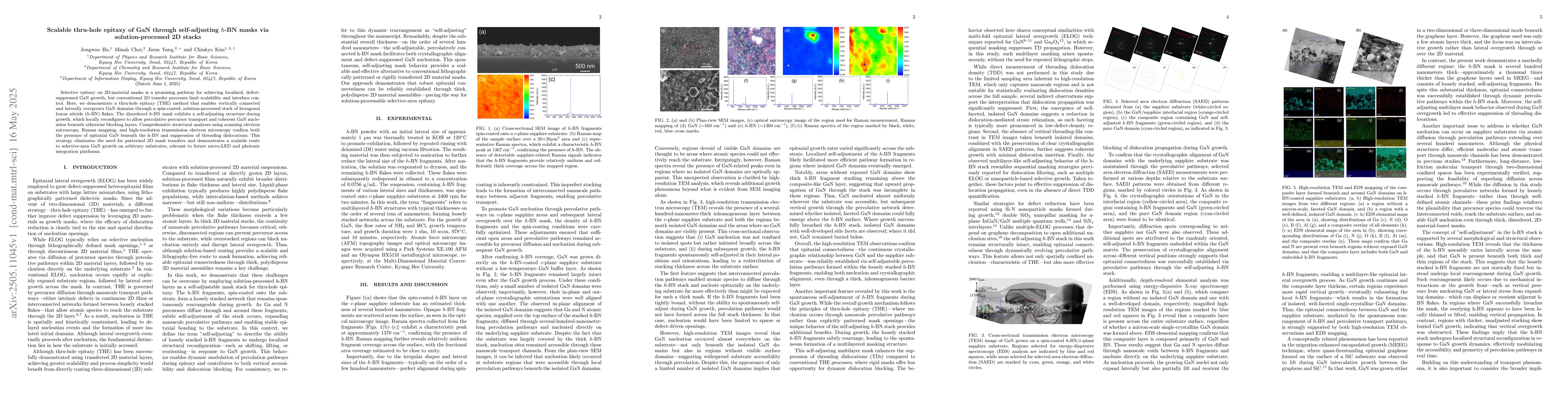
Selective epitaxy on 2D-material masks is a promising pathway for achieving localized, defect-suppressed GaN growth, but conventional 2D transfer processes limit scalability and interface control. Her...
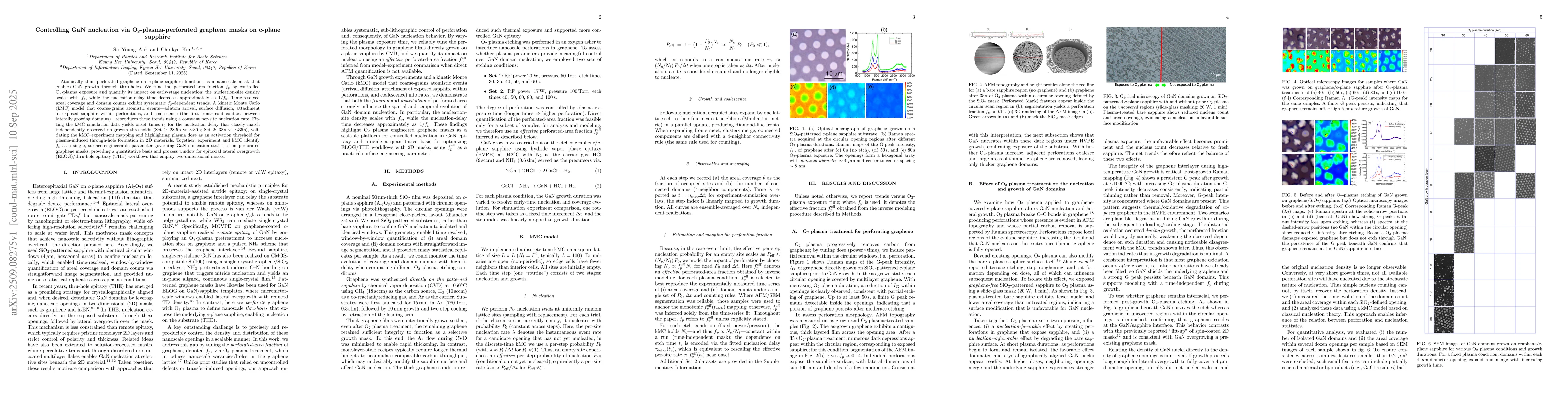
Atomically thin, perforated graphene on $c$-plane sapphire functions as a nanoscale mask that enables GaN growth through thru-holes. We tune the perforated-area fraction $f_p$ by controlled O$_2$-plas...
GaN polarity inversion and the associated inversion domain boundaries (IDBs) are frequently observed during lateral overgrowth and are often discussed in terms of the small energetic spread among comp...
The growth temperature of directly grown boron-compound masks on patterned sapphire can modify the local accessibility of the underlying sapphire surface and thereby alter the subsequent nucleation be...