ArxivLens
C
Researcher

Christian E. N. Petersen

7 papers on arXiv

7 arXiv Papers
5 Total Publications
Profile

Academic Profile

Name Christian E N Petersen
Total Papers 5
Scholar Profile View on Semantic Scholar
Metrics

Statistics

7 arXiv Papers
5 Total Publications
Publications

Papers on arXiv

Thumbnail for Statistical Reproducibility of Selective Area Grown InAs Nanowire
  Devices
arXiv
Statistical Reproducibility of Selective Area Grown InAs Nanowire Devices

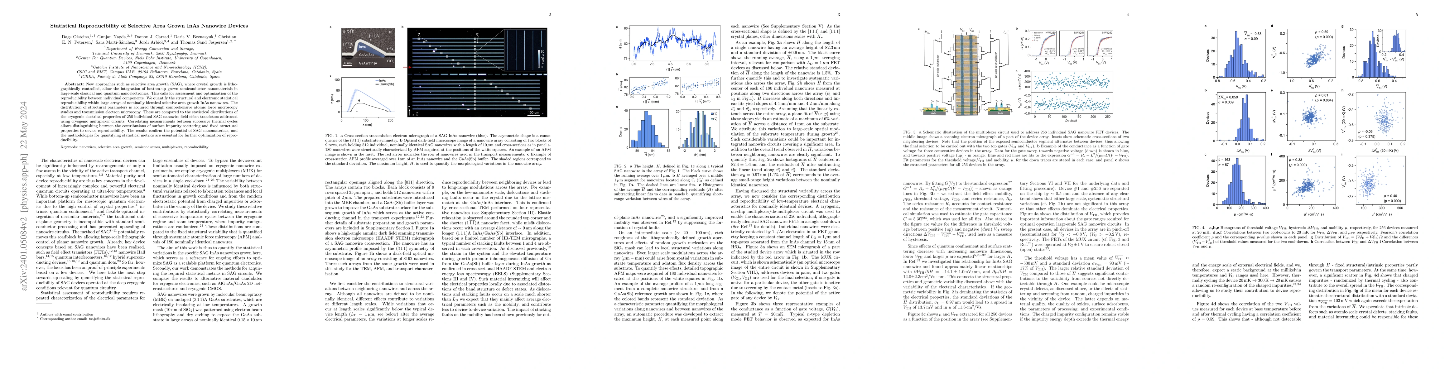
New approaches such as selective area growth, where crystal growth is lithographically controlled, allow the integration of bottom-up grown semiconductor nanomaterials in large-scale classical and q...

Thumbnail for Cryogenic Multiplexing with Bottom-Up Nanowires
arXiv
Cryogenic Multiplexing with Bottom-Up Nanowires

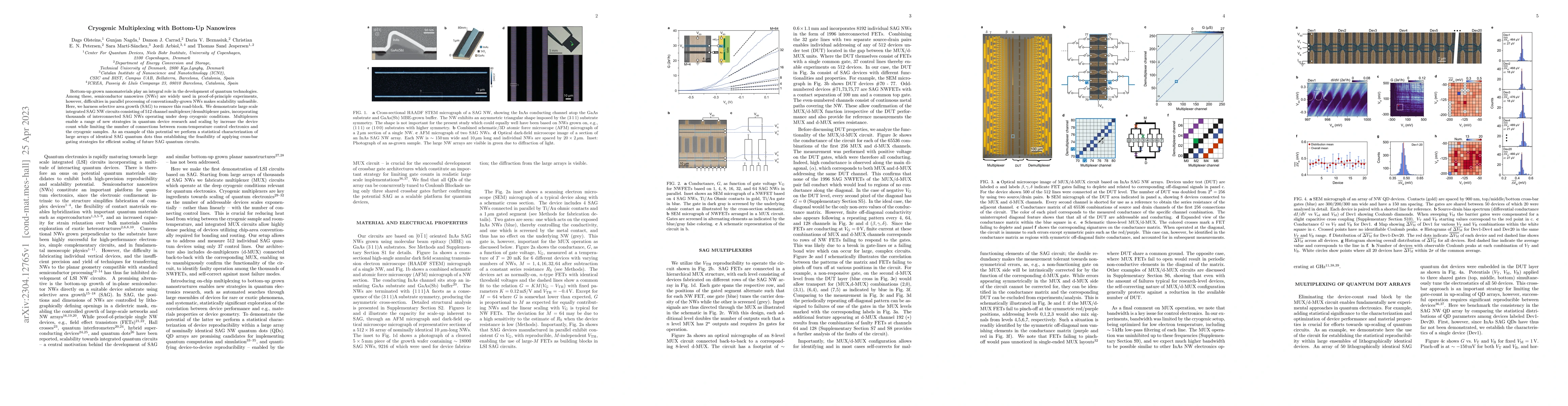
Bottom-up grown nanomaterials play an integral role in the development of quantum technologies. Among these, semiconductor nanowires (NWs) are widely used in proof-of-principle experiments, however,...

Thumbnail for Photon assisted tunneling of high order multiple Andreev reflections in
  epitaxial nanowire Josephson junctions
arXiv
Photon assisted tunneling of high order multiple Andreev reflections in epitaxial nanowire Josephson junctions

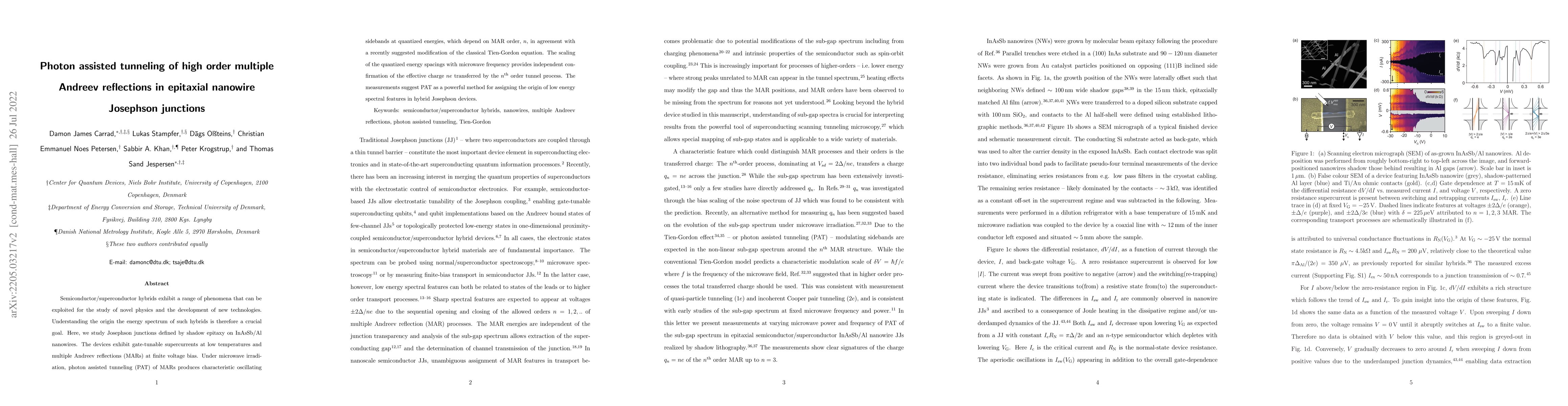
Semiconductor/superconductor hybrids exhibit a range of phenomena that can be exploited for the study of novel physics and the development of new technologies. Understanding the origin the energy sp...

Thumbnail for Andreev interference in the surface accumulation layer of half-shell
  InAsSb/Al hybrid nanowires
arXiv
Andreev interference in the surface accumulation layer of half-shell InAsSb/Al hybrid nanowires

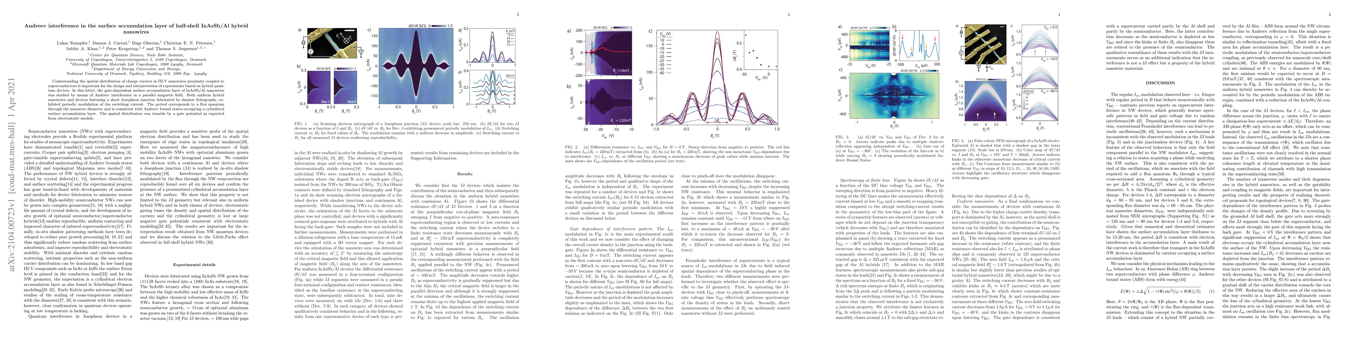
Understanding the spatial distribution of charge carriers in III-V nanowires proximity coupled to superconductors is important for the design and interpretation of experiments based on hybrid quantu...

Thumbnail for $μ_\mathrm{2T}(n)$: A Method for Extracting the Density Dependent
  Mobility in Two-Terminal Nanodevices
arXiv
$μ_\mathrm{2T}(n)$: A Method for Extracting the Density Dependent Mobility in Two-Terminal Nanodevices

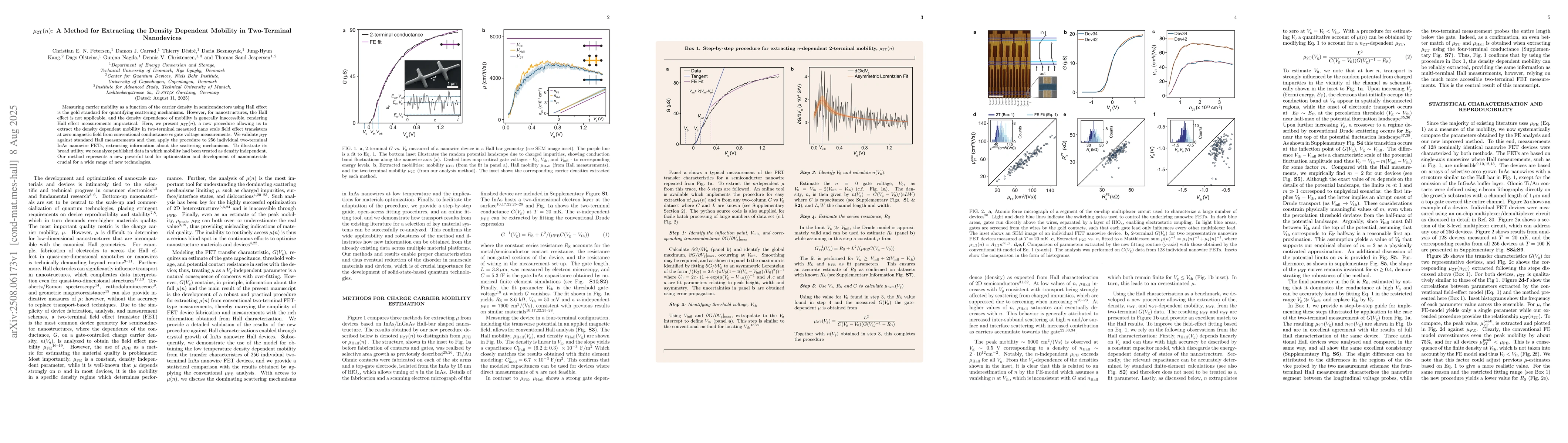
Measuring carrier mobility as a function of the carrier density in semiconductors using Hall effect is the gold standard for quantifying scattering mechanisms. However, for nanostructures, the Hall ef...

Thumbnail for Cryogenic performance of field-effect transistors and amplifiers based
  on selective area grown InAs nanowires
arXiv
Cryogenic performance of field-effect transistors and amplifiers based on selective area grown InAs nanowires

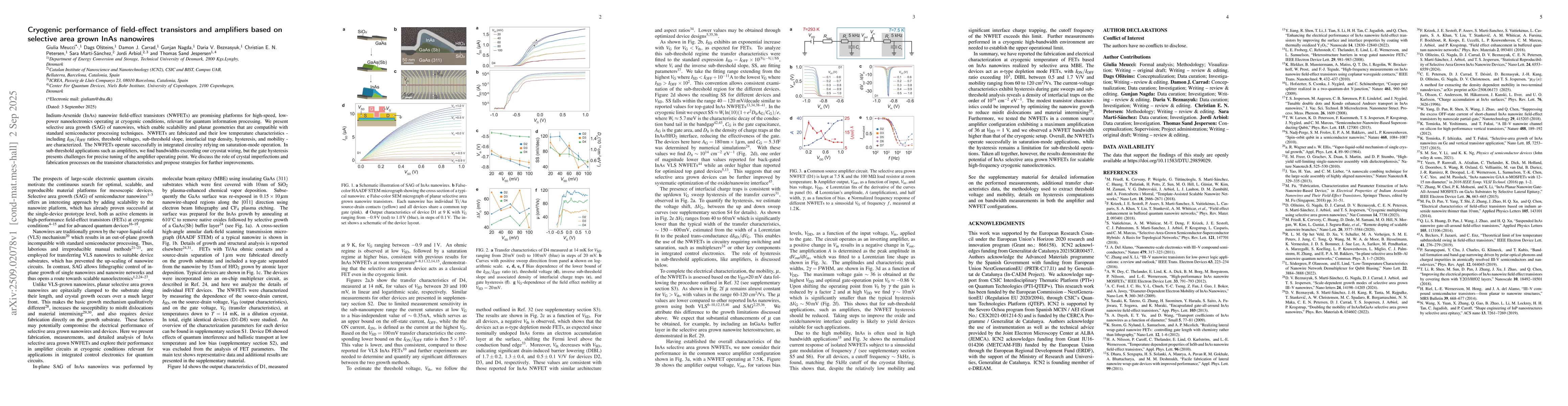
Indium-Arsenide (InAs) nanowire field-effect transistors (NWFETs) are promising platforms for high-speed, low power nanoelectronics operating at cryogenic conditions, relevant for quantum information ...

Thumbnail for Tomography of Transport Pathways in Selective-Area-Grown Nanowires Using Angle-Resolved Conductance Fluctuations
arXiv
Tomography of Transport Pathways in Selective-Area-Grown Nanowires Using Angle-Resolved Conductance Fluctuations

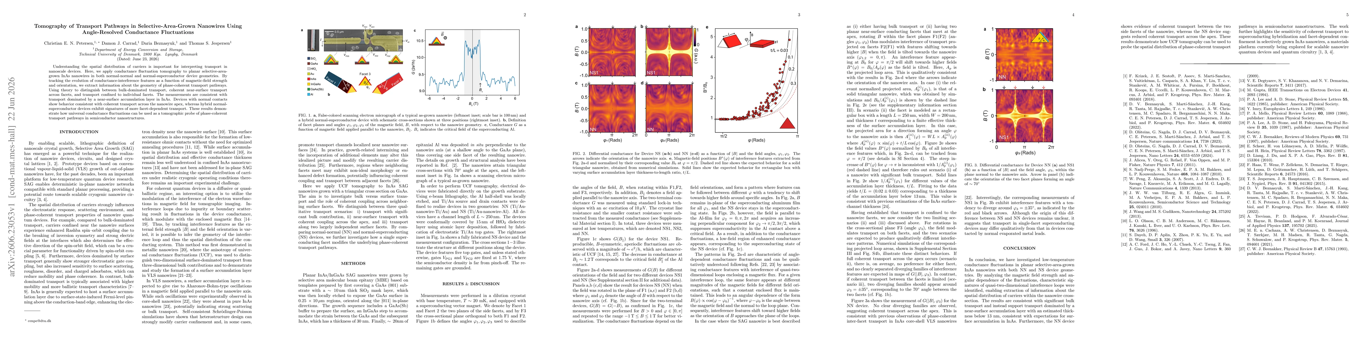
Understanding the spatial distribution of carriers is important for interpreting transport in nanoscale devices. Here, we apply conductance fluctuation tomography to planar selective-area-grown InAs n...

This website uses cookies to ensure you get the best experience. Learn more