Academic Profile
Statistics
Similar Authors
Papers on arXiv
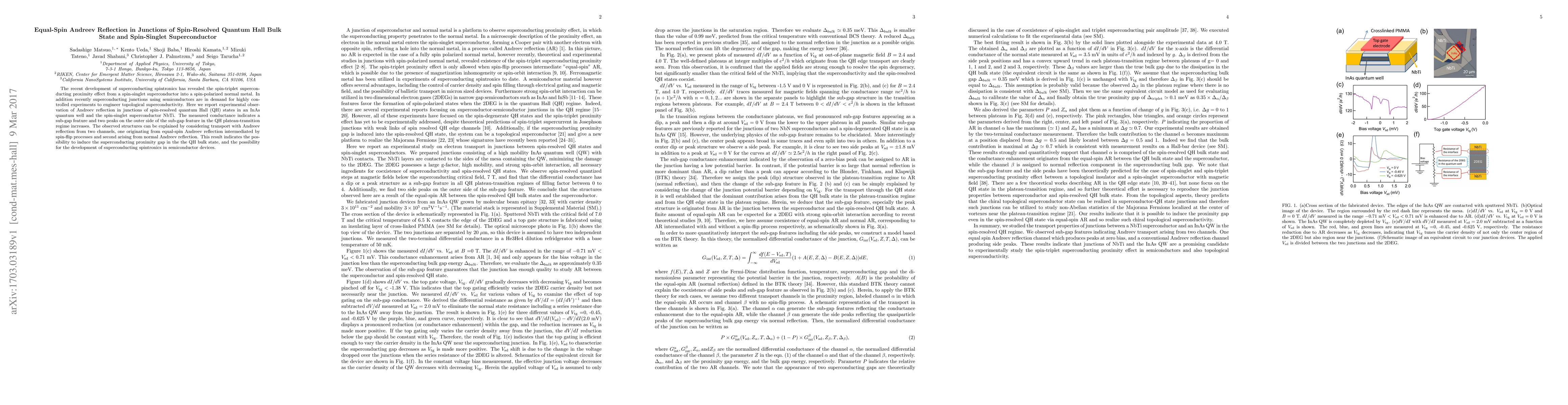
The recent development of superconducting spintronics has revealed the spin-triplet superconducting proximity effect from a spin-singlet superconductor into a spin-polarized normal metal. In additio...
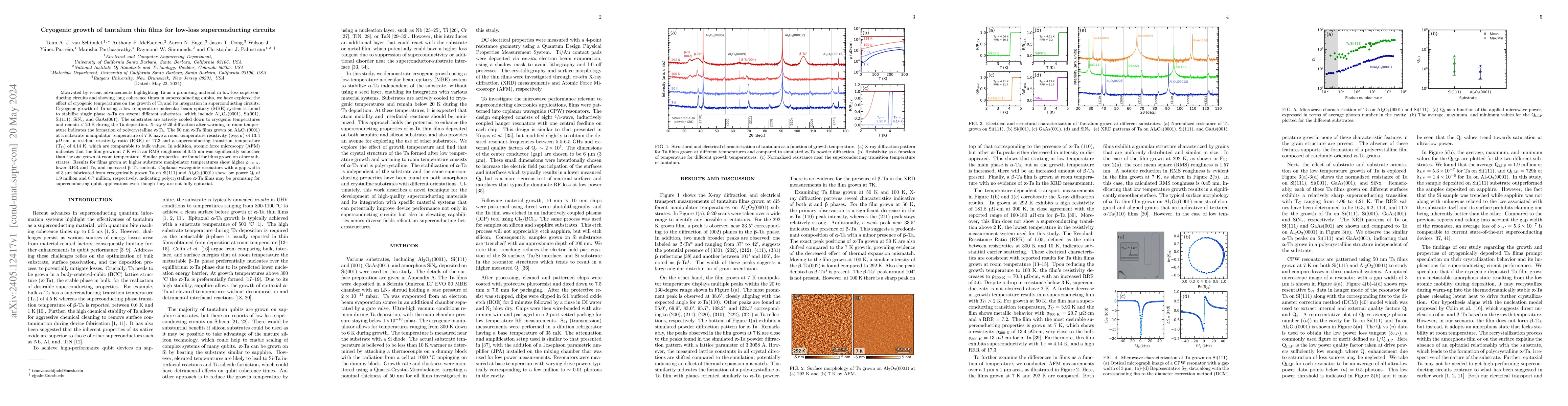
Motivated by recent advancements highlighting Ta as a promising material in low-loss superconducting circuits and showing long coherence times in superconducting qubits, we have explored the effect ...
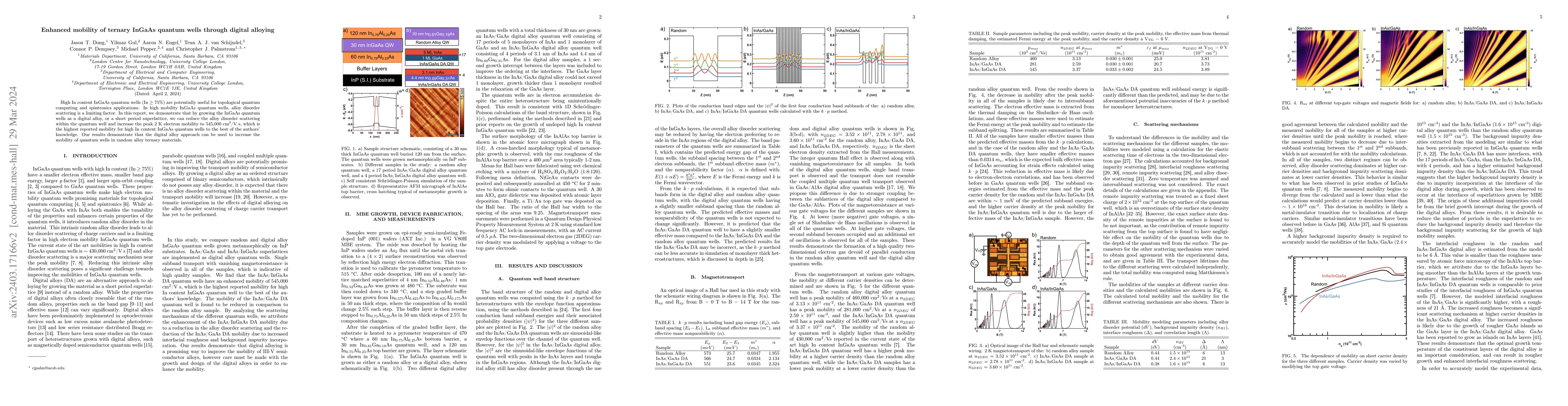
High In content InGaAs quantum wells (In $\geq$ 75%) are potentially useful for topological quantum computing and spintronics applications. In high mobility InGaAs quantum wells, alloy disorder scat...
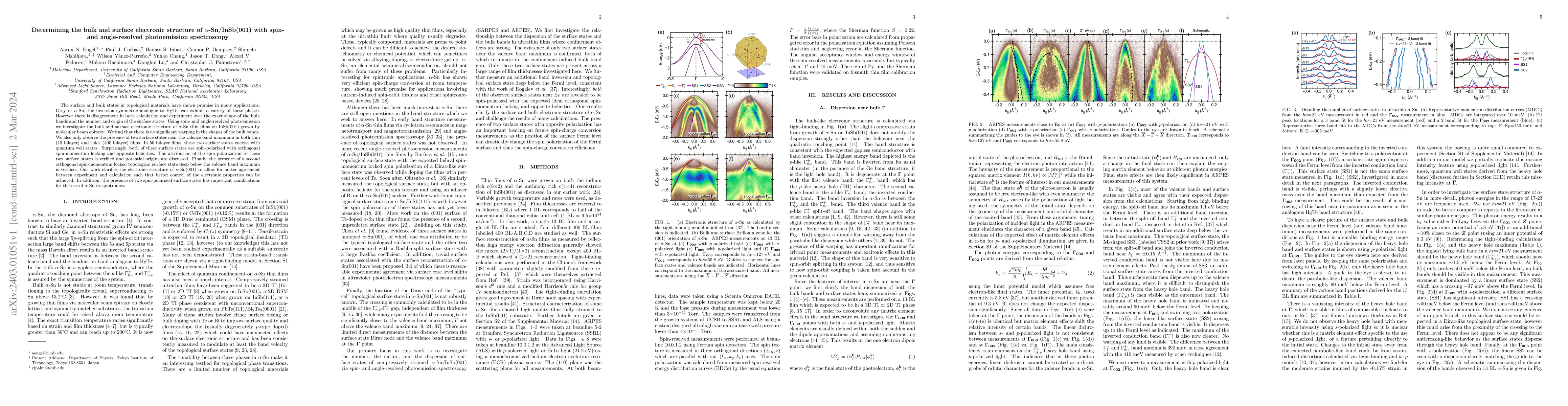
The surface and bulk states in topological materials have shown promise in many applications. Grey or $\alpha$-Sn, the inversion symmetric analogue to HgTe, can exhibit a variety of these phases. Ho...
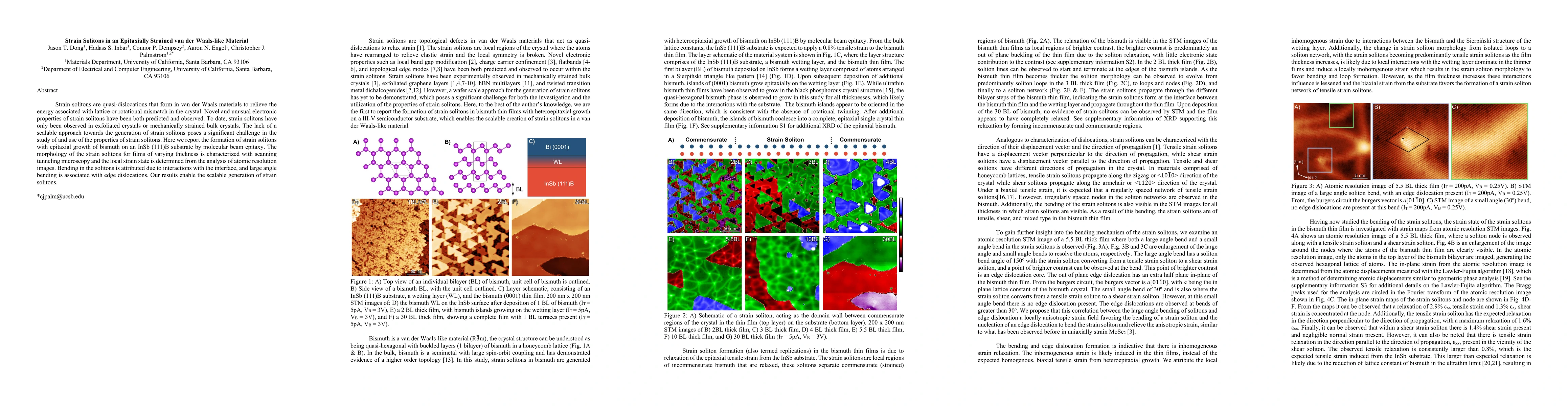
Strain solitons are quasi-dislocations that form in van der Waals materials to relieve the energy associated with lattice or rotational mismatch in the crystal. Novel and unusual electronic properti...
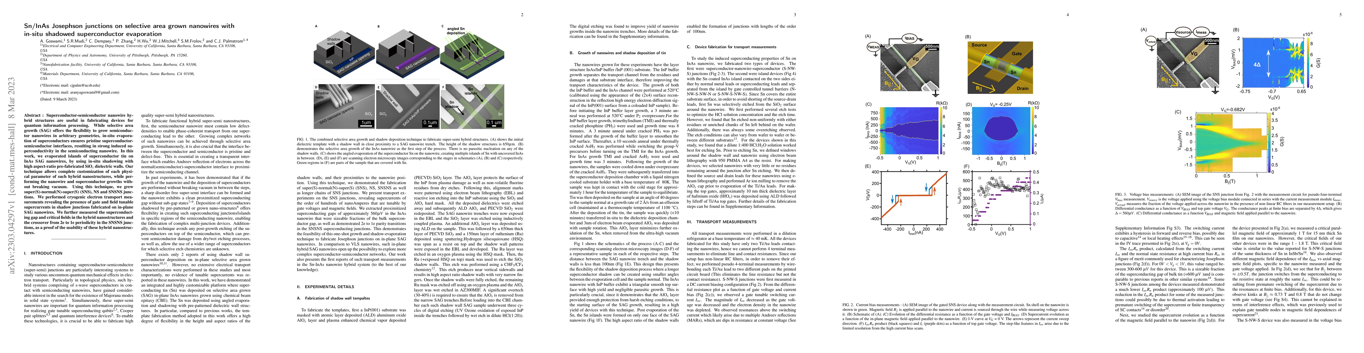
Superconductor-semiconductor nanowire hybrid structures are useful in fabricating devices for quantum information processing. While selective area growth (SAG) offers the flexibility to grow semicon...
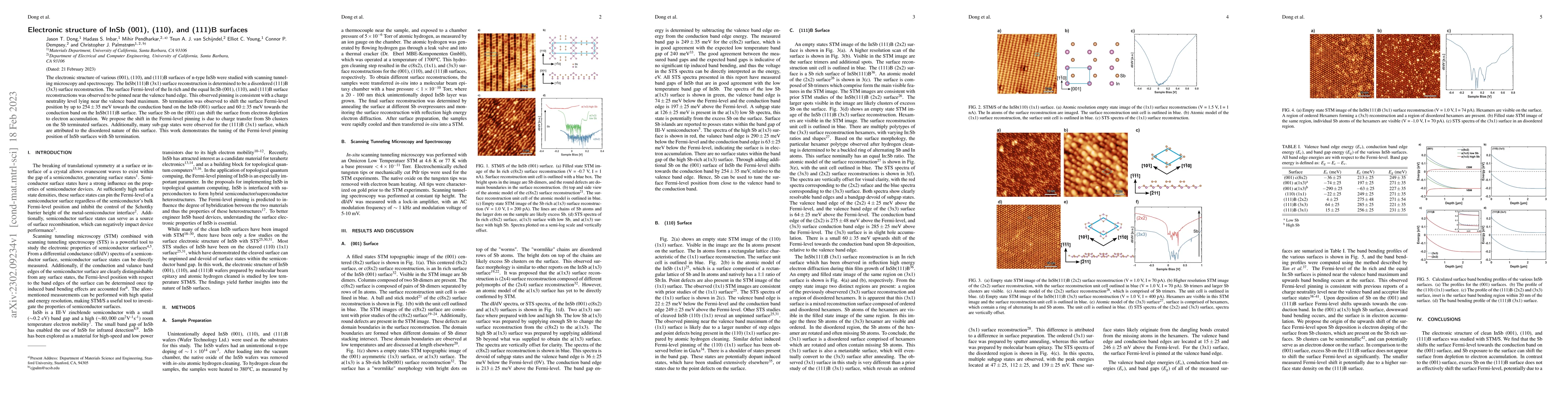
The electronic structure of various (001), (110), and (111)B surfaces of n-type InSb were studied with scanning tunneling microscopy and spectroscopy. The InSb(111)B (3x1) surface reconstruction is ...
Rare-earth monopnictide (RE-V) semimetal crystals subjected to hydrostatic pressure have shown interesting trends in magnetoresistance, magnetic ordering, and superconductivity, with theory predicti...
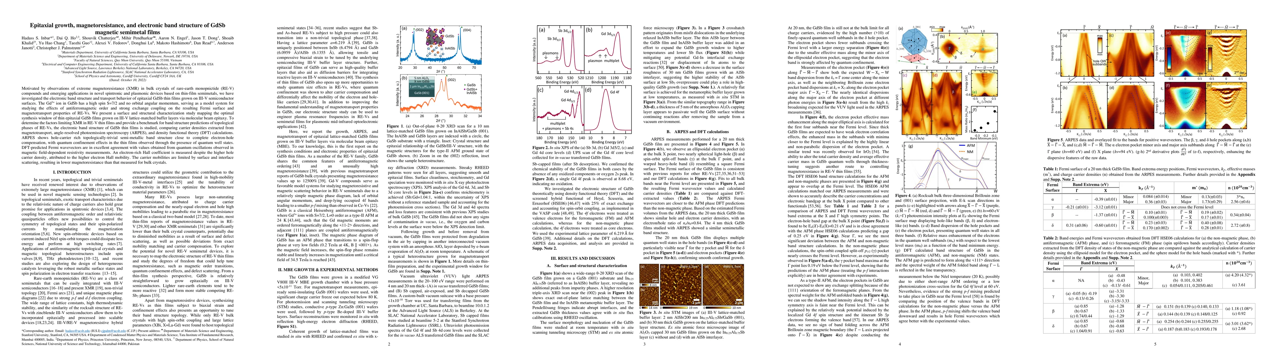
Motivated by observations of extreme magnetoresistance (XMR) in bulk crystals of rare-earth monopnictide (RE-V) compounds and emerging applications in novel spintronic and plasmonic devices based on...
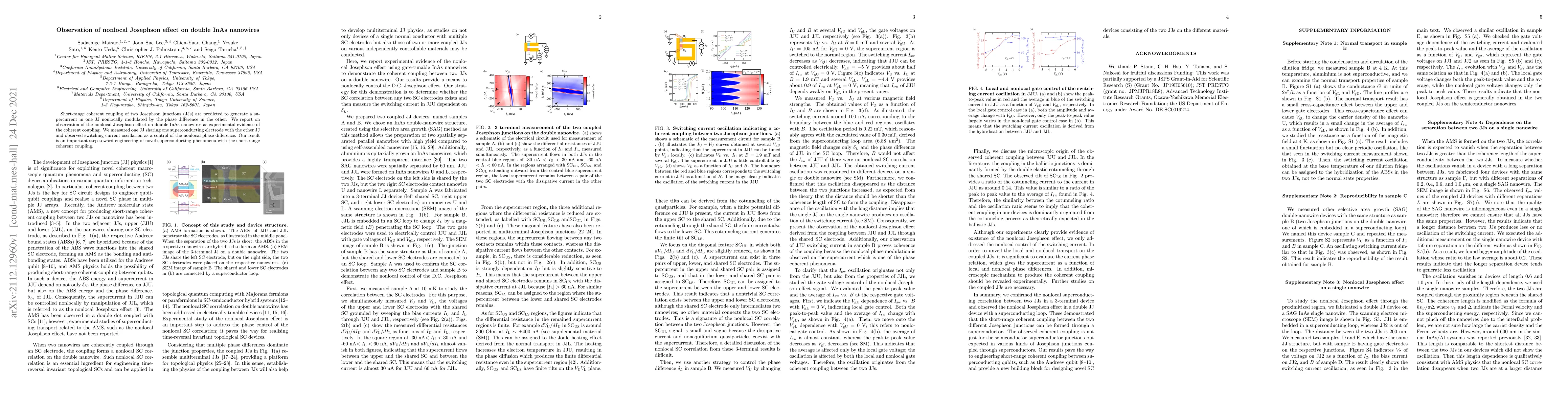
Short-range coherent coupling of two Josephson junctions (JJs) are predicted to generate a supercurrent in one JJ nonlocally modulated by the phase difference in the other. We report on observation ...
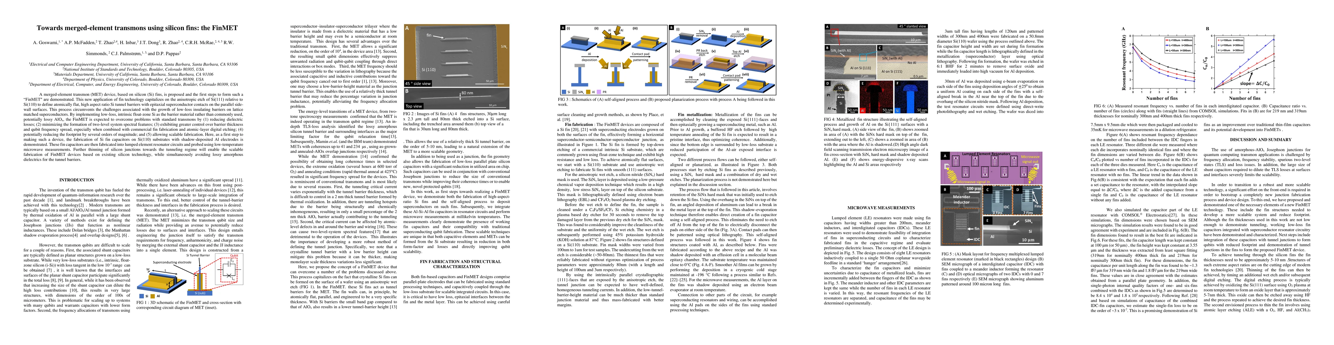
A merged-element transmon (MET) device, based on silicon (Si) fins, is proposed and the first steps to form such a "FinMET" are demonstrated. This new application of fin technology capitalizes on th...
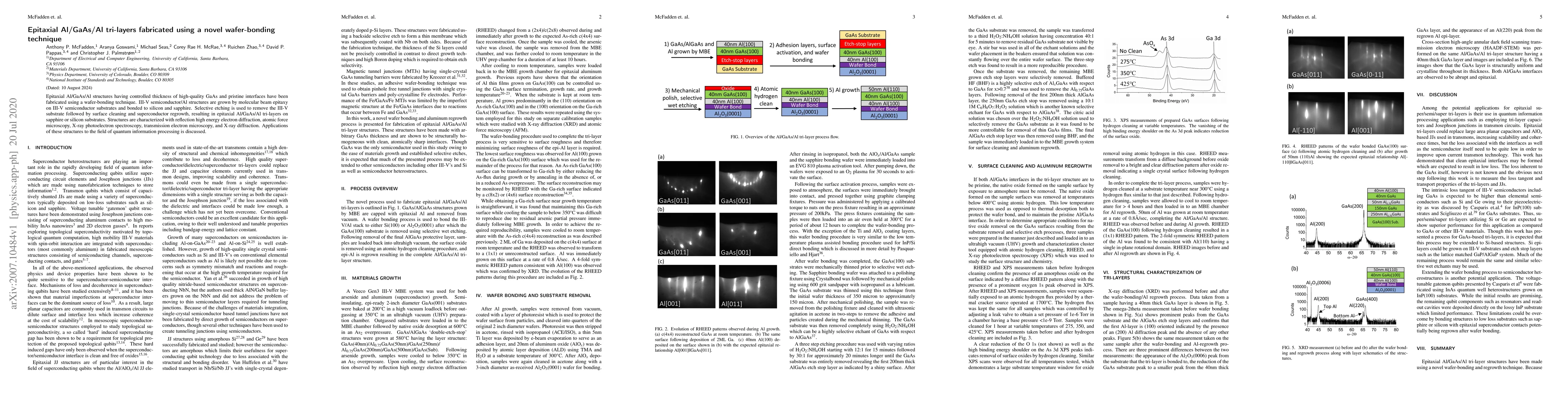
Epitaxial Al/GaAs/Al structures having controlled thickness of high-quality GaAs and pristine interfaces have been fabricated using a wafer-bonding technique. III-V semiconductor/Al structures are g...
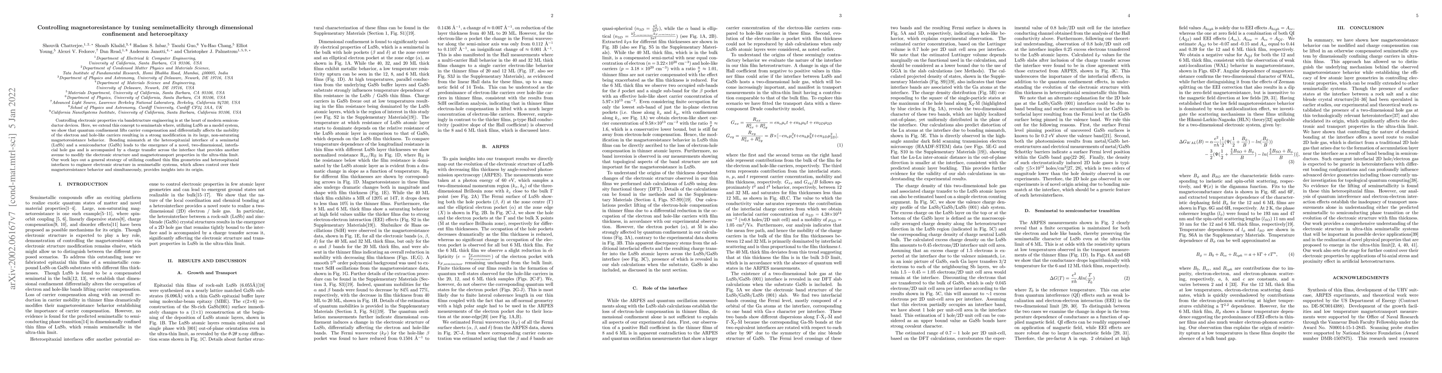
Controlling the electronic properties via bandstructure engineering is at the heart of modern semiconductor devices. Here, we extend this concept to semimetals where, utilizing LuSb as a model syste...
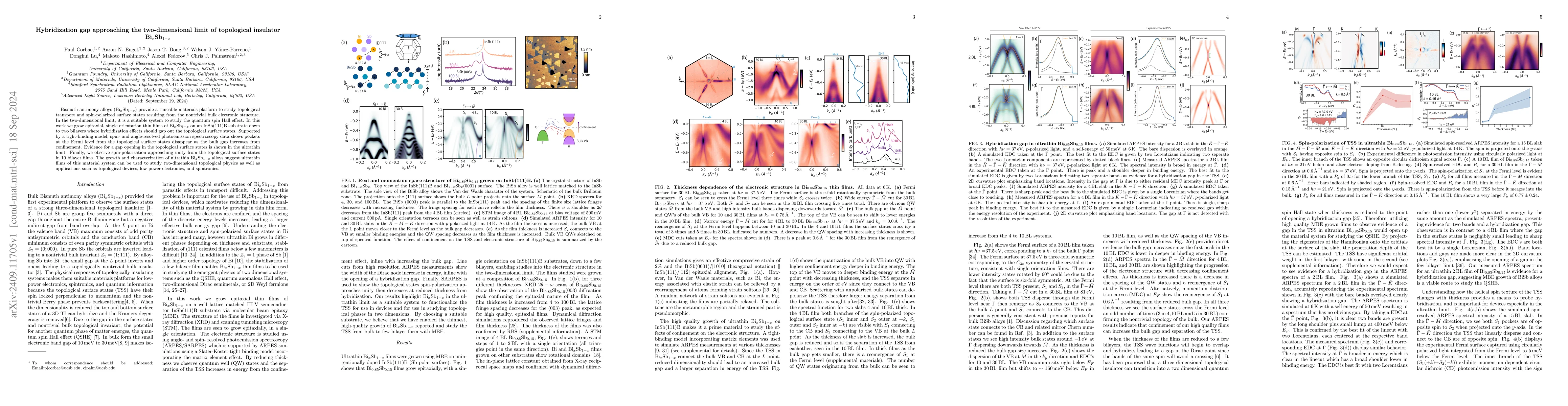
Bismuth antimony alloys (Bi$_x$Sb$_{1-x}$) provide a tuneable materials platform to study topological transport and spin-polarized surface states resulting from the nontrivial bulk electronic structur...
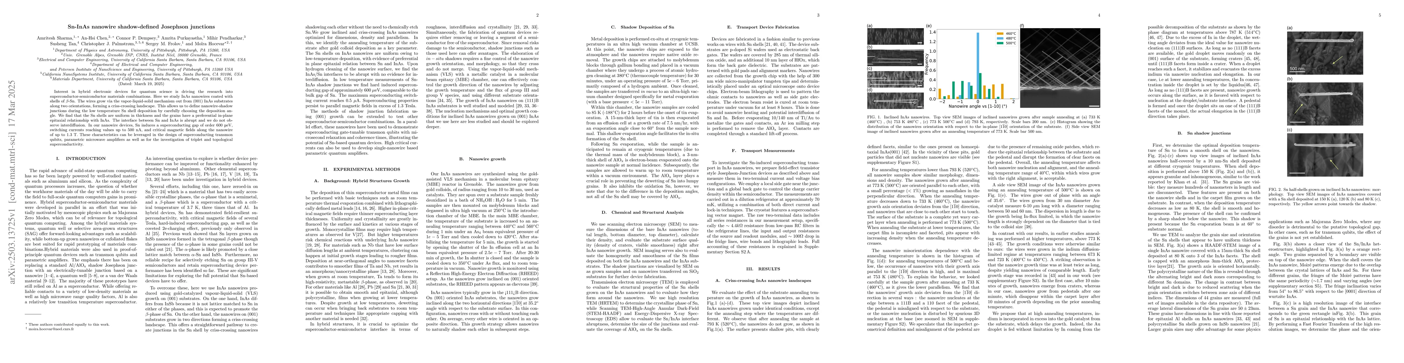
Interest in hybrid electronic devices for quantum science is driving the research into superconductor-semiconductor materials combinations. Here we study InAs nanowires coated with shells of $\beta$-S...
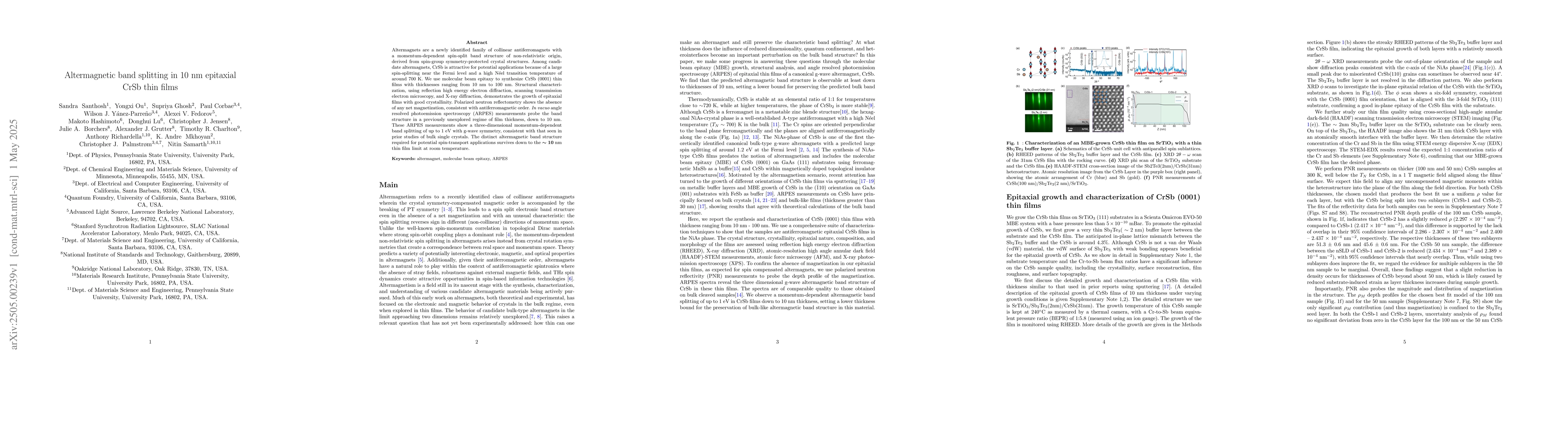
Altermagnets are a newly identified family of collinear antiferromagnets with momentum-dependent spin-split band structure of non-relativistic origin, derived from spin-group symmetry-protected crysta...
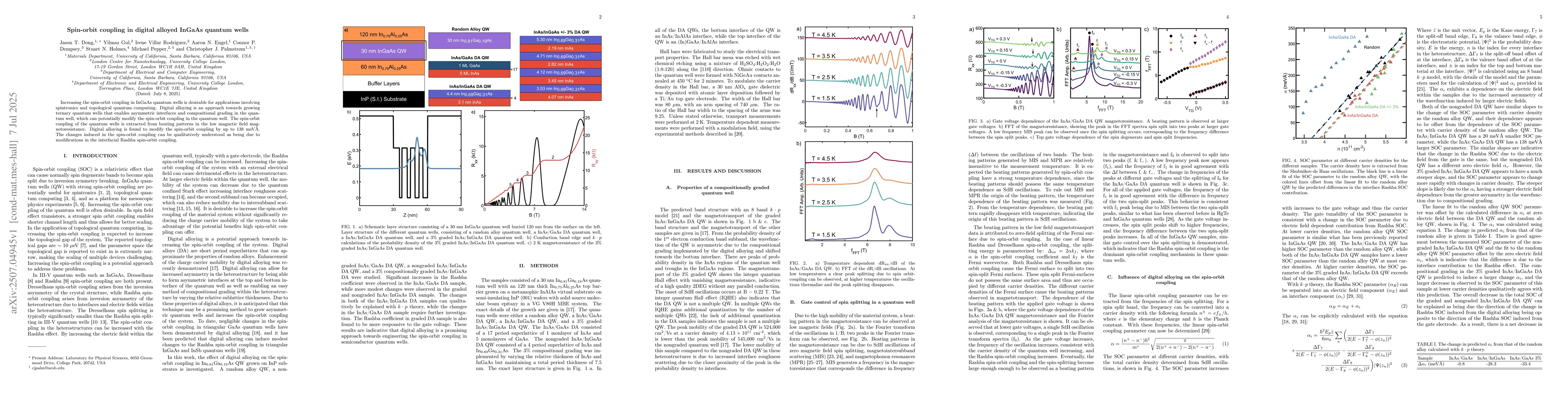
Increasing the spin-orbit coupling in InGaAs quantum wells is desirable for applications involving spintronics and topological quantum computing. Digital alloying is an approach towards growing ternar...
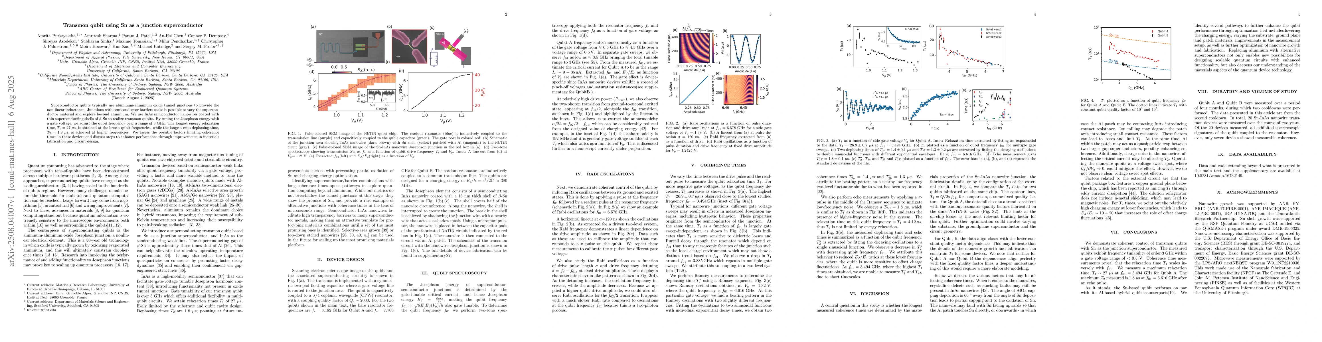
Superconductor qubits typically use aluminum-aluminum oxide tunnel junctions to provide the non-linear inductance. Junctions with semiconductor barriers make it possible to vary the superconductor mat...
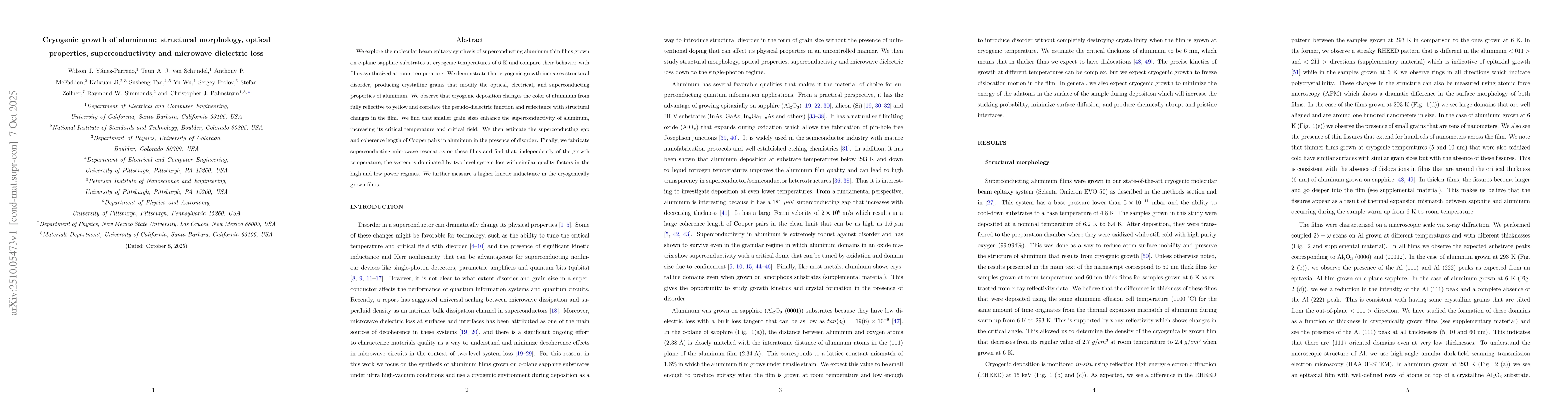
We explore the molecular beam epitaxy synthesis of superconducting aluminum thin films grown on c-plane sapphire substrates at cryogenic temperatures of 6 K and compare their behavior with films synth...
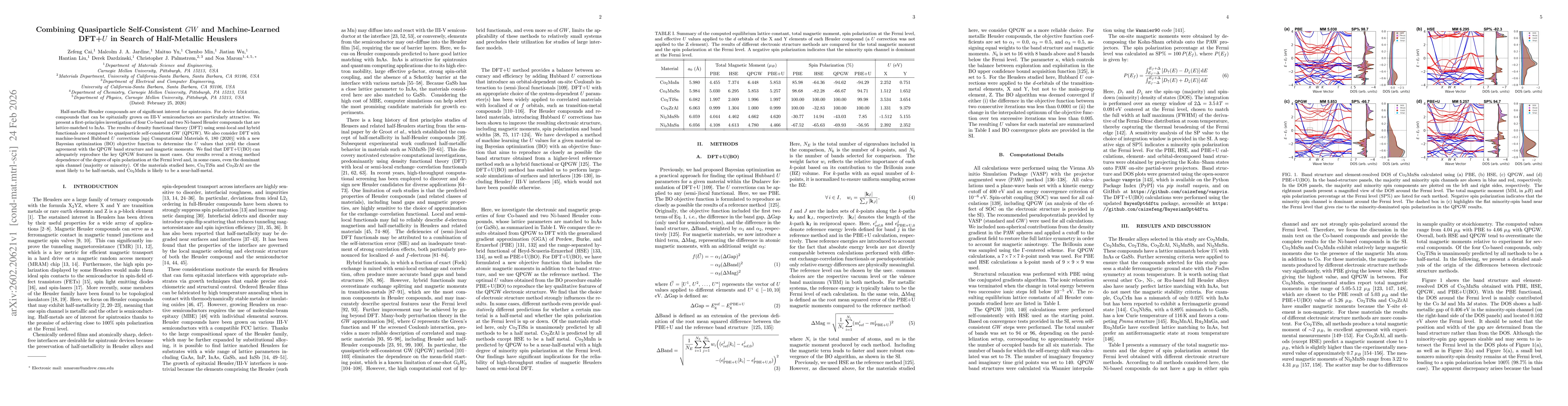
Half-metallic Heusler compounds are of significant interest for spintronics. For device fabrication, compounds that can be epitaxially grown on III-V semiconductors are particularly attractive. We pre...
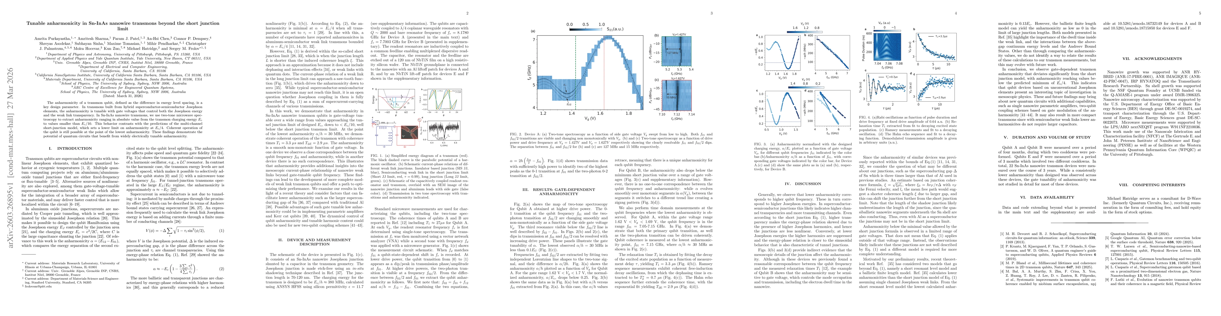
The anharmonicity of a transmon qubit, defined as the difference in energy level spacing, is a key design parameter. In transmons built from hybrid superconductor-semiconductor Josephson elements, the...
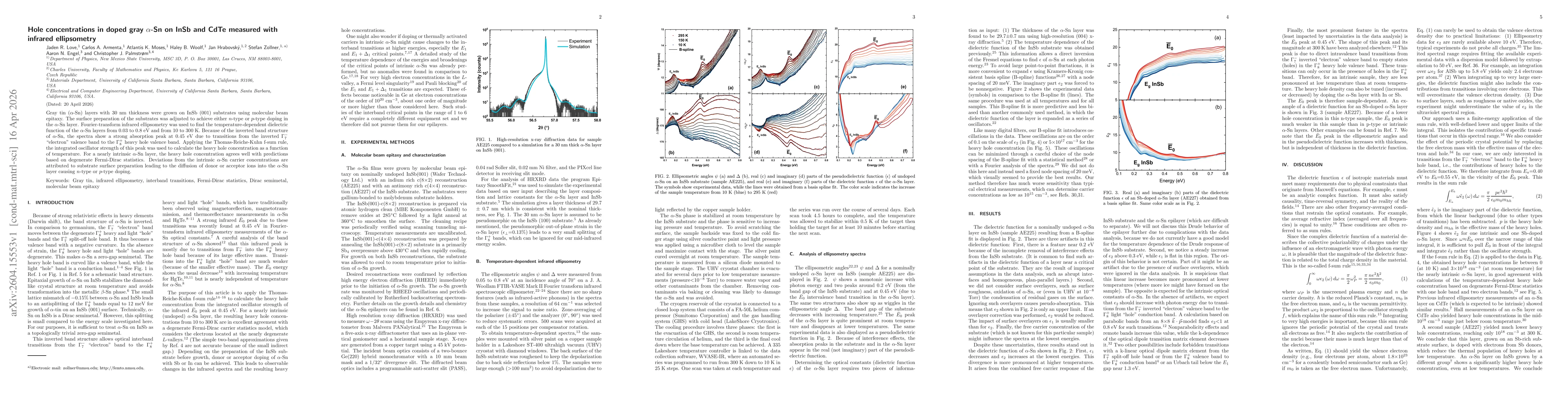
Gray tin (α-Sn) layers with 30 nm thickness were grown on InSb (001) substrates using molecular beam epitaxy. The surface preparation of the substrates was adjusted to achieve either n-type or p-type ...