D. Frank Ogletree

12 papers on arXiv

Academic Profile

Name: F. Ogletree
Total Papers: 16

Statistics

arXiv Papers 12
Total Publications 16

Papers on arXiv

Thumbnail for Observation of charge density wave order in 1D mirror twin boundaries of
  single-layer MoSe2

Observation of charge density wave order in 1D mirror twin boundaries of single-layer MoSe2

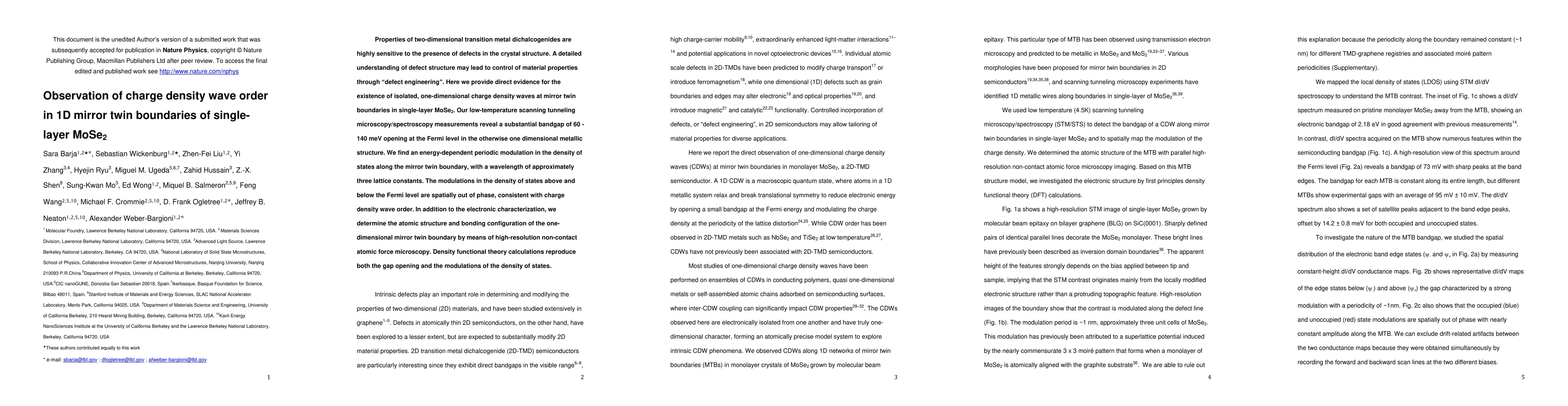
Properties of two-dimensional transition metal dichalcogenides are highly sensitive to the presence of defects in the crystal structure. A detailed understanding of defect structure may lead to cont...

Thumbnail for A substitutional quantum defect in WS$_2$ discovered by high-throughput
  computational screening and fabricated by site-selective STM manipulation

A substitutional quantum defect in WS$_2$ discovered by high-throughput computational screening and fabricated by site-selective STM manipulation

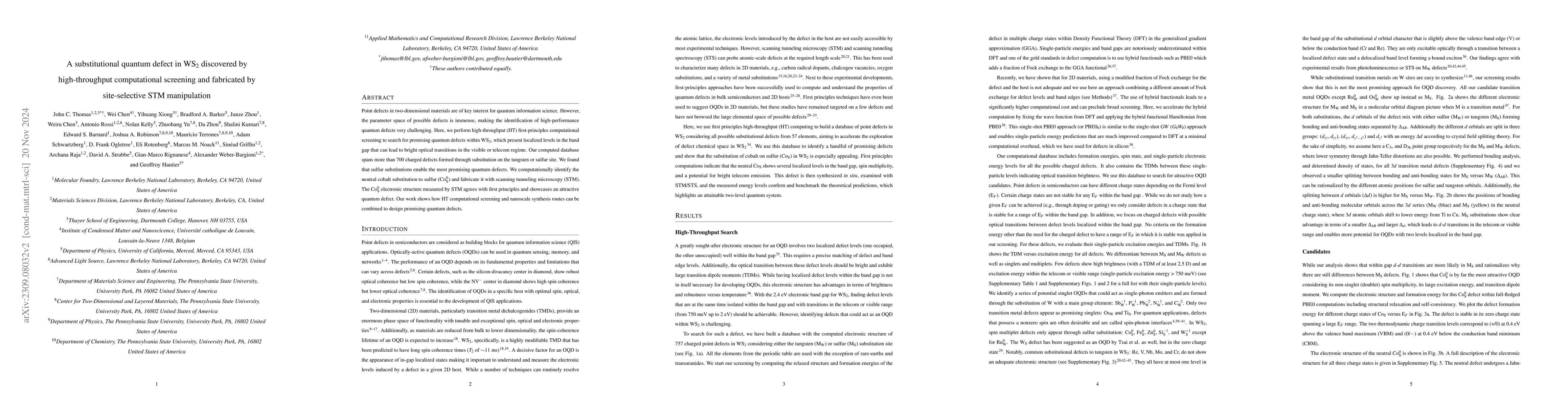
Point defects in two-dimensional materials are of key interest for quantum information science. However, the space of possible defects is immense, making the identification of high-performance quant...

Thumbnail for WS$_2$ Band Gap Renormalization Induced by Tomonaga Luttinger Liquid
  Formation in Mirror Twin Boundaries

WS$_2$ Band Gap Renormalization Induced by Tomonaga Luttinger Liquid Formation in Mirror Twin Boundaries

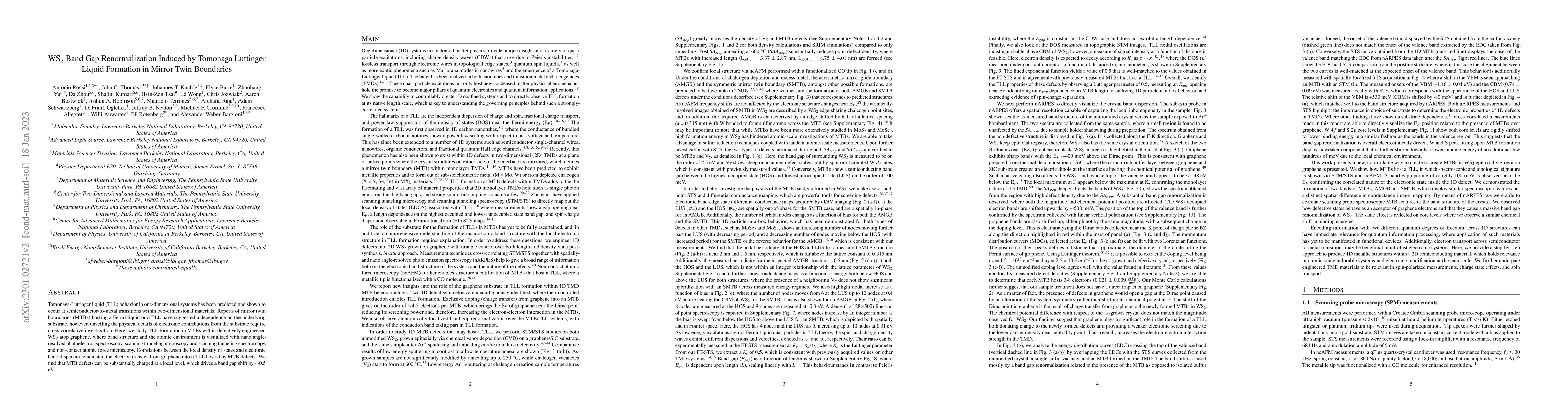
Tomonaga-Luttinger liquid (TLL) behavior in one-dimensional systems has been predicted and shown to occur at semiconductor-to-metal transitions within two-dimensional materials. Reports of mirror tw...

Thumbnail for Superconducting Niobium Tip Electron Beam Source

Superconducting Niobium Tip Electron Beam Source

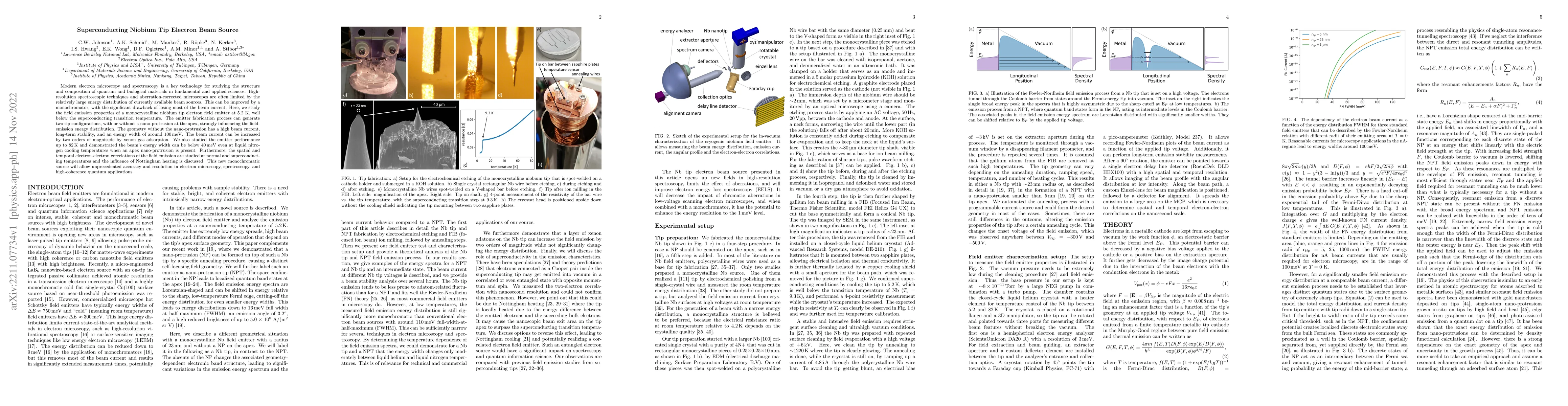
Modern electron microscopy and spectroscopy is a key technology for studying the structure and composition of quantum and biological materials in fundamental and applied sciences. High-resolution sp...

Thumbnail for Effects of Laser-Annealing on Fixed-Frequency Superconducting Qubits

Effects of Laser-Annealing on Fixed-Frequency Superconducting Qubits

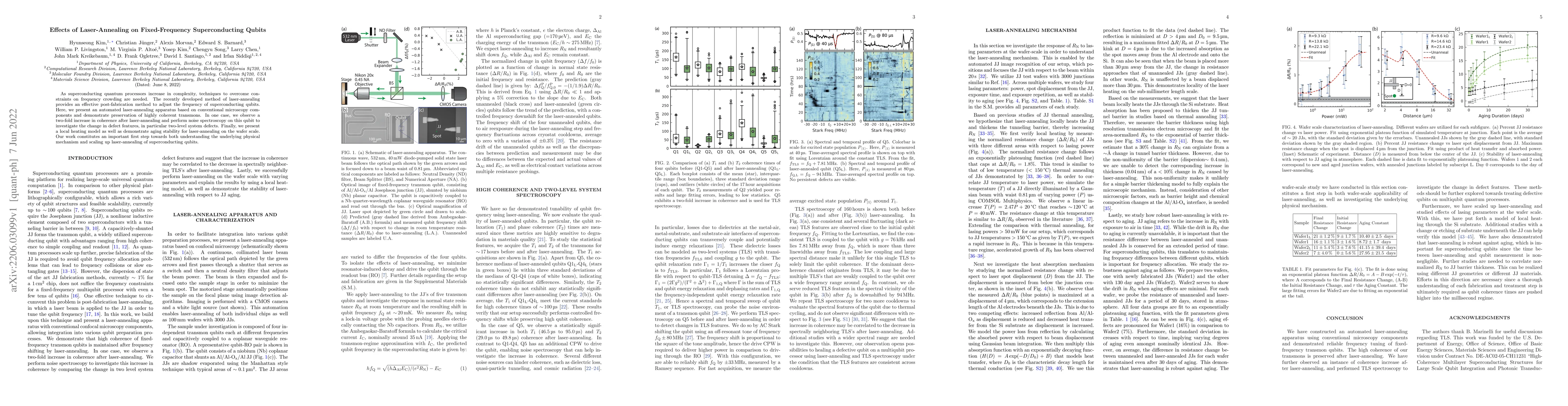
As superconducting quantum processors increase in complexity, techniques to overcome constraints on frequency crowding are needed. The recently developed method of laser-annealing provides an effect...

Thumbnail for Near-monochromatic tuneable cryogenic niobium electron field emitter

Near-monochromatic tuneable cryogenic niobium electron field emitter

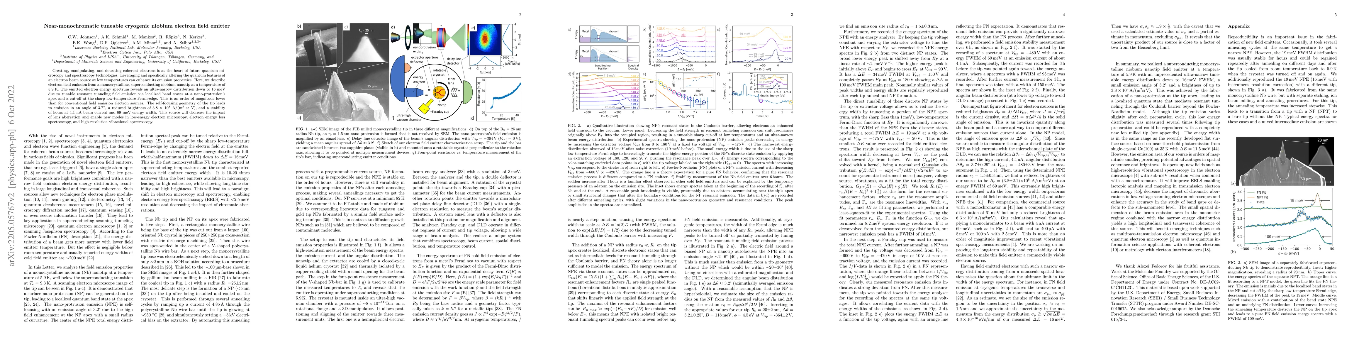
Creating, manipulating, and detecting coherent electrons is at the heart of future quantum microscopy and spectroscopy technologies. Leveraging and specifically altering the quantum features of an e...

Thumbnail for Microscopic Theory of Magnetic Disorder-Induced Decoherence in
  Superconducting Nb Films

Microscopic Theory of Magnetic Disorder-Induced Decoherence in Superconducting Nb Films

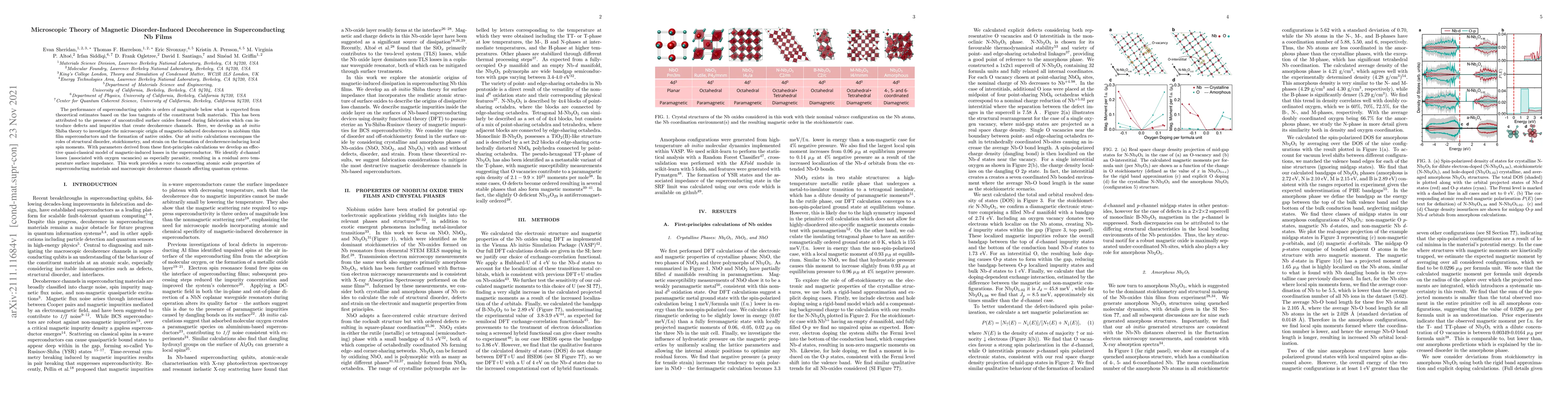
The performance of superconducting qubits is orders of magnitude below what is expected from theoretical estimates based on the loss tangents of the constituent bulk materials. This has been attribu...

Thumbnail for Elucidating the local atomic and electronic structure of amorphous
  oxidized superconducting niobium films

Elucidating the local atomic and electronic structure of amorphous oxidized superconducting niobium films

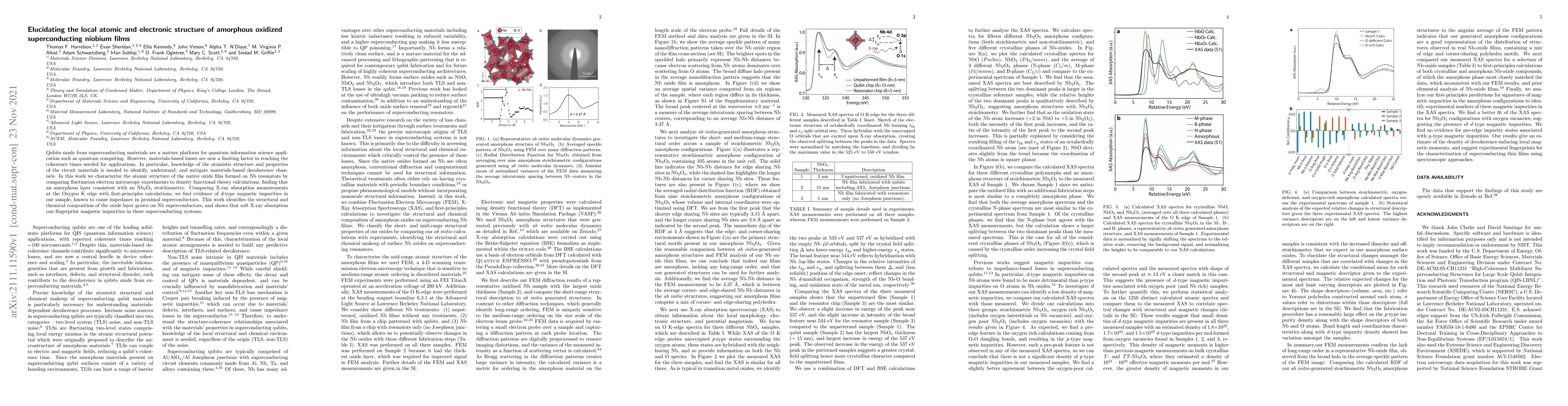
Qubits made from superconducting materials are a mature platform for quantum information science application such as quantum computing. However, materials-based losses are now a limiting factor in r...

Thumbnail for Autonomous Investigations over WS$_2$ and Au{111} with Scanning Probe
  Microscopy

Autonomous Investigations over WS$_2$ and Au{111} with Scanning Probe Microscopy

Individual atomic defects in 2D materials impact their macroscopic functionality. Correlating the interplay is challenging, however, intelligent hyperspectral scanning tunneling spectroscopy (STS) m...

Thumbnail for Localization and reduction of superconducting quantum coherent circuit
  losses

Localization and reduction of superconducting quantum coherent circuit losses

Quantum sensing and computation can be realized with superconducting microwave circuits. Qubits are engineered quantum systems of capacitors and inductors with non-linear Josephson junctions. They o...

Thumbnail for How Substitutional Point Defects in Two-Dimensional WS$_2$ Induce Charge
  Localization, Spin-Orbit Splitting, and Strain

How Substitutional Point Defects in Two-Dimensional WS$_2$ Induce Charge Localization, Spin-Orbit Splitting, and Strain

Control of impurity concentrations in semiconducting materials is essential to device technology. Because of their intrinsic confinement, the properties of two-dimensional semiconductors such as tra...

Thumbnail for Electrically driven photon emission from individual atomic defects in
  monolayer WS2

Electrically driven photon emission from individual atomic defects in monolayer WS2

Optical quantum emitters are a key component of quantum devices for metrology and information processing. In particular, atomic defects in 2D materials can operate as optical quantum emitters that o...

This website uses cookies to ensure you get the best experience. Learn more