Academic Profile
Statistics
Similar Authors
Papers on arXiv
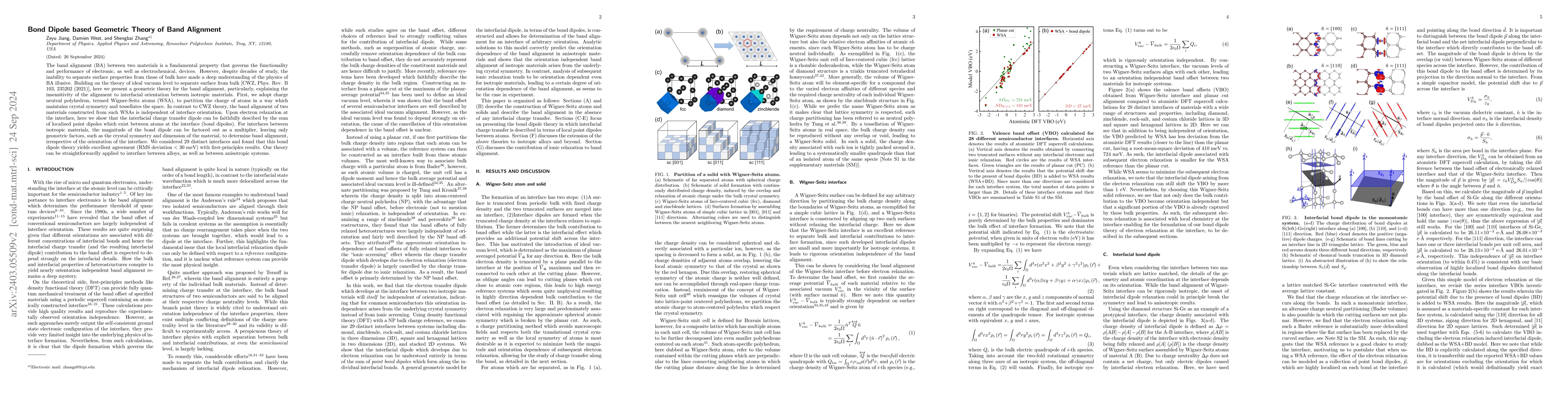
Understanding the band offset between materials is pivotal for electronic device functionality. While traditional theories attribute this offset solely to intrinsic properties of constituent materia...
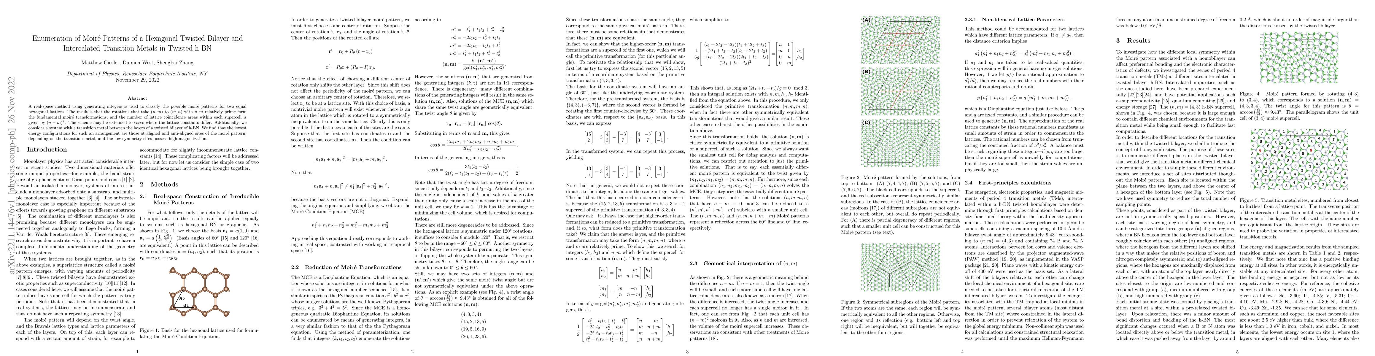
A real-space method using generating integers is used to classify the possible moire patterns for two equal hexagonal lattices. The result is that the rotations that take (n,m) to (m,n) with n,m rel...
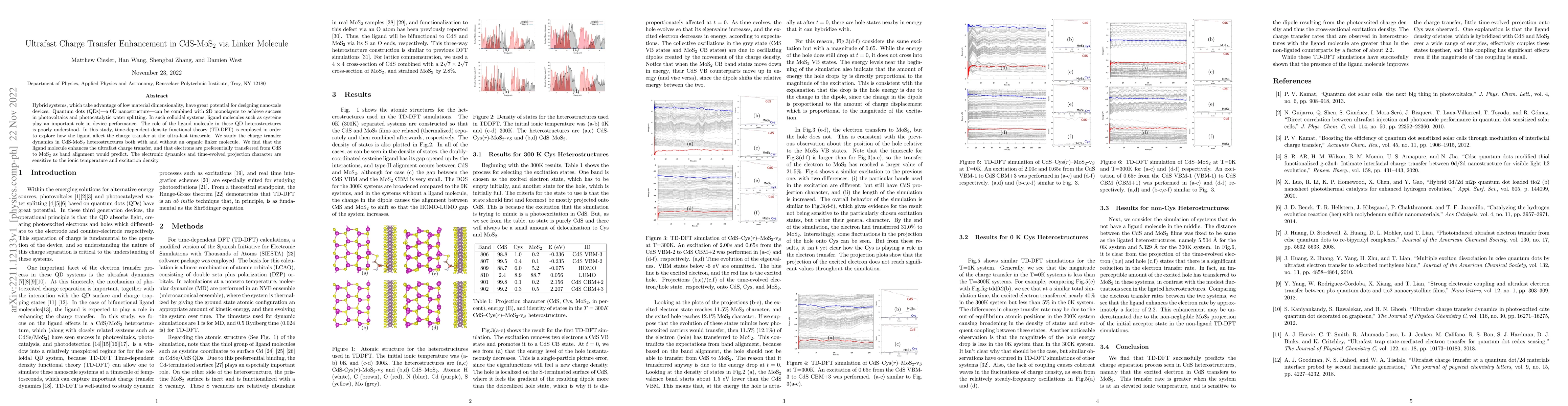
Hybrid systems, which take advantage of low material dimensionality, have great potential for designing nanoscale devices. Quantum dots (QDs) -- a 0D nanostructure -- can be combined with 2D monolay...
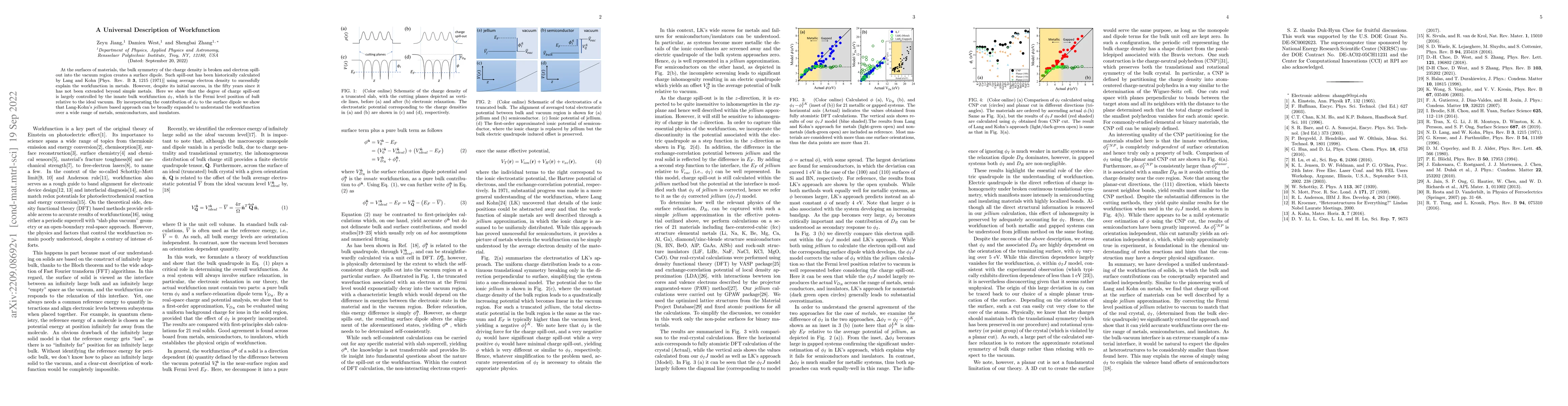
At the surfaces of materials, the bulk symmetry of the charge density is broken and electron spill-out into the vacuum region creates a surface dipole. Such spill-out has been historically calculate...
Polarons are entities of excess electrons dressed with local response of lattices, whose atomic-scale characterization is essential for understanding the many body physics arising from the electron-...
In a solid, electrons can be scattered both by phonons and other electrons. First proposed by Landau, scattering by phonons can lead to a composite entity called a polaron, in which a lattice distor...
Modern polarization theory yields surface bound charge associated with spontaneous polarization of bulk. However, understanding polarization in nano systems also requires a proper treatment of charg...
Exploring new two-dimensional (2D) van der Waals (vdW) systems is at the forefront of materials physics. Here, through molecular beam epitaxy on graphene-covered SiC(0001), we report successful grow...
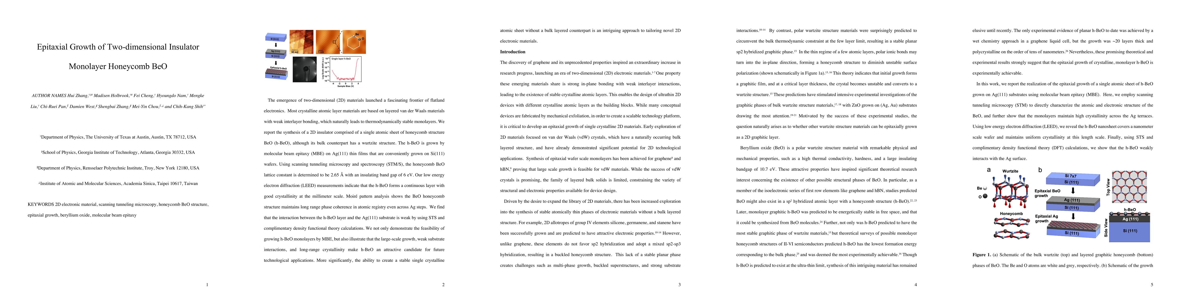
The emergence of two-dimensional (2D) materials launched a fascinating frontier of flatland electronics. Most crystalline atomic layer materials are based on layered van der Waals materials with wea...
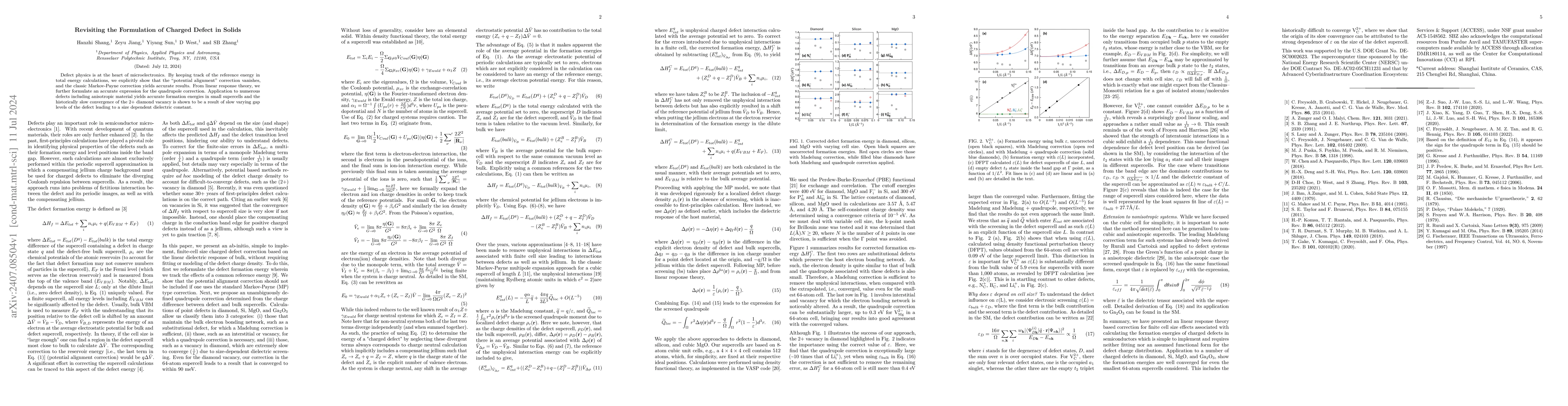
Defect physics is at the heart of microelectronics. By keeping track of the reference energy in total energy calculations, we explicitly show that the "potential alignment" correction vanishes, and th...
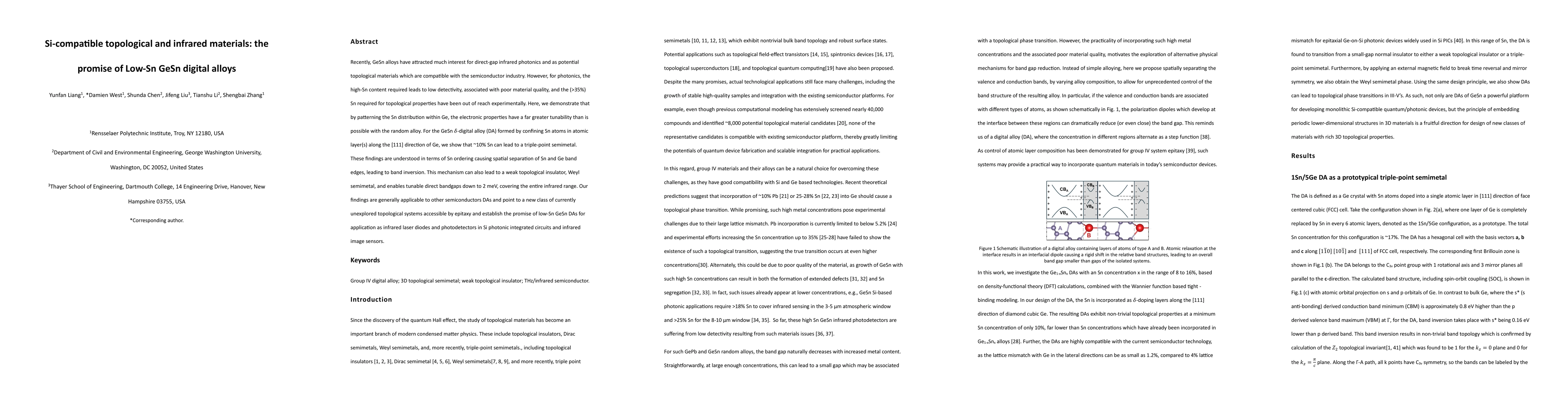
Recently, GeSn alloys have attracted much interest for direct-gap infrared photonics and as potential topological materials which are compatible with the semiconductor industry. However, for photonics...
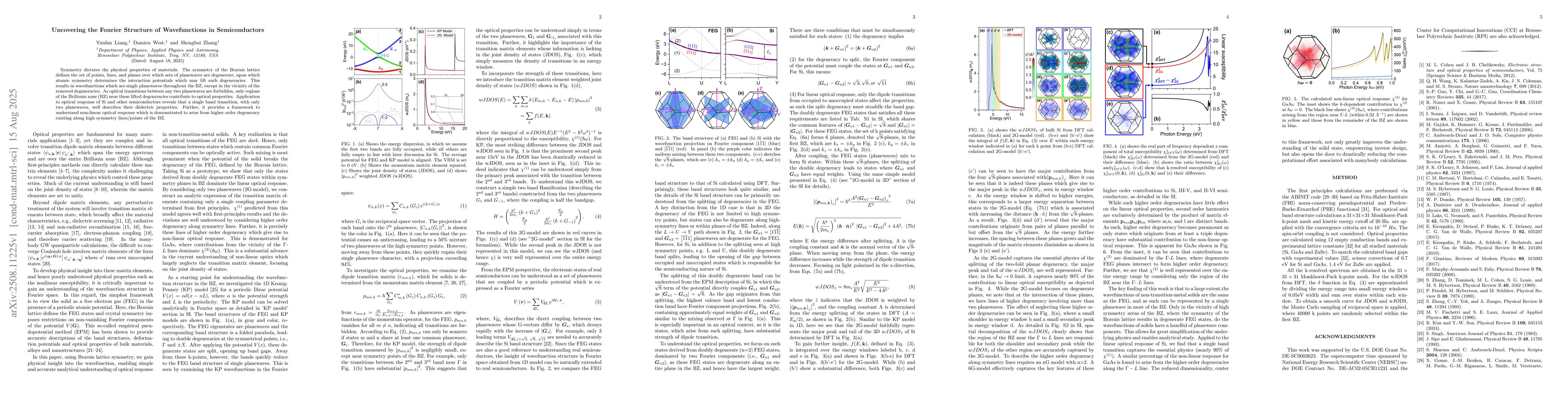
Symmetry dictates the physical properties of materials. The symmetry of the Bravais lattice defines the set of points, lines, and planes over which sets of planewaves are degenerate, upon which atomic...