Academic Profile
Statistics
Similar Authors
Papers on arXiv
Graphene is a promising material for applications as a channel in graphene field-effect transistors (GFETs) which may be used as a building block for optoelectronics, high-frequency devices and sens...
Intensive research is carried out on two-dimensional materials, in particular molybdenum disulfide, towards high-performance transistors for integrated circuits. Fabricating transistors with ohmic c...
A 200 mm processing platform for the large-scale production of graphene field-effect transistor-quantum dot (GFET-QD) hybrid photodetectors is demonstrated. Comprehensive statistical analysis of ele...
The deposition of dielectric materials on graphene is one of the bottlenecks for unlocking the potential of graphene in electronic applications. In this paper we demonstrate the plasma enhanced atom...
We demonstrate the design, fabrication, and characterization of wafer-scale, zero-bias power detectors based on two-dimensional MoS$_2$ field effect transistors (FETs). The MoS$_2$ FETs are fabricat...
PtSe$_2$ is one of the most promising materials for the next generation of piezoresistive sensors. However, the large-scale synthesis of homogeneous thin films with reproducible electromechanical pr...
Flexible energy harvesting devices fabricated in scalable thin-film processes are important components in the field of wearable electronics and the Internet of Things. We present a flexible rectenna...
Despite the enormous progress achieved during the past decade, nanoelectronic devices based on two-dimensional (2D) semiconductors still suffer from a limited electrical stability. This limited stab...
Platinum diselenide (PtSe${_2}$) is a two-dimensional (2D) material with outstanding electronic and piezoresistive properties. The material can be grown at low temperatures in a scalable manner whic...
Diodes made of heterostructures of the 2D material graphene and conventional 3D materials are reviewed in this manuscript. Several applications in high frequency electronics and optoelectronics are ...
Dominating electron-electron scattering enables viscous electron flow exhibiting hydrodynamic current density patterns such as Poiseuille profiles or vortices. The viscous regime has recently been o...
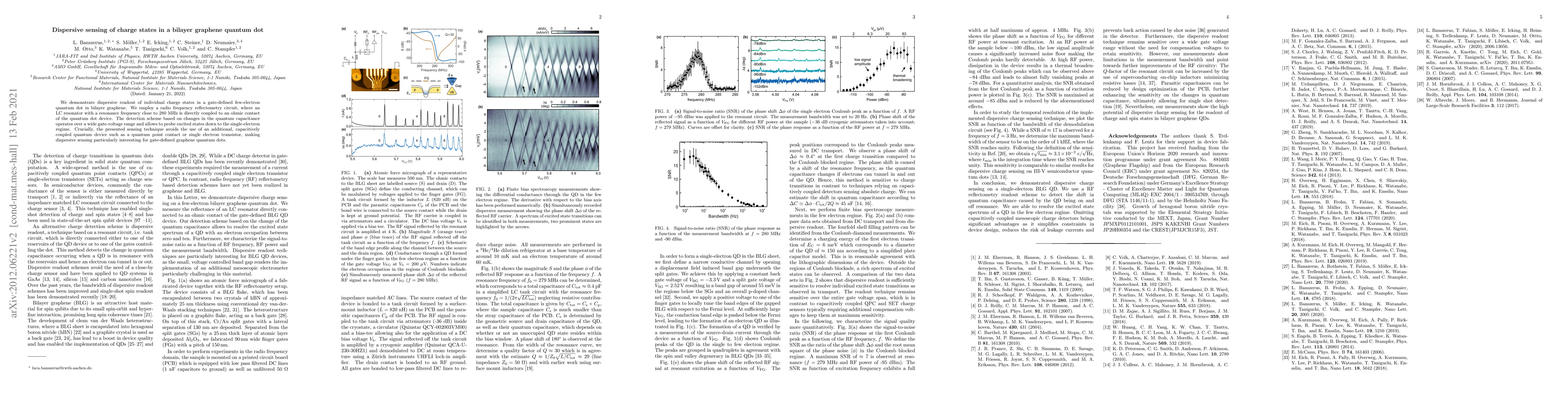
We demonstrate dispersive readout of individual charge states in a gate-defined few-electron quantum dot in bilayer graphene. We employ a radio frequency reflectometry circuit, where an LC resonator...
Hexagonal boron nitride (h-BN) is well-established as a requisite support, encapsulant and barrier for 2D material technologies, but also recently as an active material for applications ranging from...
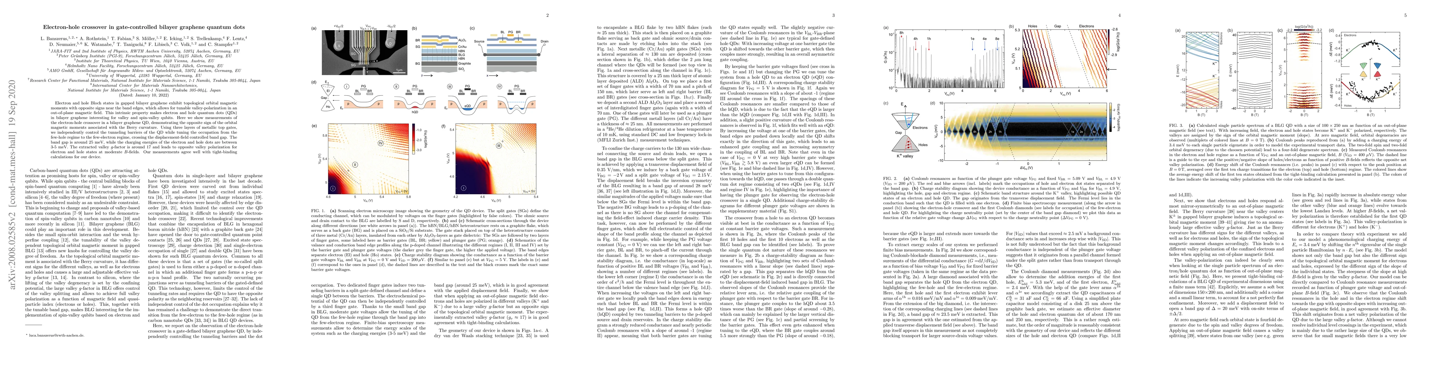
Electron and hole Bloch states in gapped bilayer graphene exhibit topological orbital magnetic moments with opposite signs near the band edges, which allows for tunable valley-polarization in an out...
In this work, a novel one-dimensional geometry for metal-insulator-graphene (1D-MIG) diode with low capacitance is demonstrated. The junction of the 1D-MIG diode is formed at the 1D edge of Al2O3-en...
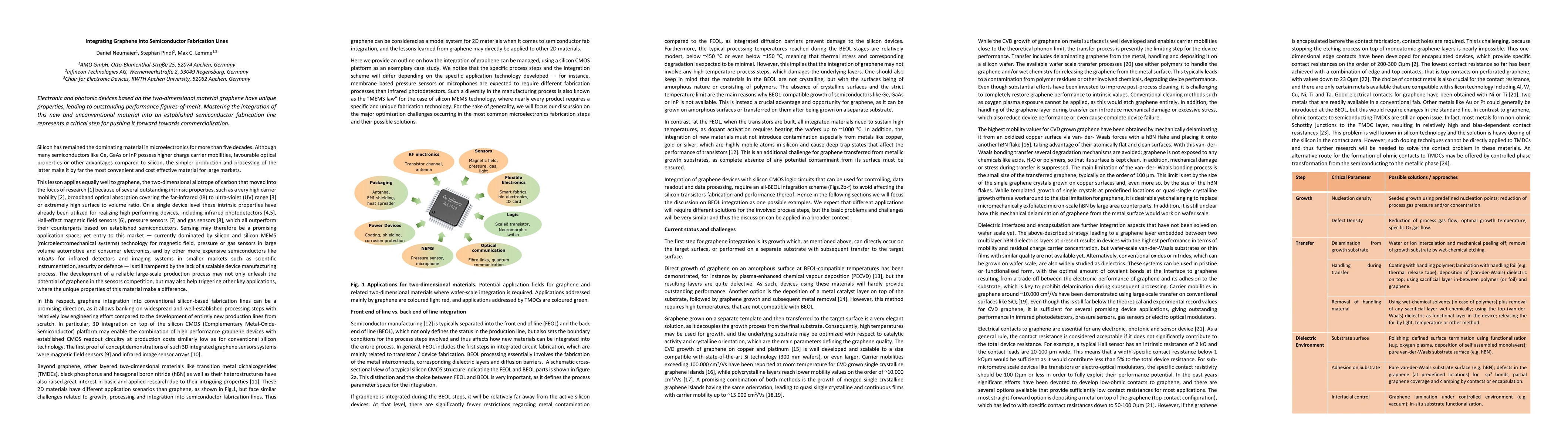
Electronic and photonic devices based on the two-dimensional material graphene have unique properties, leading to outstanding performance figures-of-merit. Mastering the integration of this new and ...
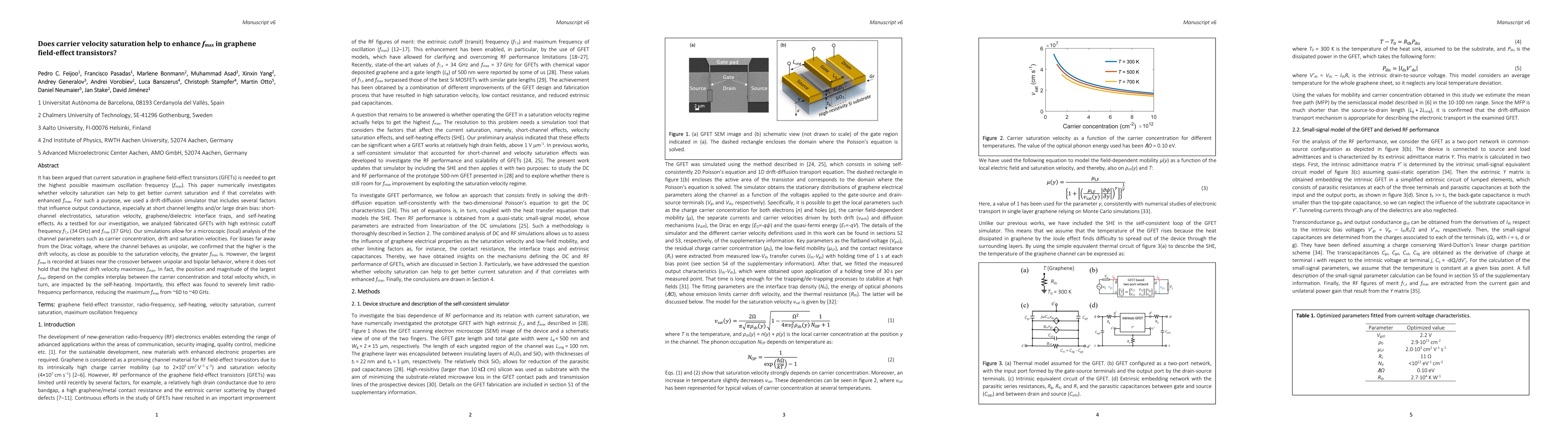
It has been argued that current saturation in graphene field-effect transistors (GFETs) is needed to get the highest possible maximum oscillation frequency (fmax). This paper numerically investigate...
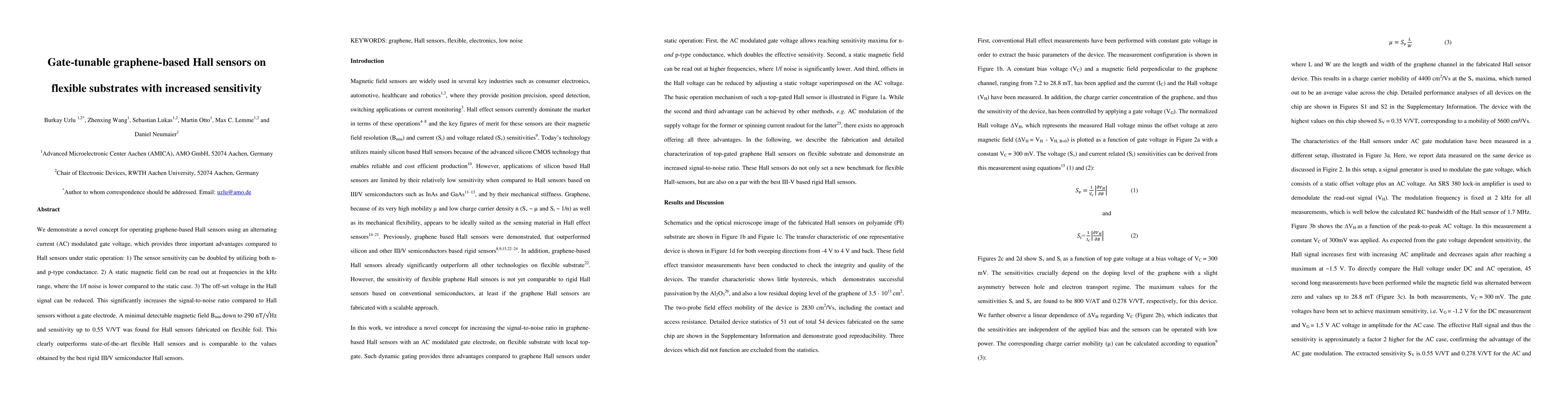
We demonstrate a novel concept for operating graphene-based Hall sensors using an alternating current (AC) modulated gate voltage, which provides three important advantages compared to Hall sensors ...
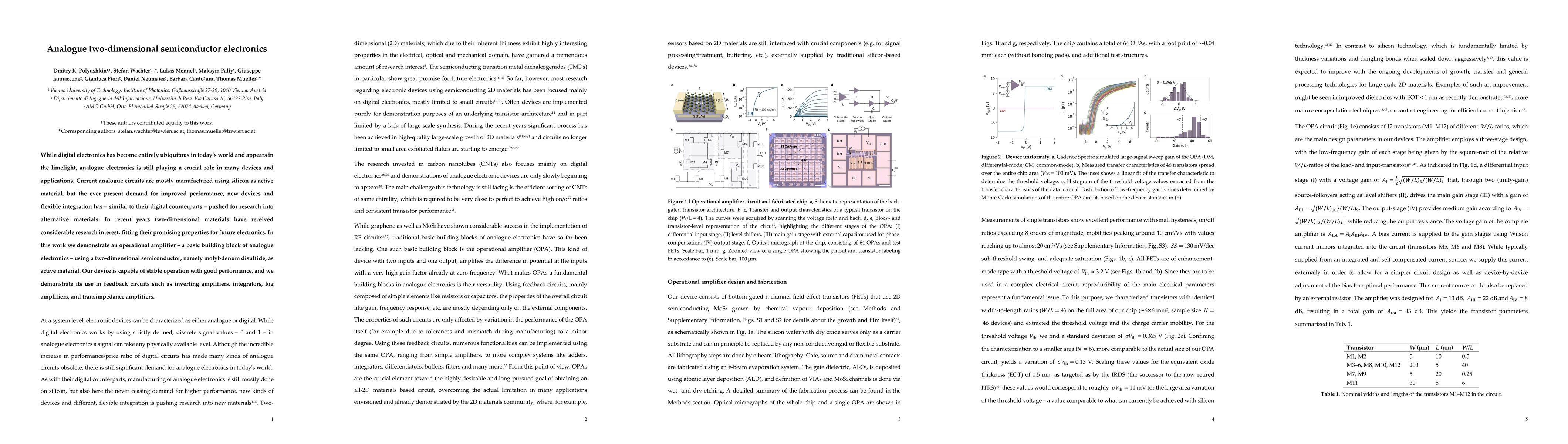
While digital electronics has become entirely ubiquitous in today's world and appears in the limelight, analogue electronics is still playing a crucial role in many devices and applications. Current...
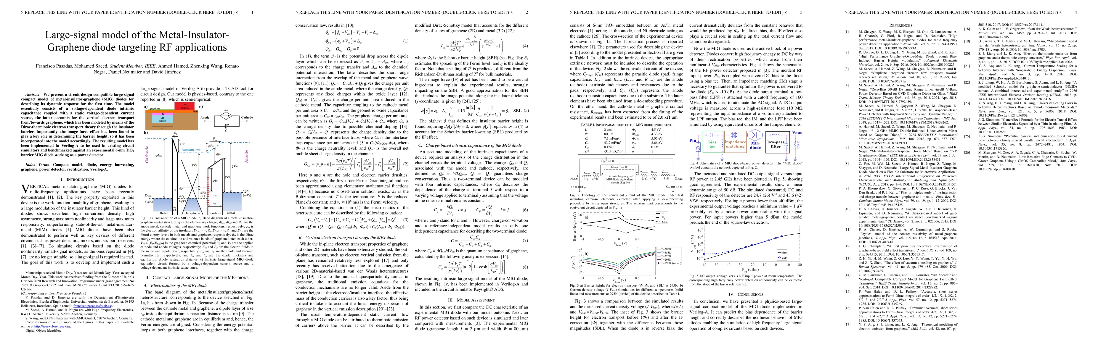
We present a circuit-design compatible large-signal compact model of metal-insulator-graphene (MIG) diodes for describing its dynamic response for the first time. The model essentially consists of a...
Two-dimensional materials (2DMs) have been widely investigated because of their potential for heterogeneous integration with modern electronics. However, several major challenges remain, such as the d...