Academic Profile
Statistics
Similar Authors
Papers on arXiv
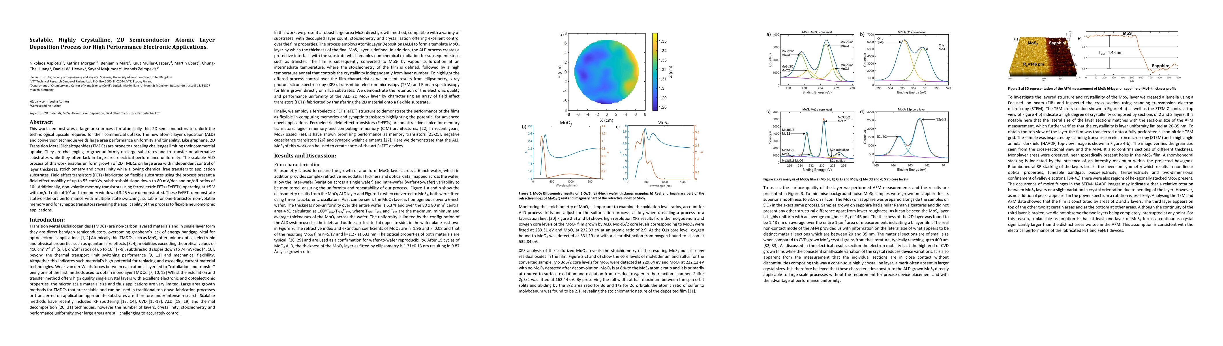
This work demonstrates a large area process for atomically thin 2D semiconductors to unlock the technological upscale required for their commercial uptake. The new atomic layer deposition (ALD) and ...
The switchable optical and electrical properties of phase change materials (PCMs) are finding new applications beyond data storage in reconfigurable photonic devices. However, high power heat pulses...
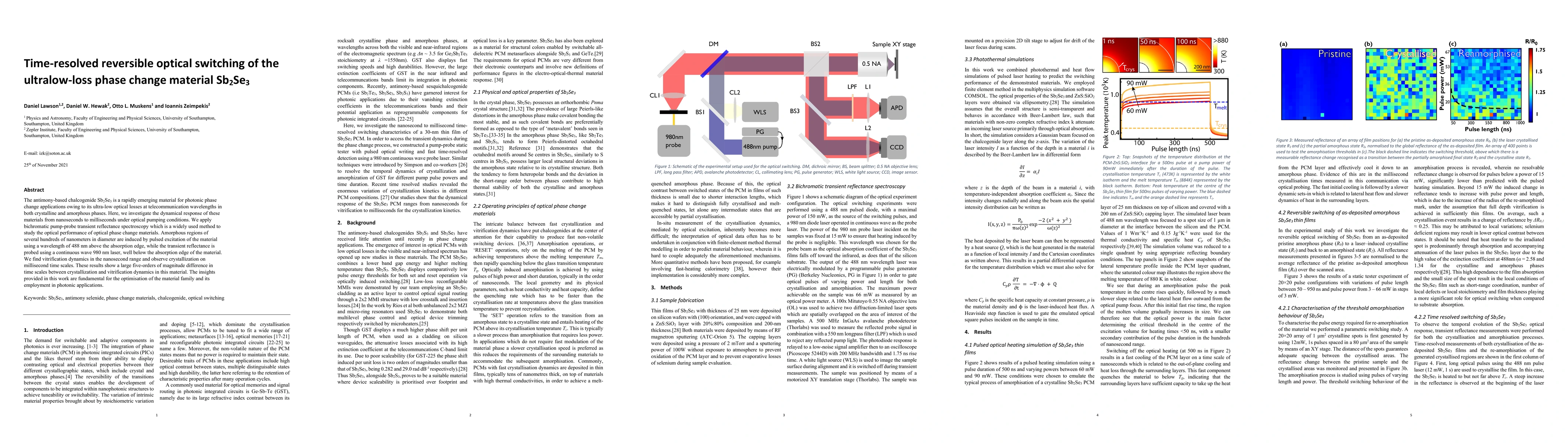
The antimony-based chalcogenide Sb2Se3 is a rapidly emerging material for photonic phase change applications owing to its ultra-low optical losses at telecommunication wavelengths in both crystallin...
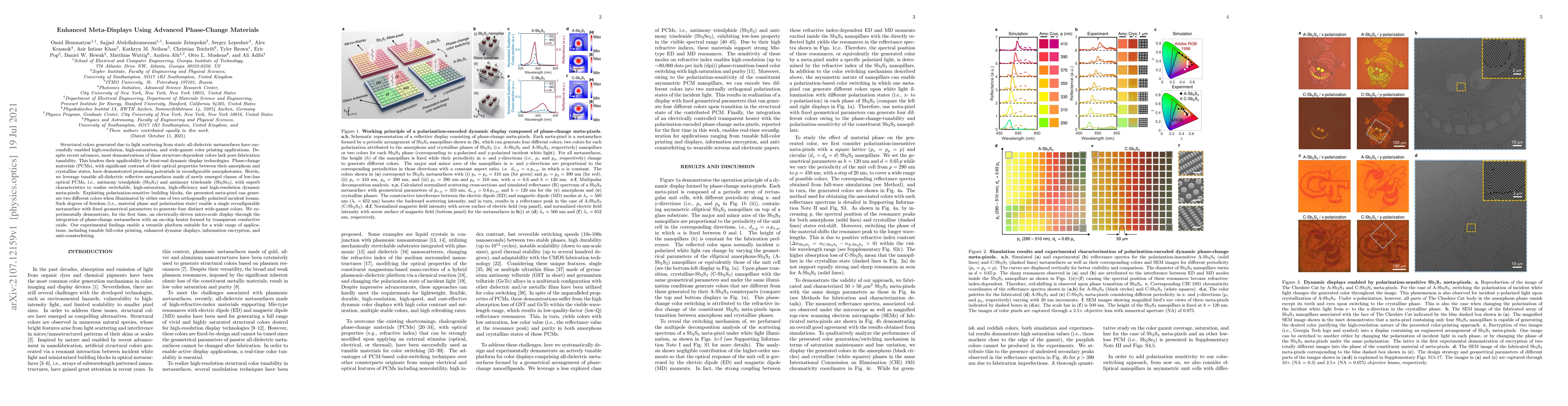
Structural colors generated due to light scattering from static all-dielectric metasurfaces have successfully enabled high-resolution, high-saturation, and wide-gamut color printing applications. De...
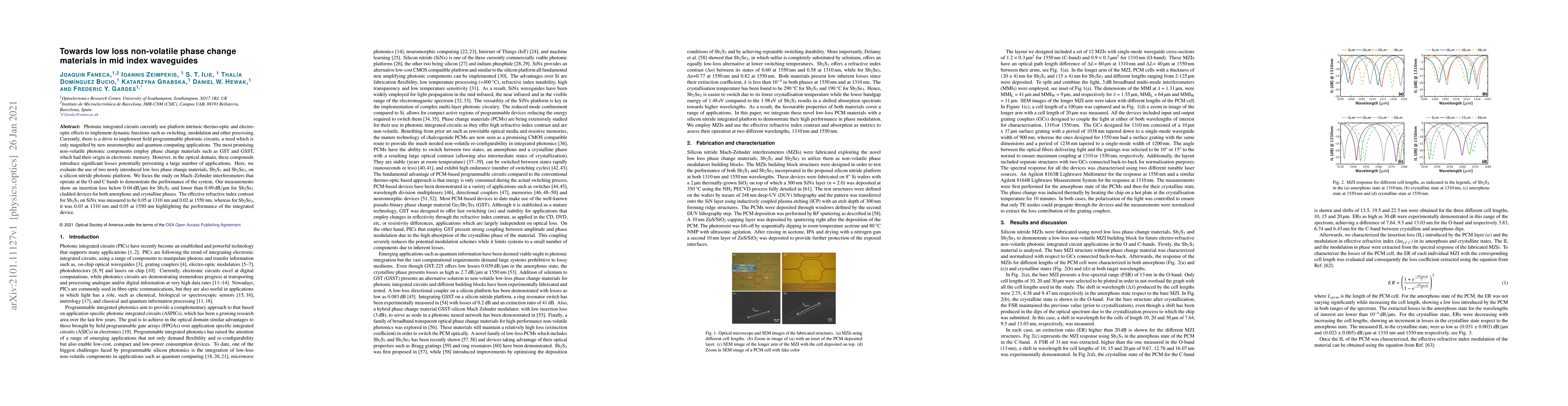
Photonic integrated circuits currently use platform intrinsic thermo-optic and electro-optic effects to implement dynamic functions such as switching, modulation and other processing. Currently, the...
Adaptable, reconfigurable and programmable are key functionalities for the next generation of silicon-based photonic processors, neural and quantum networks. Phase change technology offers proven no...