Academic Profile
Statistics
Similar Authors
Papers on arXiv
Recent studies have focused on the relationship between charge density wave (CDW) collective electronic ground states and nontrivial topological states. Using angle-resolved photoemission and densit...
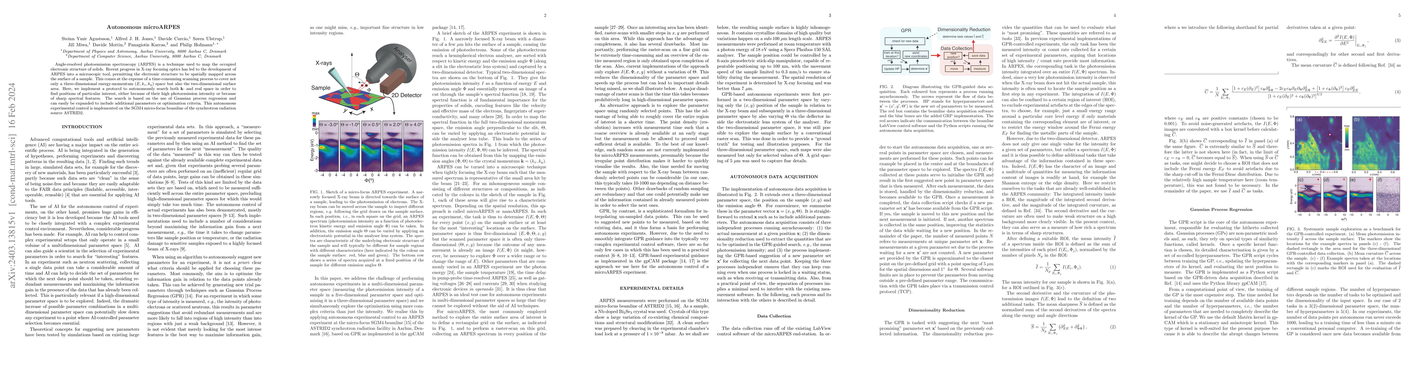
Angle-resolved photoemission spectroscopy (ARPES) is a technique used to map the occupied electronic structure of solids. Recent progress in X-ray focusing optics has led to the development of ARPES...
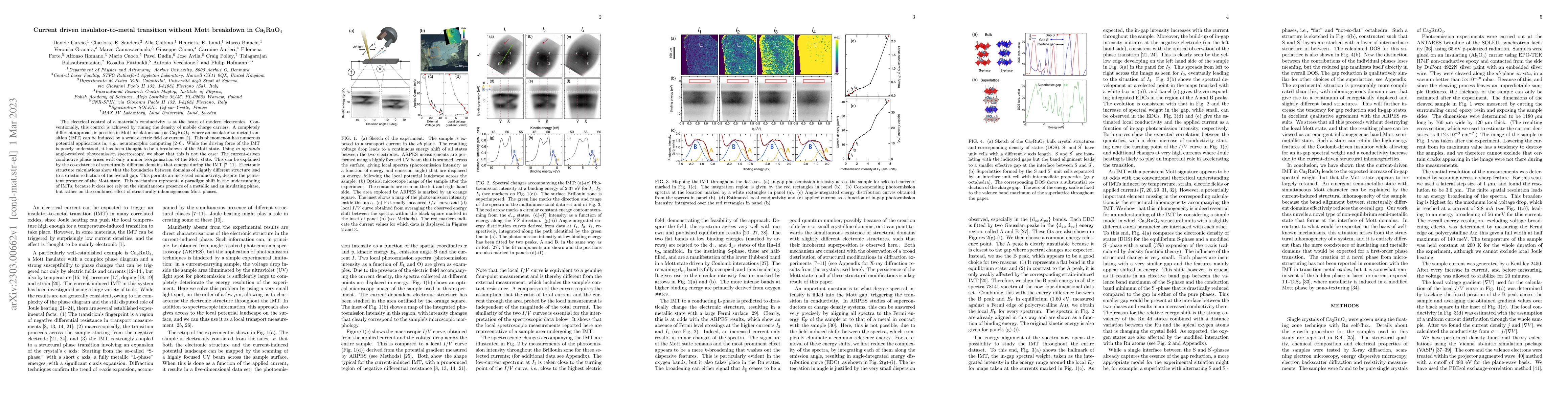
The electrical control of a material's conductivity is at the heart of modern electronics. Conventionally, this control is achieved by tuning the density of mobile charge carriers. A completely diff...
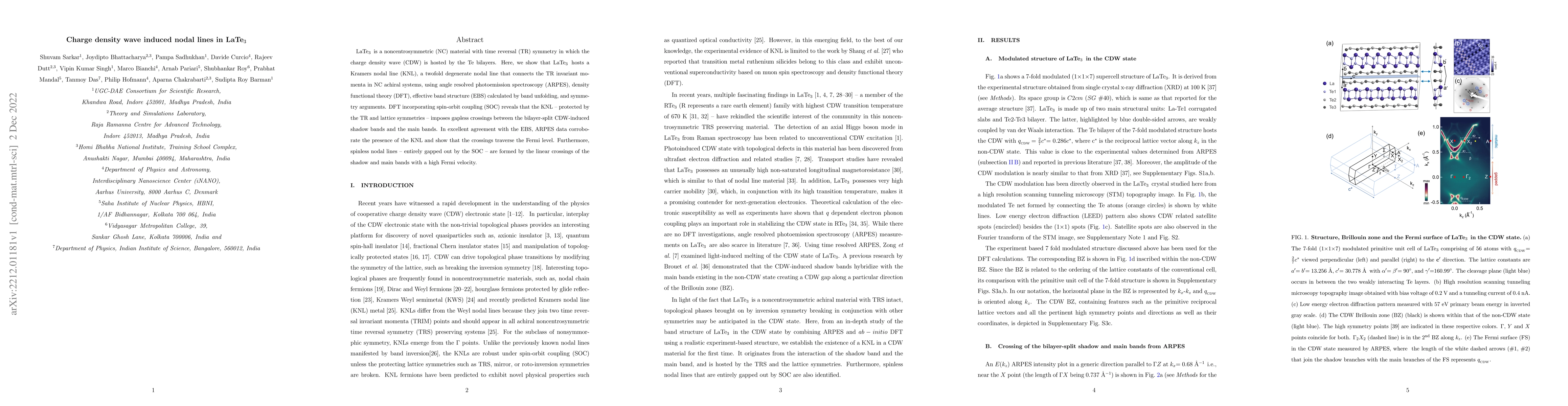
LaTe$_3$ is a noncentrosymmetric (NC) material with time reversal (TR) symmetry in which the charge density wave (CDW) is hosted by the Te bilayers. Here, we show that LaTe$_3$ hosts a Kramers nodal...
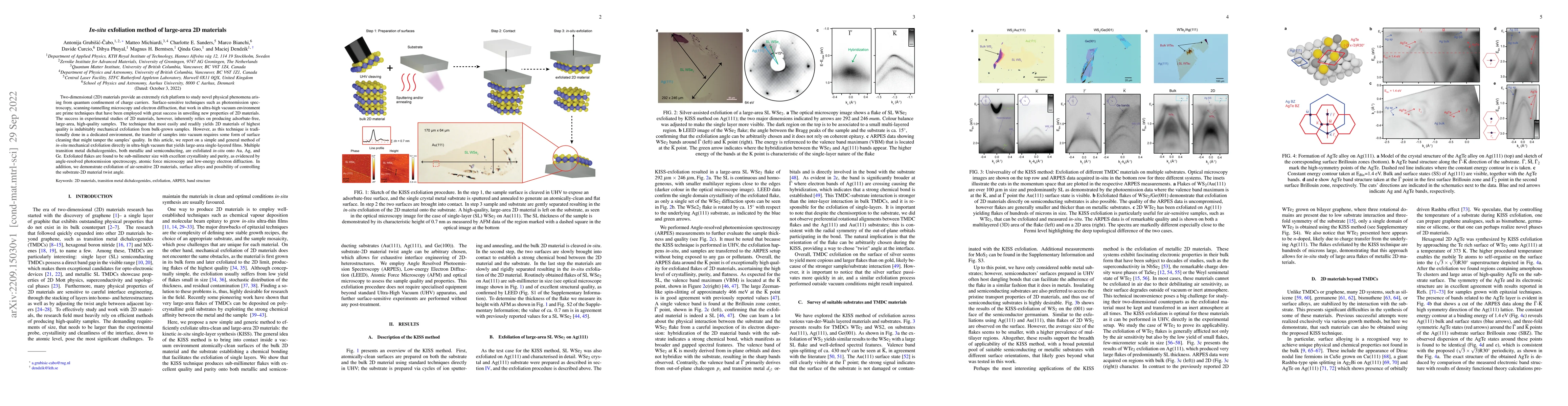
The success in studying 2D materials inherently relies on producing samples of large area, and high quality enough for the experimental conditions. Because their 2D nature surface sensitive techniqu...
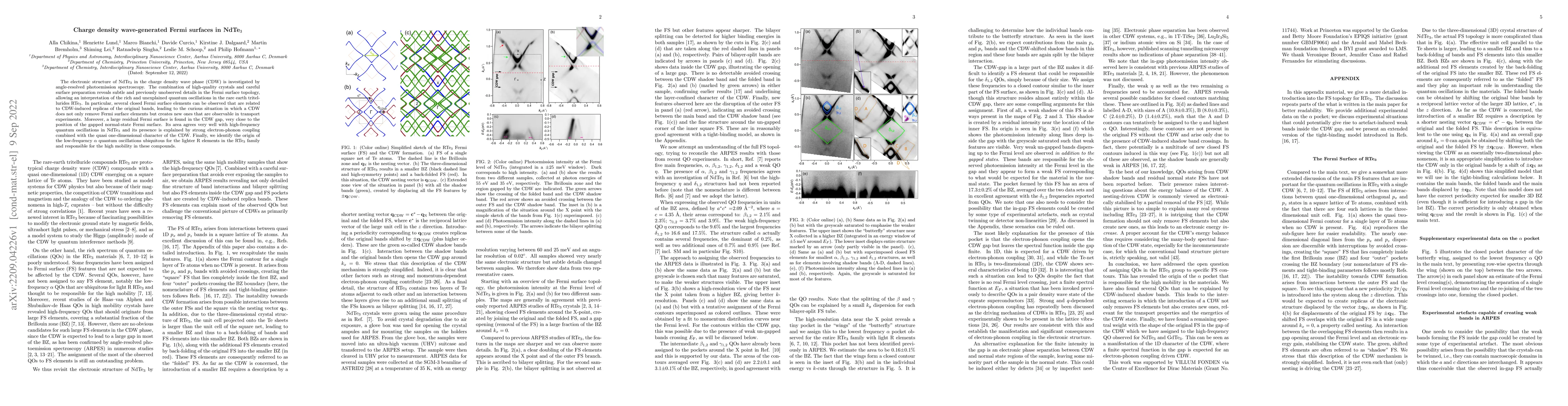
The electronic structure of NdTe$_3$ in the charge density wave phase (CDW) is investigated by angle-resolved photoemission spectroscopy. The combination of high-quality crystals and careful surface...
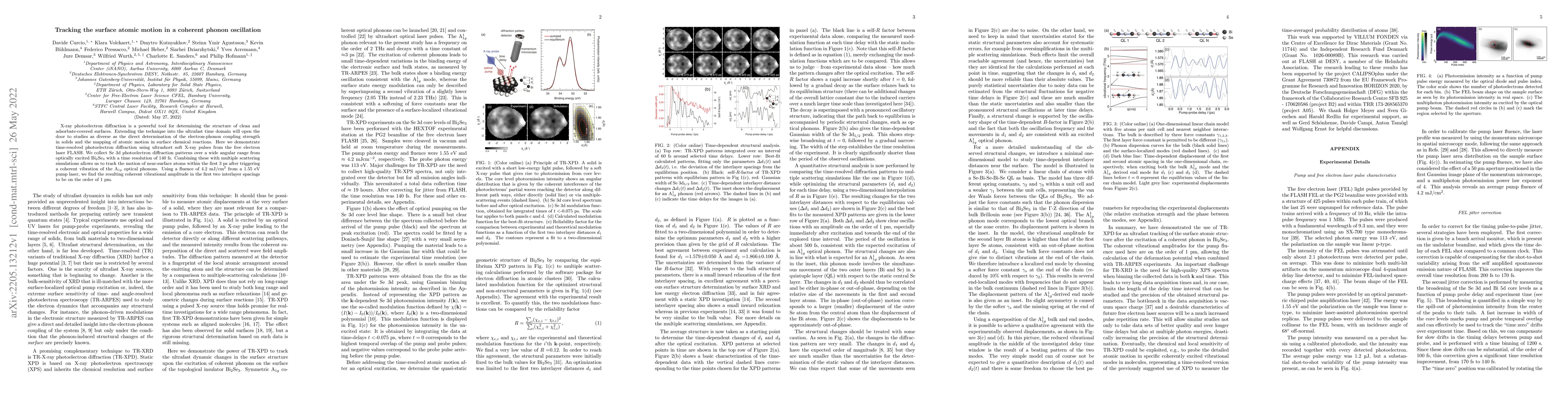
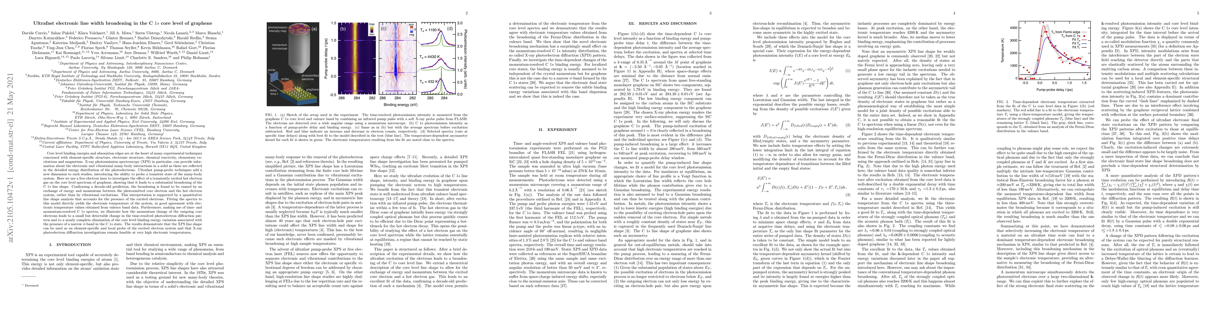
X-ray photoelectron diffraction is a powerful tool for determining the structure of clean and adsorbate-covered surfaces. Extending the technique into the ultrafast time domain will open the door to...
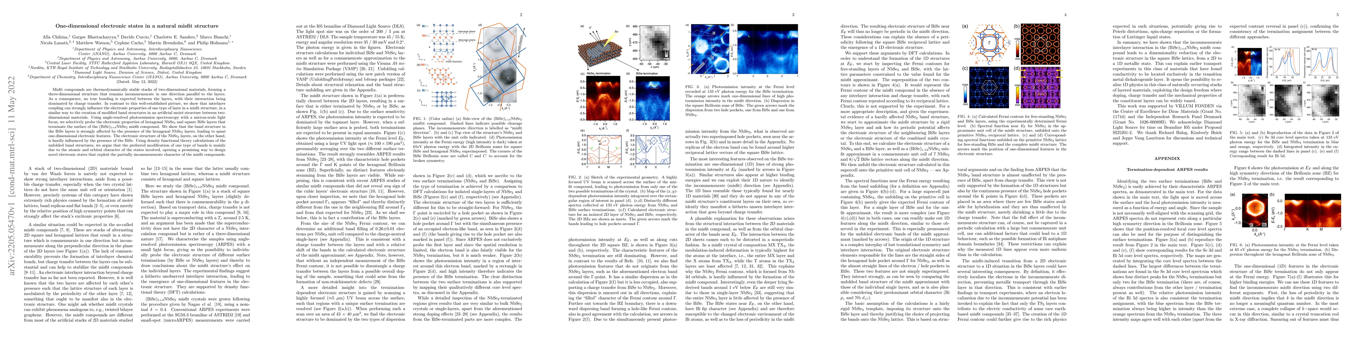
Misfit compounds are thermodynamically stable stacks of two-dimensional materials, forming a three-dimensional structure that remains incommensurate in one direction parallel to the layers. As a con...
A mismatch of atomic registries between single-layer transition metal dichalcogenides (TMDs) in a two dimensional van der Waals heterostructure produces a moir\'e superlattice with a periodic potent...
Core level binding energies and absorption edges are at the heart of many experimental techniques concerned with element-specific structure, electronic structure, chemical reactivity, elementary exc...
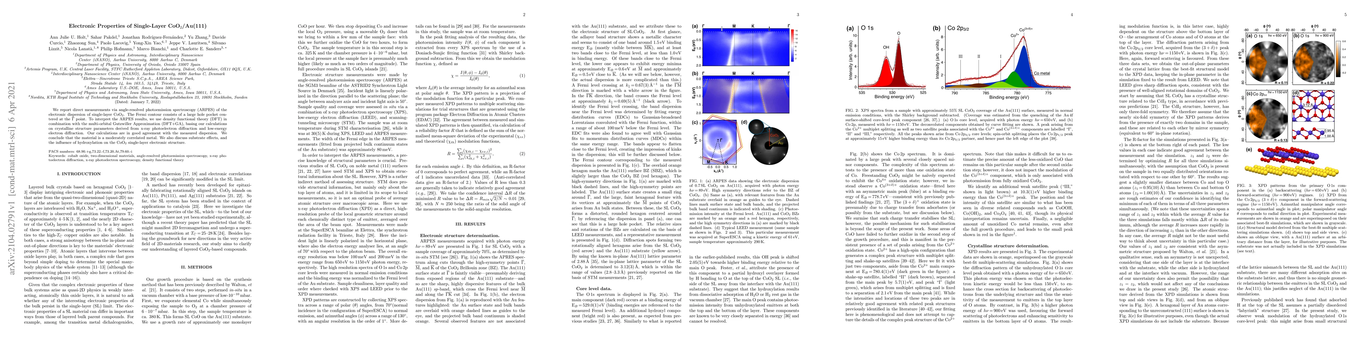
We report direct measurements via angle-resolved photoemission spectroscopy (ARPES) of the electronic dispersion of single-layer CoO$_2$. The Fermi contour consists of a large hole pocket centered a...
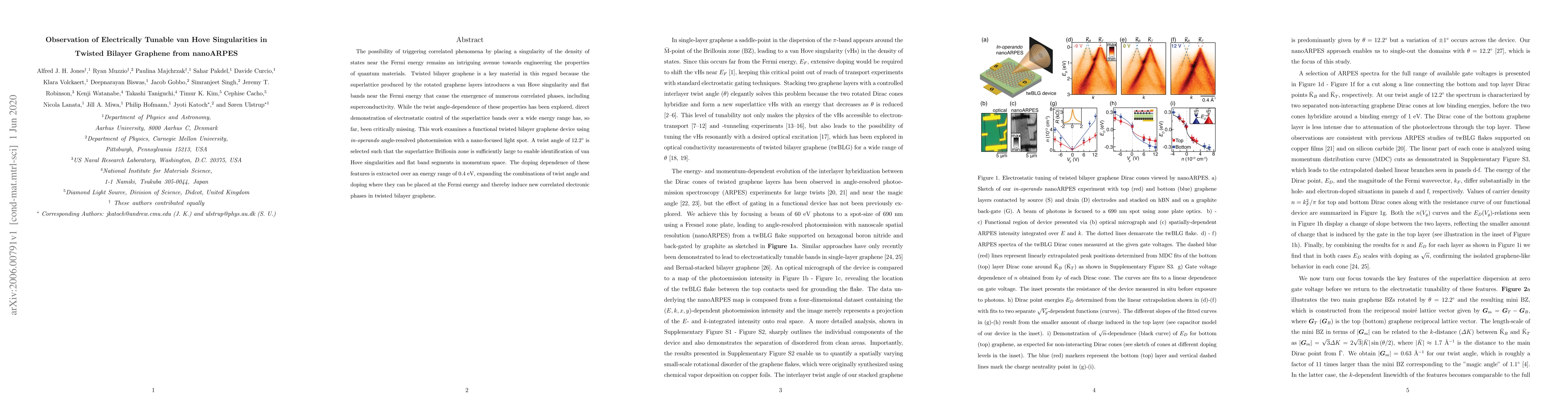
The possibility of triggering correlated phenomena by placing a singularity of the density of states near the Fermi energy remains an intriguing avenue towards engineering the properties of quantum ...
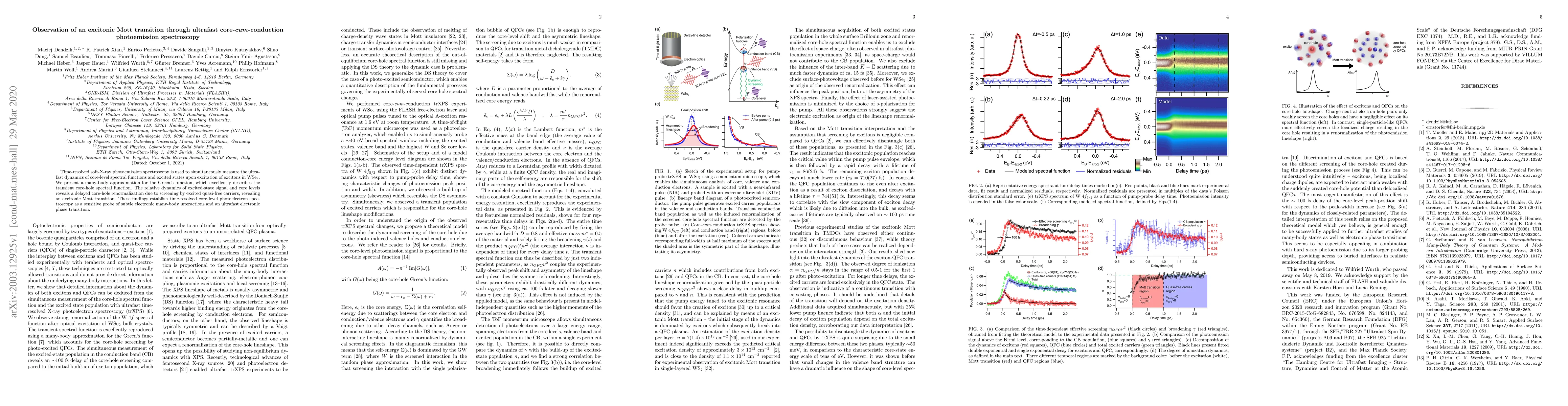
Time-resolved soft-X-ray photoemission spectroscopy is used to simultaneously measure the ultrafast dynamics of core-level spectral functions and excited states upon excitation of excitons in WSe$_2...
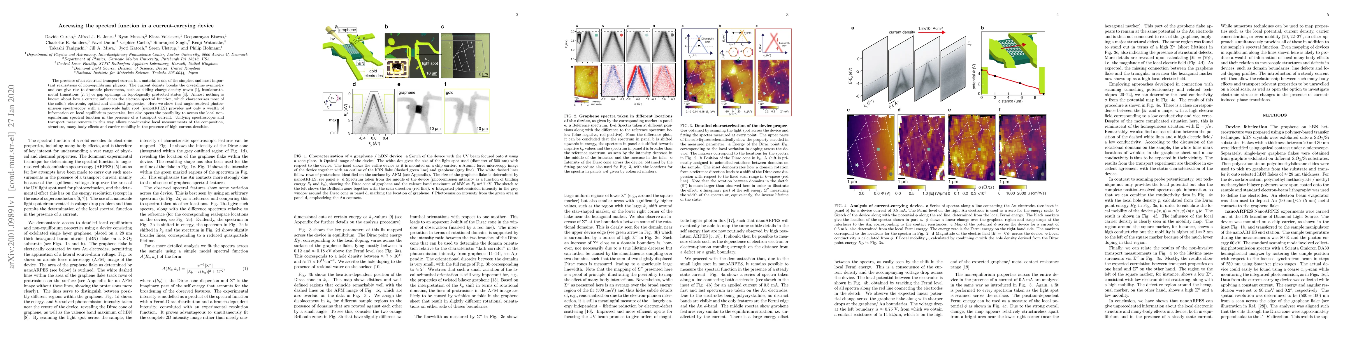
The presence of an electrical transport current in a material is one of the simplest and most important realisations of non-equilibrium physics. The current density breaks the crystalline symmetry a...
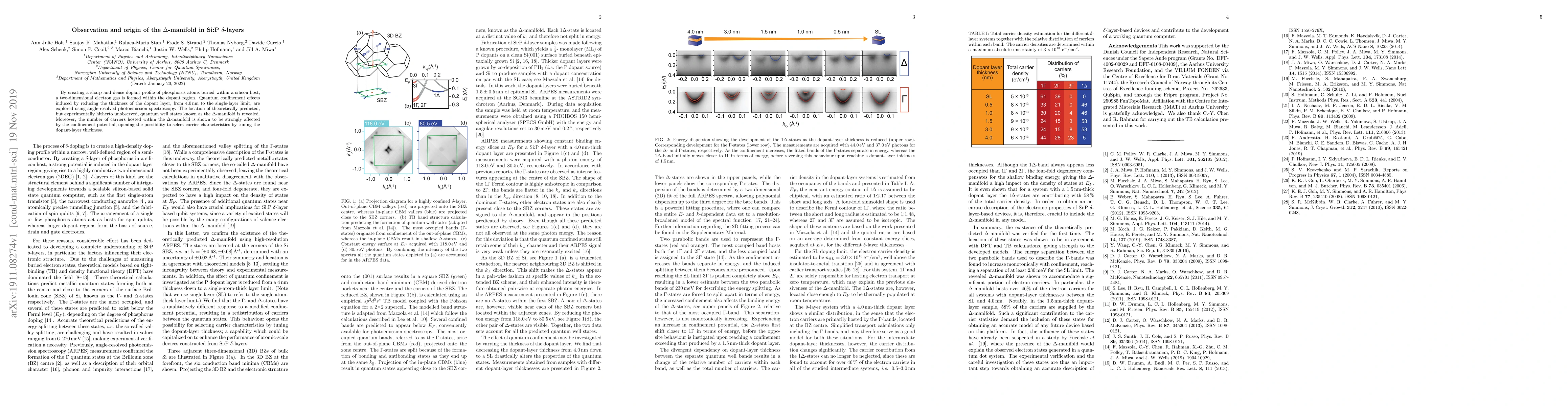
By creating a sharp and dense dopant profile of phosphorus atoms buried within a silicon host, a two-dimensional electron gas is formed within the dopant region. Quantum confinement effects induced ...
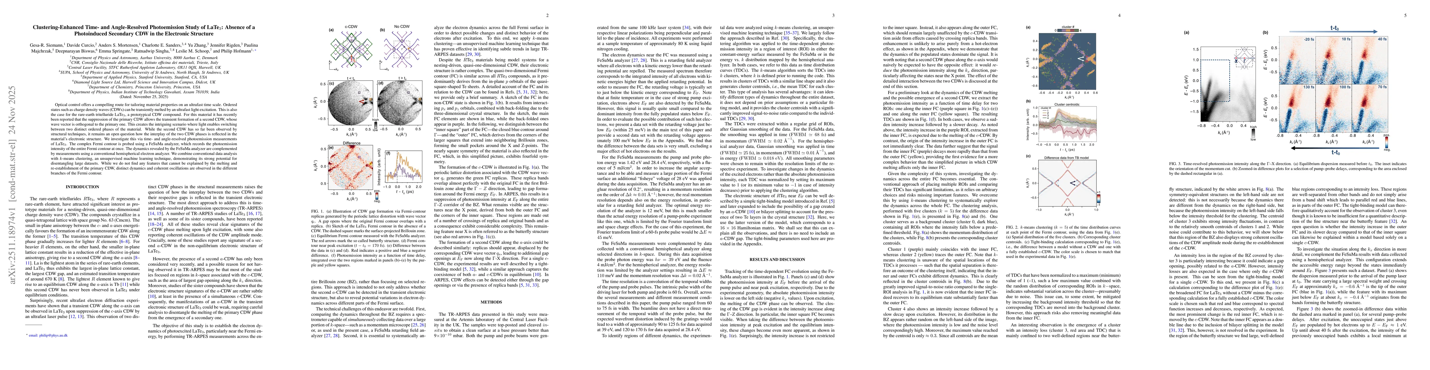
Optical control offers a compelling route for tailoring material properties on an ultrafast time scale. Ordered states such as charge density waves (CDWs) can be transiently melted by an ultrafast lig...
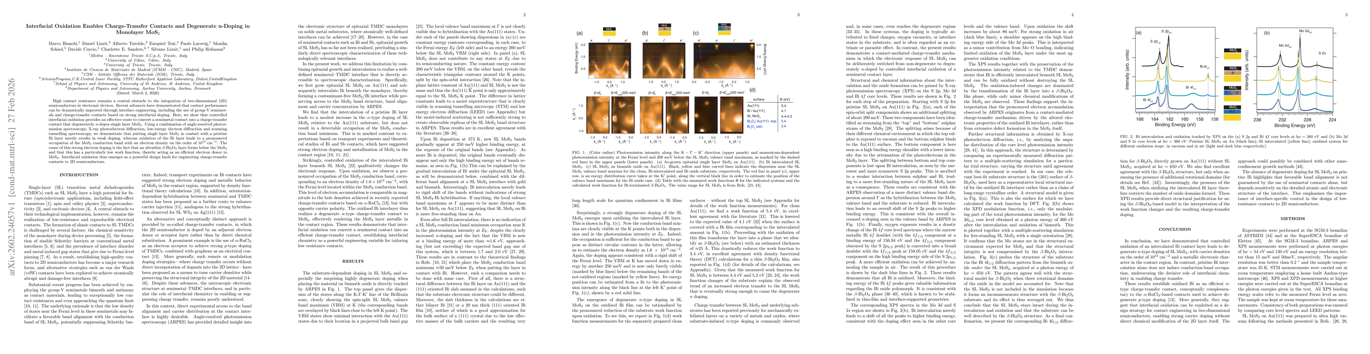
High contact resistance remains a central obstacle to the integration of two-dimensional (2D) semiconductors in electronic devices. Recent advances have demonstrated that contact performance can be dr...