ArxivLens
D
Researcher

Digbijoy N. Nath

6 papers on arXiv

6 arXiv Papers
134 Total Publications
Profile

Academic Profile

Name D. Nath
Total Papers 134
Scholar Profile View on Semantic Scholar
Metrics

Statistics

6 arXiv Papers
134 Total Publications
Publications

Papers on arXiv

Thumbnail for Laser Etch Enabled Active Embedded Microfluidic Cooling in
  $\beta$-Ga$_2$O$_3$
arXiv
Laser Etch Enabled Active Embedded Microfluidic Cooling in $\beta$-Ga$_2$O$_3$

We demonstrate active embedded microfluidic cooling in $\beta$-Ga$_2$O$_3$. We employ a cost-effective infra-red laser etch setup to achieve controlled etching of micro-channels in 500 um thick $\be...

Thumbnail for UV/Near-IR dual band photodetector based on p-GaN/{\alpha}-In2Se3
  heterojunction
arXiv
UV/Near-IR dual band photodetector based on p-GaN/{\alpha}-In2Se3 heterojunction

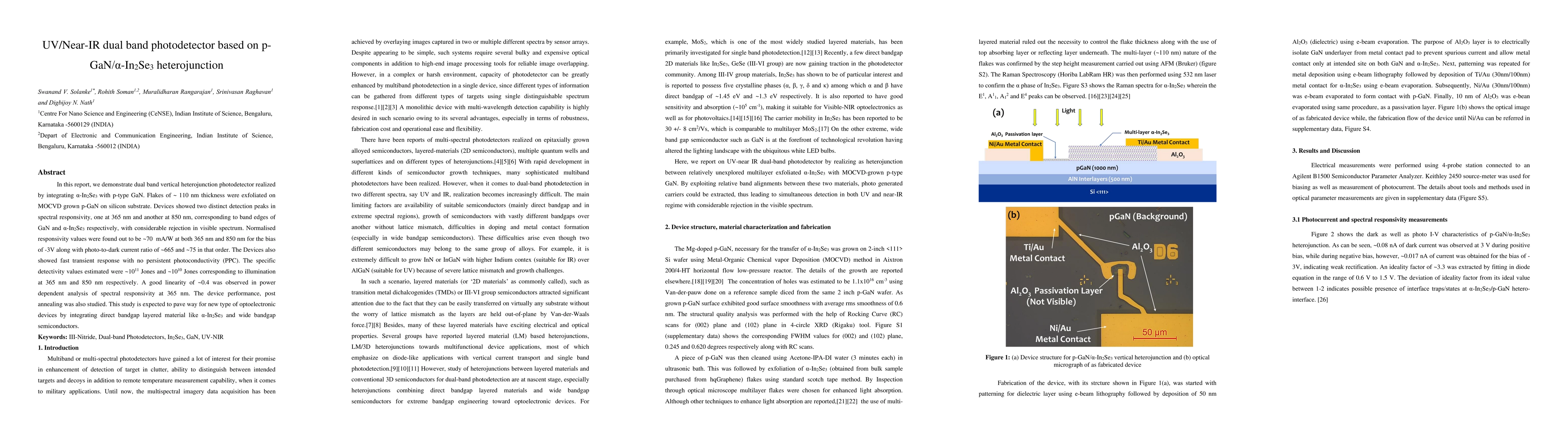
In this report, we demonstrate dual band vertical heterojunction photodetector realized by integrating {\alpha}-In2Se3 with p-type GaN. Flakes of ~ 110 nm thickness were exfoliated on MOCVD grown p-...

Thumbnail for Deep sub micron normally off AlGaN/GaN MOSFET on silicon with VTH > 5V
  and On Current > 0.5 A/mm
arXiv
Deep sub micron normally off AlGaN/GaN MOSFET on silicon with VTH > 5V and On Current > 0.5 A/mm

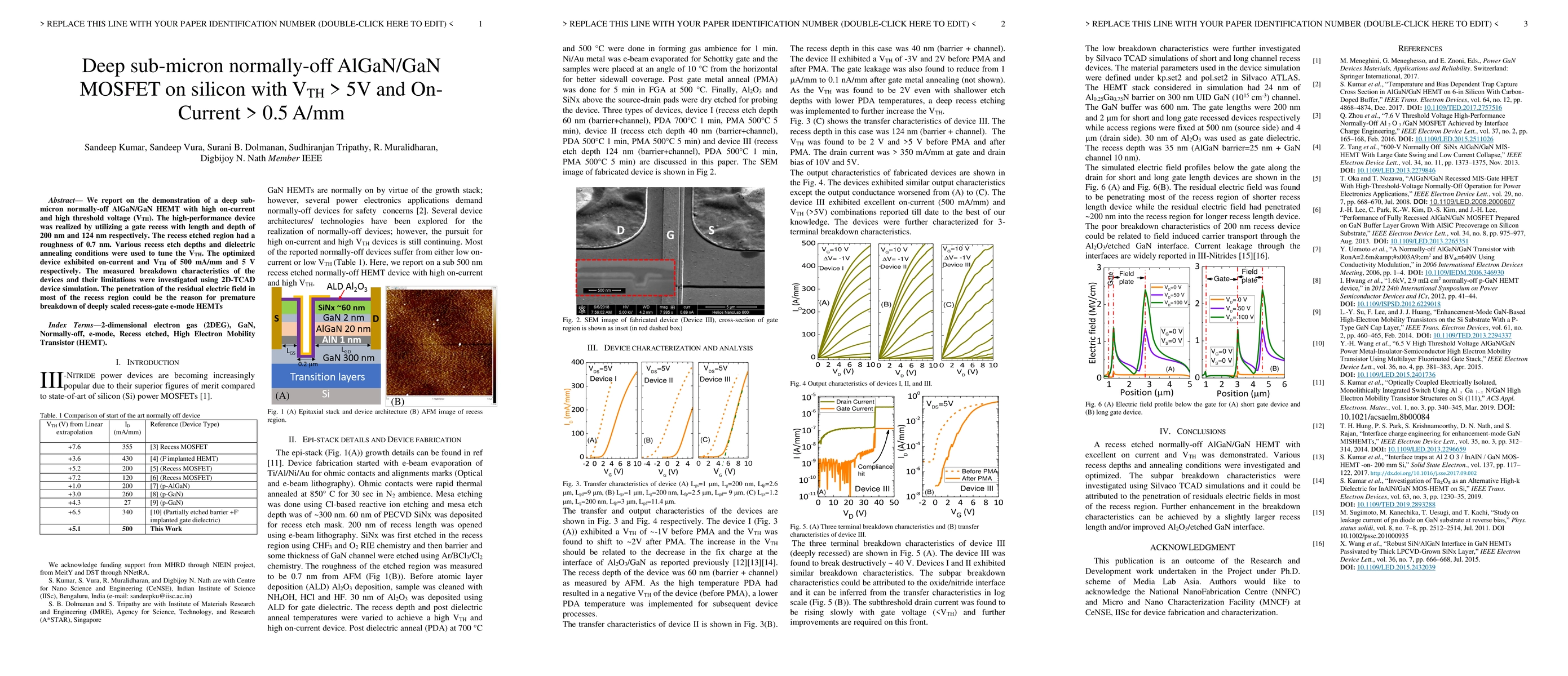
We report on the demonstration of a deep sub-micron normally-off AlGaN/GaN HEMT with high on-current and high threshold voltage (VTH). The high-performance device was realized by utilizing a gate re...

Thumbnail for Meandering gate edges for breakdown voltage enhancement in AlGaN/GaN
  HEMTs
arXiv
Meandering gate edges for breakdown voltage enhancement in AlGaN/GaN HEMTs

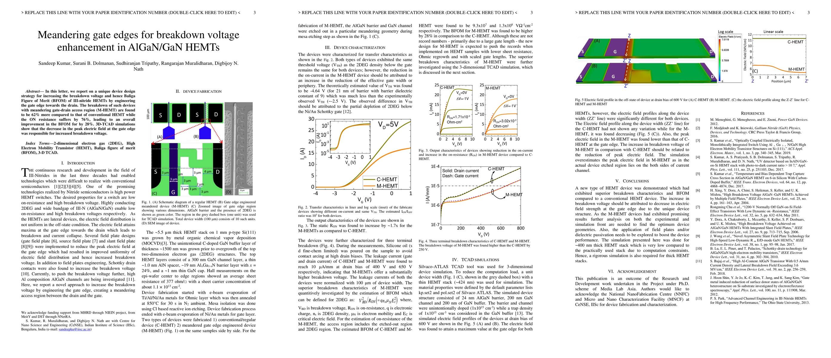
In this letter, we report on a unique device design strategy for increasing the breakdown voltage and hence Baliga Figure of Merit (BFOM) of III-nitride HEMTs by engineering the gate edge towards th...

Thumbnail for Investigation of Ta2O5 as an alternative high \k{appa} dielectric for
  InAlN/GaN MOS HEMT on Si
arXiv
Investigation of Ta2O5 as an alternative high \k{appa} dielectric for InAlN/GaN MOS HEMT on Si

We report on the demonstration and investigation of Ta2O5 as high-\k{appa} dielectric for InAlN/GaN-MOS HEMT-on-Si. Ta2O5 of thickness 24 nm and dielectric constant ~ 30 was sputter deposited on InA...

Thumbnail for A performance comparison between \b{eta}-Ga2O3 and GaN High Electron
  Mobility Transistors
arXiv
A performance comparison between \b{eta}-Ga2O3 and GaN High Electron Mobility Transistors

In this letter, we report on the quantitative estimates of various metrics of performance for \b{eta}-Ga2O3 based High Electron Mobility Transistor (HEMT) for radio frequency (RF) and power applicat...

This website uses cookies to ensure you get the best experience. Learn more