Dilip K. Singh

6 papers on arXiv

Academic Profile

Name: D. Singh
Total Papers: 13

Statistics

arXiv Papers 6
Total Publications 13

Papers on arXiv

Thumbnail for Piezo-resistive pressure sensor based on CVD-grown ZnO nanowires on
  Polyethylene Tetrathalate substrate

Piezo-resistive pressure sensor based on CVD-grown ZnO nanowires on Polyethylene Tetrathalate substrate

Recent developments in the domain of electronic materials and devices have attracted the interest of researchers toward flexible and printable electronic components like organic transistors, printab...

Thumbnail for High-Efficiency Photodetector Based On CVD-Grown WS$_2$ Monolayer

High-Efficiency Photodetector Based On CVD-Grown WS$_2$ Monolayer

Future generation technologies demand high efficiency photodetectors to enable sensing and switching devices for ultrafast communication and machine vision. This require direct-band gap materials wi...

Thumbnail for Kinetics and Parameters of Epitaxial Monolayered Continuous large area
  Molybdenum disulfide Growth

Kinetics and Parameters of Epitaxial Monolayered Continuous large area Molybdenum disulfide Growth

The growth of large crystallite continuous monolayer materials like molybdenum disulfide (MoS$_2$) with desired morphology via chemical vapor deposition (CVD) remains a challenge. In CVD, the comple...

Thumbnail for Single step synthesis of size-controlled carbon quantum dots using
  electrochemical etching of graphite

Single step synthesis of size-controlled carbon quantum dots using electrochemical etching of graphite

Carbon Quantum dots (CQD's) are nanoscale sp2 hybridized carbon particles. In this work, we present a simple one-step synthesis of CQDs from the electrochemical shredding method and technique to con...

Thumbnail for Fabrication of Tungsten nanoprobes by Electrochemical etching: Role of
  cathode geometry and their use as electrical probe

Fabrication of Tungsten nanoprobes by Electrochemical etching: Role of cathode geometry and their use as electrical probe

Electrical measurement of nano-scale devices and structures requires skills and hardware to make nano-contacts. Such measurements have been difficult for number of laboratories due to cost of probe ...

Thumbnail for Carbon Nitride: Physical properties and Applications

Carbon Nitride: Physical properties and Applications

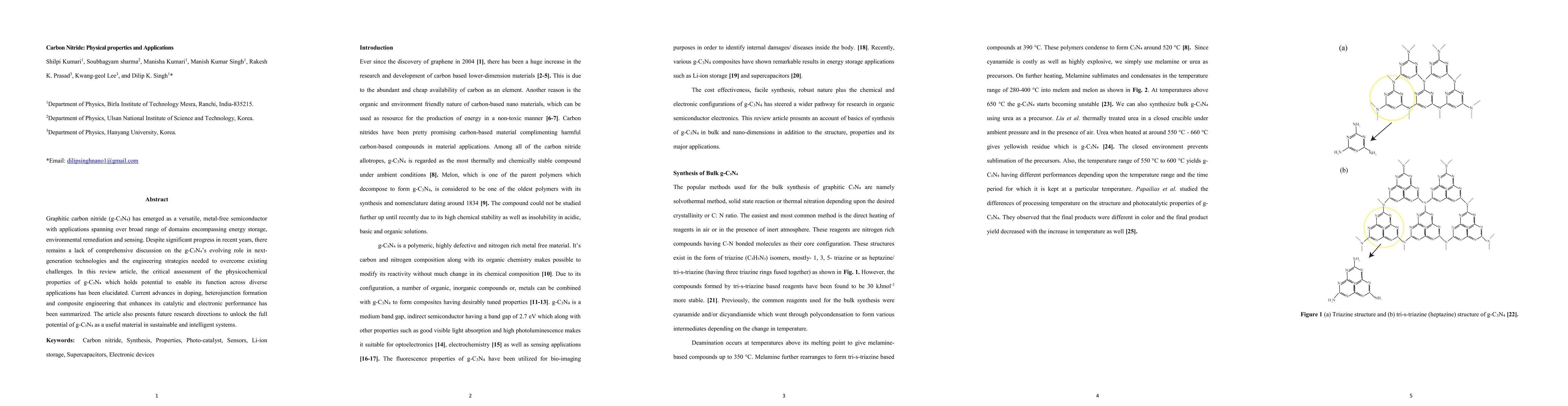
Graphitic carbon nitride has emerged as a versatile, metal-free semiconductor with applications spanning over broad range of domains encompassing energy storage, environmental remediation and sensing....

This website uses cookies to ensure you get the best experience. Learn more