ArxivLens
E
Researcher

E. Calleja

9 papers on arXiv

9 arXiv Papers
9 Total Publications
Profile

Academic Profile

Name E. Calleja
Total Papers 9
Scholar Profile View on Semantic Scholar
Metrics

Statistics

9 arXiv Papers
9 Total Publications
Publications

Papers on arXiv

Thumbnail for Photoluminescence enhancement in quaternary III-nitrides alloys grown by
  molecular beam epitaxy with increasing Al content
arXiv
Photoluminescence enhancement in quaternary III-nitrides alloys grown by molecular beam epitaxy with increasing Al content

Room temperature photoluminescence and optical absorption spectra have been measured in wurtzite In$_{x}$Al$_{y}$Ga$_{1-x-y}$N (x $\approx$ 0.06, 0.02 < y < 0.27) layers grown by molecular beam epit...

Thumbnail for Effect of the growth temperature and the AlN mole fraction on In
  incorporation and properties of quaternary III-nitride layers grown by
  molecular beam epitaxy
arXiv
Effect of the growth temperature and the AlN mole fraction on In incorporation and properties of quaternary III-nitride layers grown by molecular beam epitaxy

Indium incorporation into wurtzite (0001)-oriented In$_{x}$Al$_{y}$Ga$_{1-x-y}$N layers grown by plasma-assisted molecular beam epitaxy was studied as a function of the growth temperature (565-635 $...

Thumbnail for Formation mechanisms of single-crystalline InN quantum dots fabricated
  via droplet epitaxy
arXiv
Formation mechanisms of single-crystalline InN quantum dots fabricated via droplet epitaxy

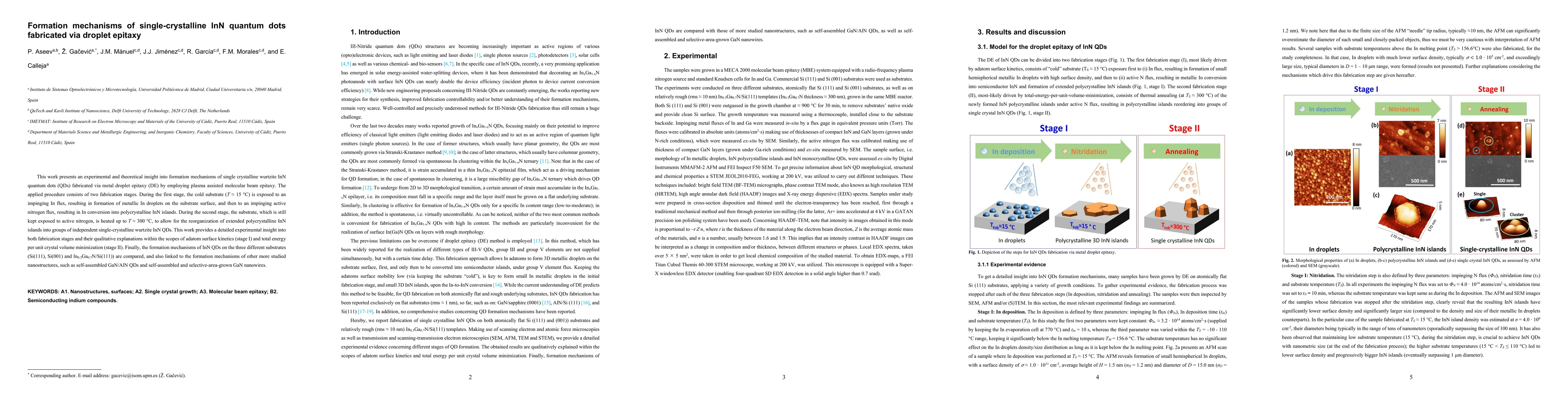
This work presents an experimental and theoretical insight into formation mechanisms of single crystalline wurtzite InN quantum dots (QDs) fabricated via metal droplet epitaxy (DE) by employing plas...

Thumbnail for Unravelling the polarity of InN quantum dots using a modified approach
  of negative-spherical-aberration imaging
arXiv
Unravelling the polarity of InN quantum dots using a modified approach of negative-spherical-aberration imaging

InN quantum dots (QDs) are considered to be promising nanostructures for different device applications. For any hexagonal AB stacking semiconductor system, polarity is an important feature which aff...

Thumbnail for In situ investigation of growth modes during plasma-assisted molecular
  beam epitaxy of (0001)GaN
arXiv
In situ investigation of growth modes during plasma-assisted molecular beam epitaxy of (0001)GaN

Real-time analysis of the growth modes during homoepitaxial (0001)GaN growth by plasma-assisted molecular beam epitaxy was performed using reflection high energy electron diffraction. A growth mode ...

Thumbnail for A comprehensive diagram to grow InAlN alloys by plasma-assisted
  molecular beam epitaxy
arXiv
A comprehensive diagram to grow InAlN alloys by plasma-assisted molecular beam epitaxy

Indium incorporation and surface morphology of InAlN layers grown on (0001)GaN by plasma-assisted molecular beam epitaxy were investigated as a function of the impinging In flux and the substrate te...

Thumbnail for In situ GaN decomposition analysis by quadrupole mass spectrometry and
  reflection high-energy electron diffraction
arXiv
In situ GaN decomposition analysis by quadrupole mass spectrometry and reflection high-energy electron diffraction

Thermal decomposition of wurtzite (0001)-oriented GaN was analyzed: in vacuum, under active N exposure, and during growth by rf-plasma assisted molecular beam epitaxy. The GaN decomposition rate was...

Thumbnail for A growth diagram for plasma-assisted molecular beam epitaxy of GaN
  nanocolumns on Si(111)
arXiv
A growth diagram for plasma-assisted molecular beam epitaxy of GaN nanocolumns on Si(111)

The morphology of GaN samples grown by plasma-assisted molecular beam epitaxy on Si(111) was systematically studied as a function of impinging Ga/N flux ratio and growth temperature (750-850{\deg}C)...

Thumbnail for Effect of different buffer layers on the quality of InGaN layers grown
  on Si
arXiv
Effect of different buffer layers on the quality of InGaN layers grown on Si

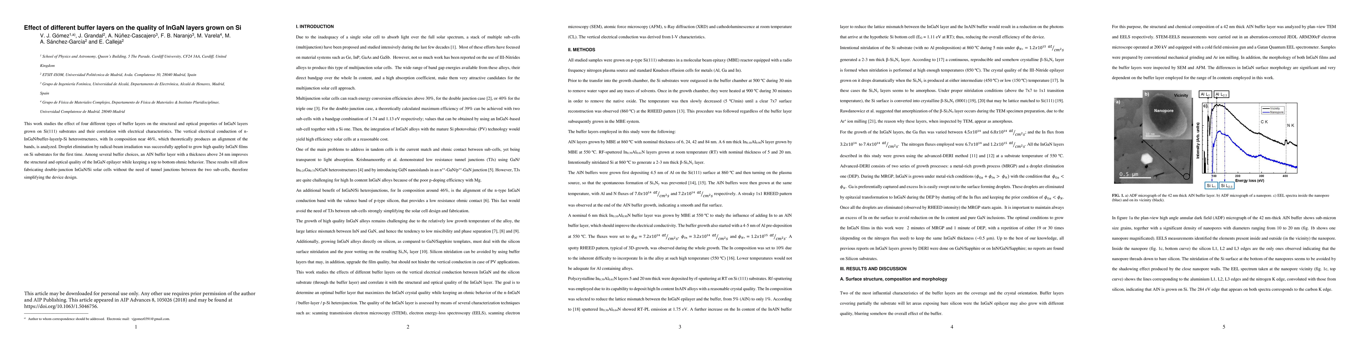
This work studies the effect of four different types of buffer layers on the structural and optical properties of InGaN layers grown on Si(111) substrates and their correlation with electrical chara...

This website uses cookies to ensure you get the best experience. Learn more