Enrique G. Marin

8 papers on arXiv

Academic Profile

Name: Enrique G. Marín
Total Papers: 5

Statistics

arXiv Papers 8
Total Publications 5

Papers on arXiv

Thumbnail for Exploiting ambipolarity in graphene field-effect transistors for novel
  designs on high-frequency analog electronics

Exploiting ambipolarity in graphene field-effect transistors for novel designs on high-frequency analog electronics

Exploiting ambipolar electrical conductivity based on graphene field-effect transistors has raised enormous interest for high-frequency (HF) analog electronics. Controlling the device polarity, by b...

Thumbnail for CVD Graphene Contacts for Lateral Heterostructure MoS${_2}$ Field Effect
  Transistors

CVD Graphene Contacts for Lateral Heterostructure MoS${_2}$ Field Effect Transistors

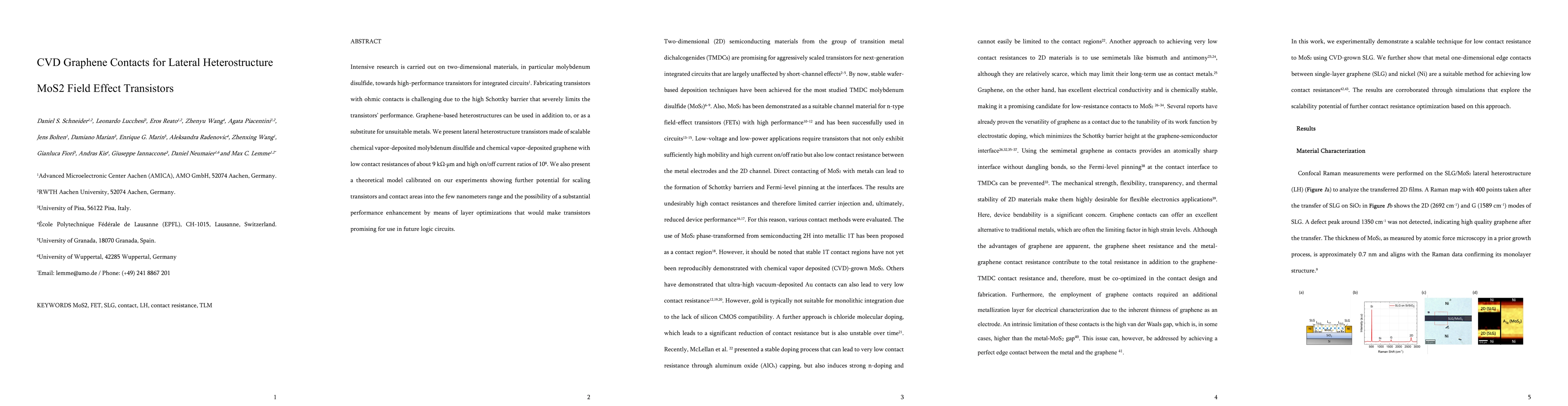
Intensive research is carried out on two-dimensional materials, in particular molybdenum disulfide, towards high-performance transistors for integrated circuits. Fabricating transistors with ohmic c...

Thumbnail for Compact Modeling of pH-Sensitive FETs Based on Two-Dimensional
  Semiconductors

Compact Modeling of pH-Sensitive FETs Based on Two-Dimensional Semiconductors

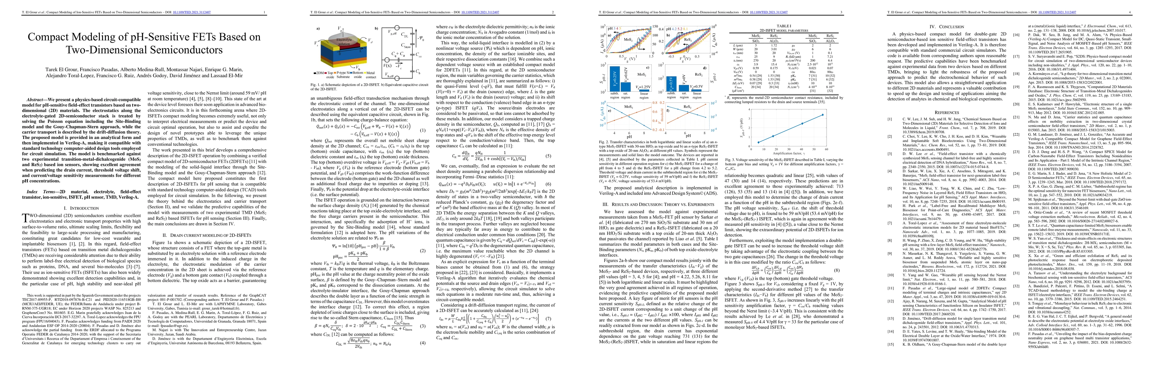
We present a physics-based circuit-compatible model for pH-sensitive field-effect transistors based on two-dimensional (2D) materials. The electrostatics along the electrolyte-gated 2D-semiconductor...

Thumbnail for Unveiling the impact of the bias-dependent charge neutrality point on
  graphene-based multi-transistor applications

Unveiling the impact of the bias-dependent charge neutrality point on graphene-based multi-transistor applications

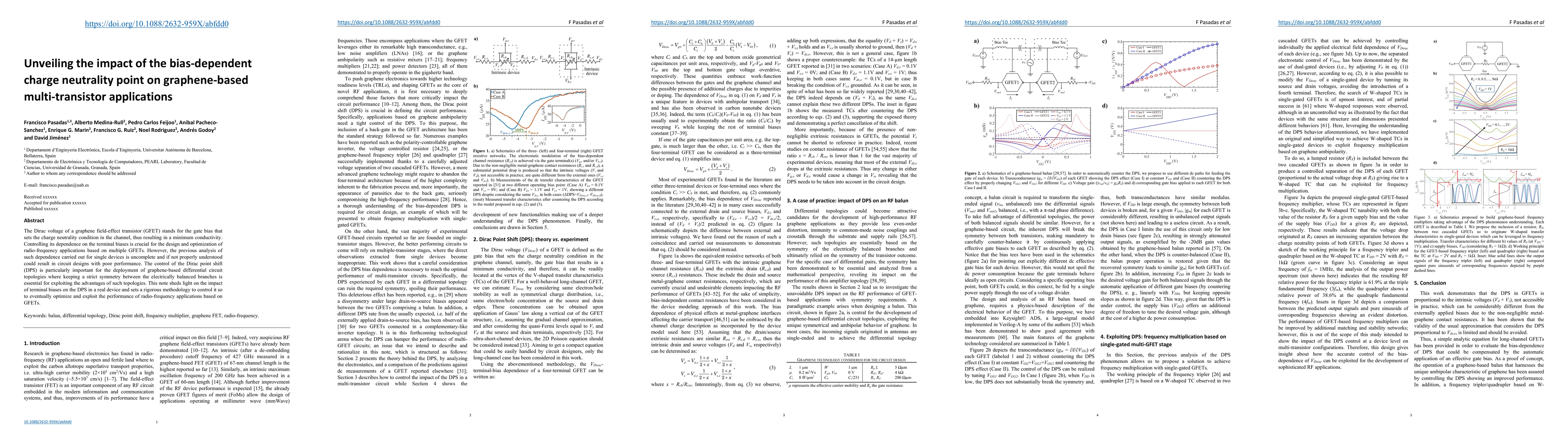
The Dirac voltage of a graphene field-effect transistor (GFET) stands for the gate bias that sets the charge neutrality condition in the channel, thus resulting in a minimum conductivity. Controllin...

Thumbnail for Large-signal model of 2DFETs: compact modeling of terminal charges and
  intrinsic capacitances

Large-signal model of 2DFETs: compact modeling of terminal charges and intrinsic capacitances

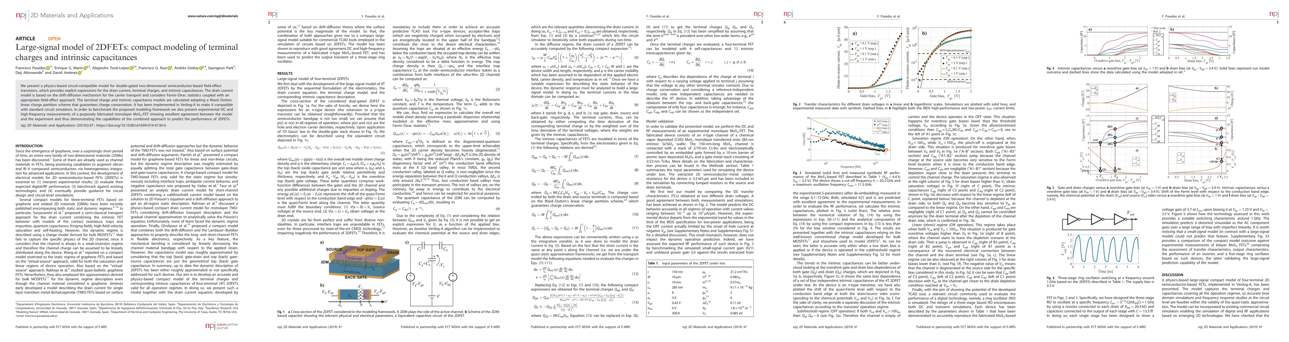
We present a physics-based circuit-compatible model for double-gated two-dimensional semiconductor based field effect transistors, which provides explicit expressions for the drain current, terminal...

Thumbnail for Lateral Heterostructure Field-Effect Transistors Based on 2D-Material
  Stacks With Varying Thickness and Energy Filtering Source

Lateral Heterostructure Field-Effect Transistors Based on 2D-Material Stacks With Varying Thickness and Energy Filtering Source

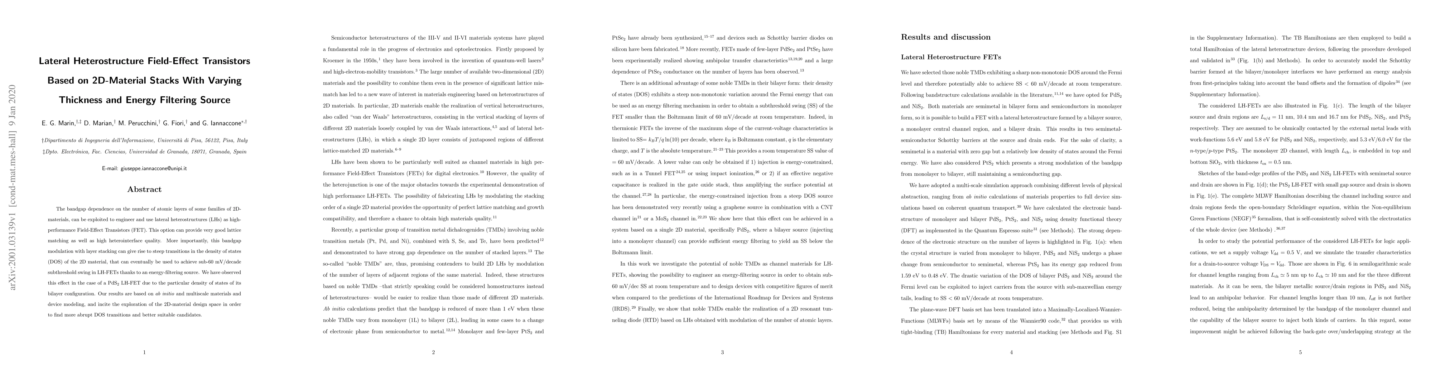
The bandgap dependence on the number of atomic layers of some families of 2D-materials, can be exploited to engineer and use lateral heterostructures (LHs) as high-performance Field-Effect Transisto...

Thumbnail for Understanding Memristive Behavior: An Atomistic Study of the Influence
  of Grain Boundaries on Surface and Out-of-Plane Diffusion of Metallic Atoms

Understanding Memristive Behavior: An Atomistic Study of the Influence of Grain Boundaries on Surface and Out-of-Plane Diffusion of Metallic Atoms

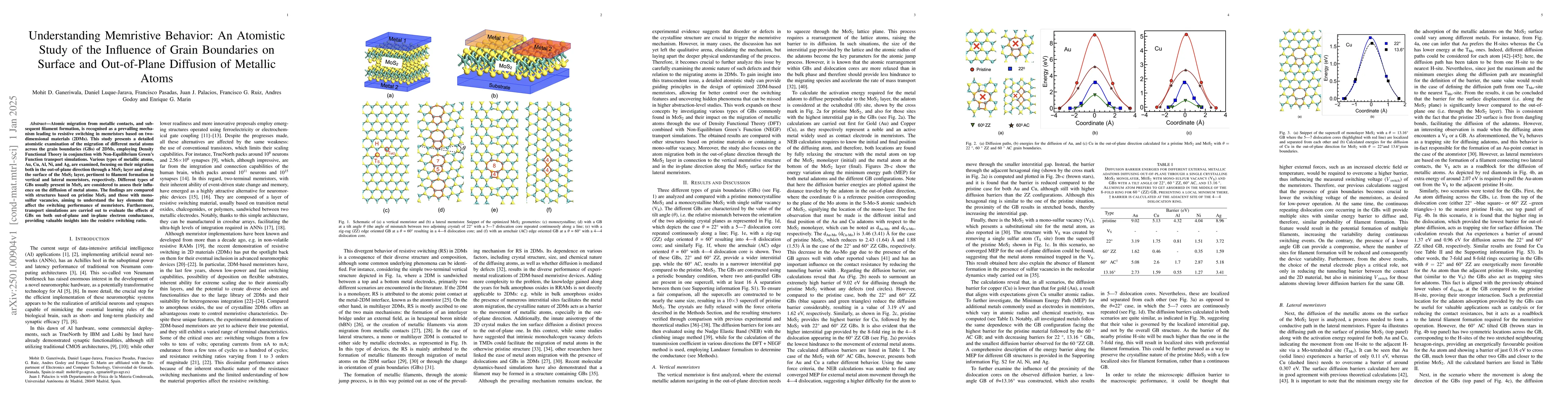
Atomic migration from metallic contacts, and subsequent filament formation, is recognised as a prevailing mechanism leading to resistive switching in memristors based on two-dimensional materials (2DM...

Thumbnail for Numerical study of synaptic behavior in amorphous HfO2-based
  ferroelectric-like FETs generated by voltage-driven ion migration

Numerical study of synaptic behavior in amorphous HfO2-based ferroelectric-like FETs generated by voltage-driven ion migration

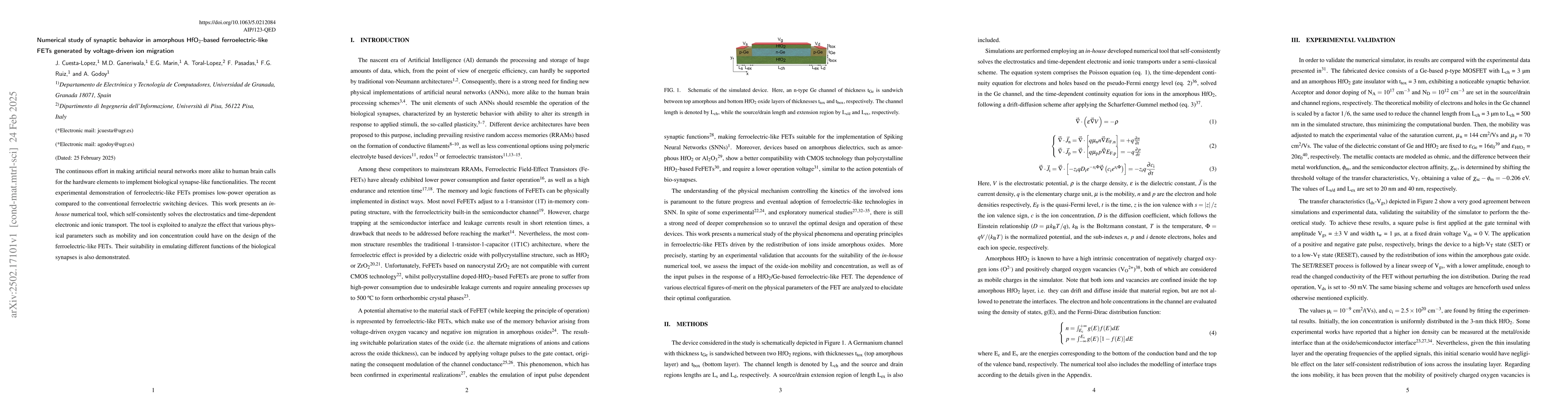
The continuous effort in making artificial neural networks more alike to human brain calls for the hardware elements to implement biological synapse-like functionalities. The recent experimental demon...

This website uses cookies to ensure you get the best experience. Learn more