Academic Profile
Statistics
Similar Authors
Papers on arXiv
Two-photon absorption in indirect gap semiconductors is an frequently encountered, but not well-understood phenomenon. To address this, the Real Density Matrix Approach is applied to describe two-ph...
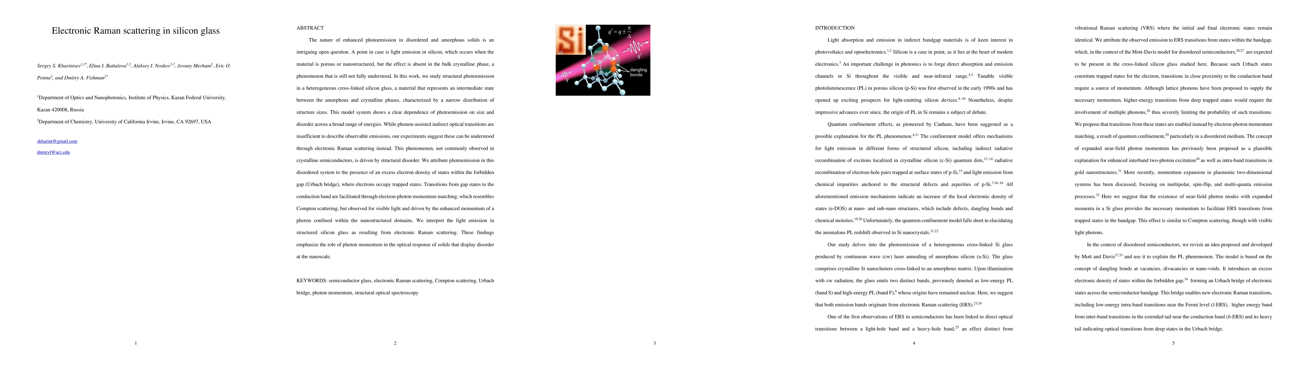
The nature of enhanced photoemission in disordered and amorphous solids is an intriguing open question. A point in case is light emission in silicon, which occurs when the material is porous or nano...
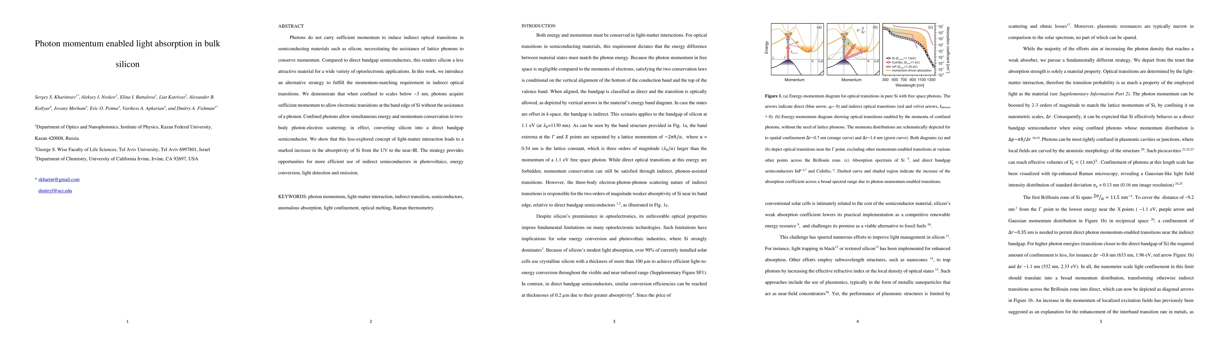
Photons do not carry sufficient momentum to induce indirect optical transitions in semiconducting materials such as silicon, necessitating the assistance of lattice phonons to conserve momentum. Com...
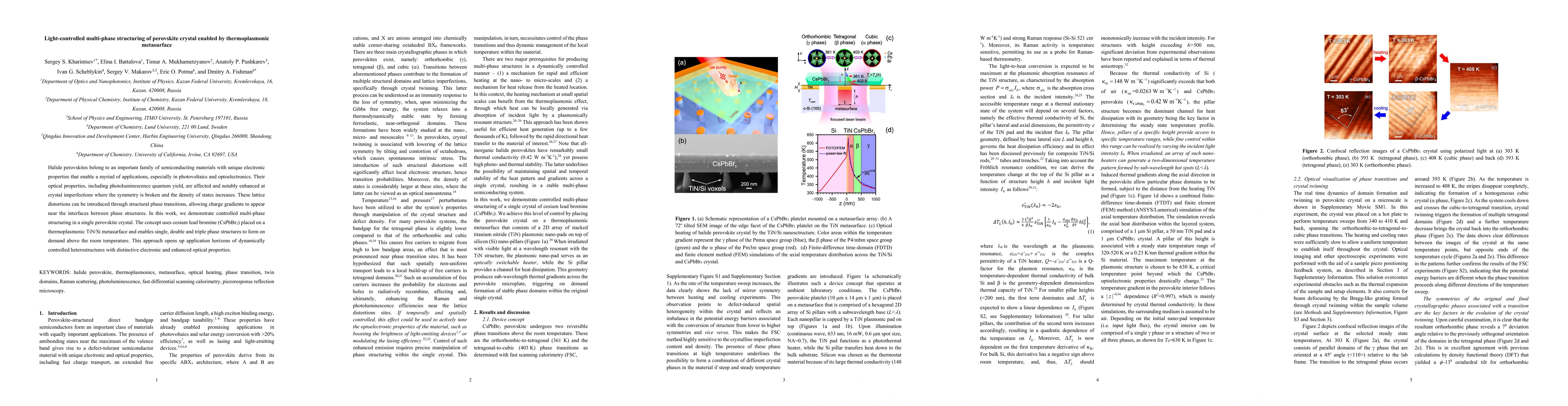
Halide perovskites belong to an important family of semiconducting materials with unique electronic properties that enable a myriad of applications, especially in photovoltaics and optoelectronics. ...
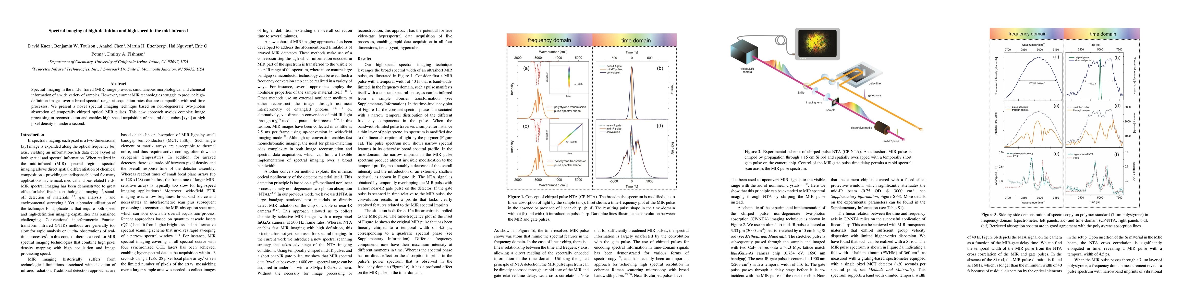
Spectral imaging in the mid-infrared (MIR) range provides simultaneous morphological and chemical information of a wide variety of samples. However, current MIR technologies struggle to produce high...
Many nanophotonic applications require precise control and characterization of electromagnetic field properties at the nanoscale. The chiral properties of the field are among its key characteristics...
Modern optical nano-elements pursue ever-smaller sizes and individualized functionalities. Those elements that can efficiently manipulate the magnetic field of light boast promising future applicati...
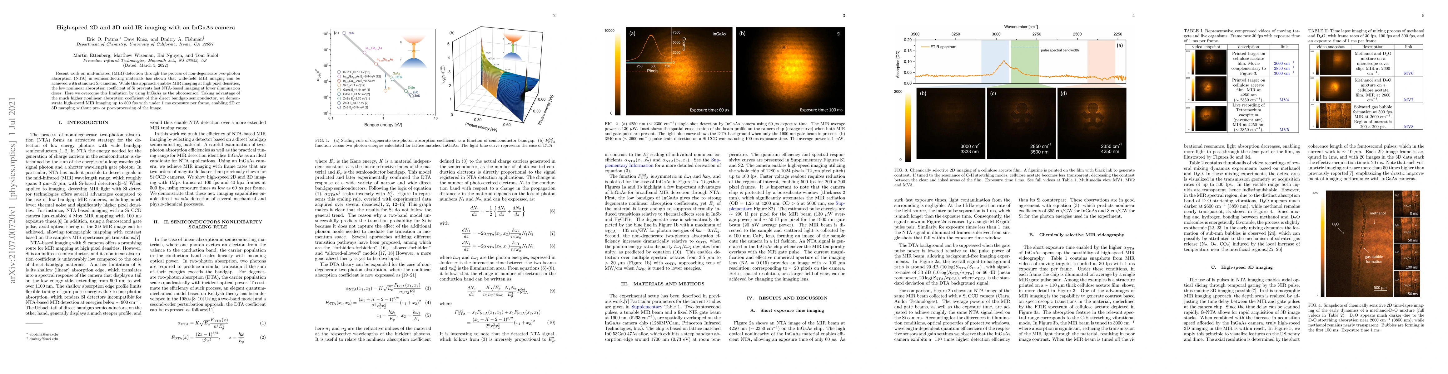
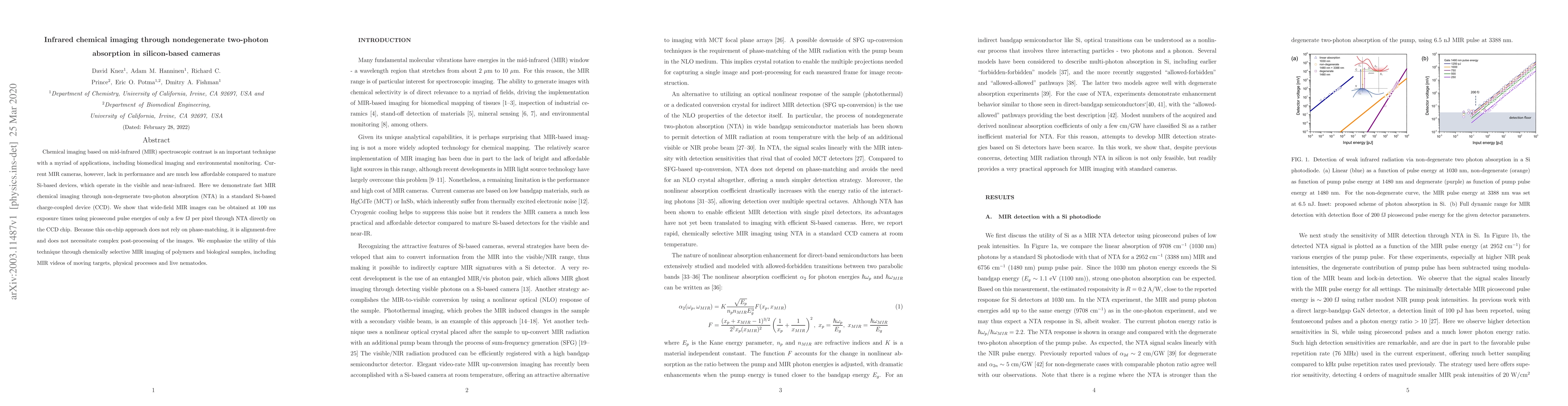
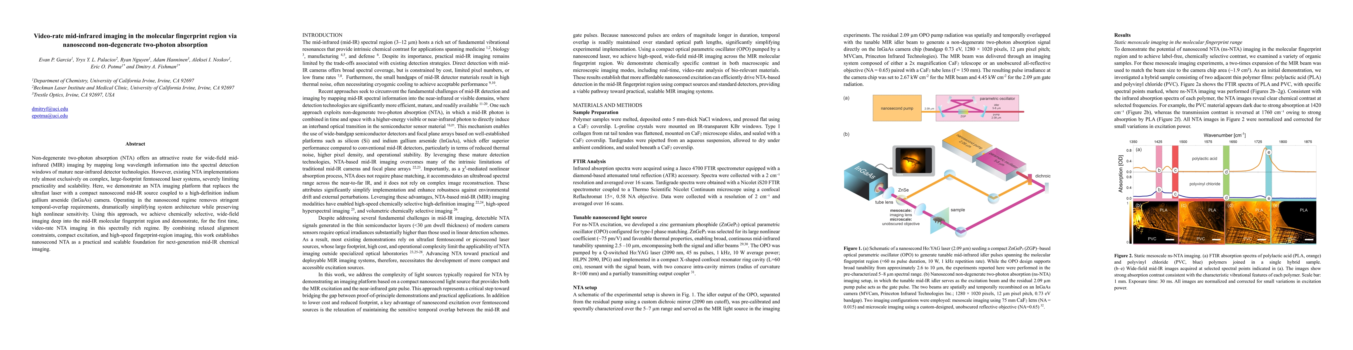
Recent work on mid-infrared (MIR) detection through the process of non-degenerate two-photon absorption (NTA) in semiconducting materials has shown that wide-field MIR imaging can be achieved with s...
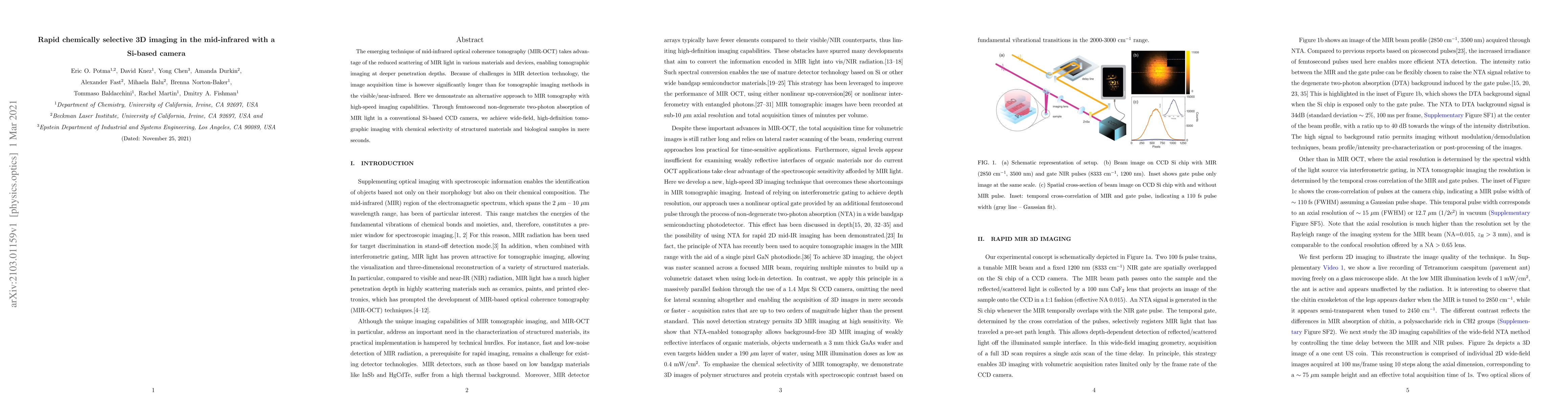
The emerging technique of mid-infrared optical coherence tomography (MIR-OCT) takes advantage of the reduced scattering of MIR light in various materials and devices, enabling tomographic imaging at...
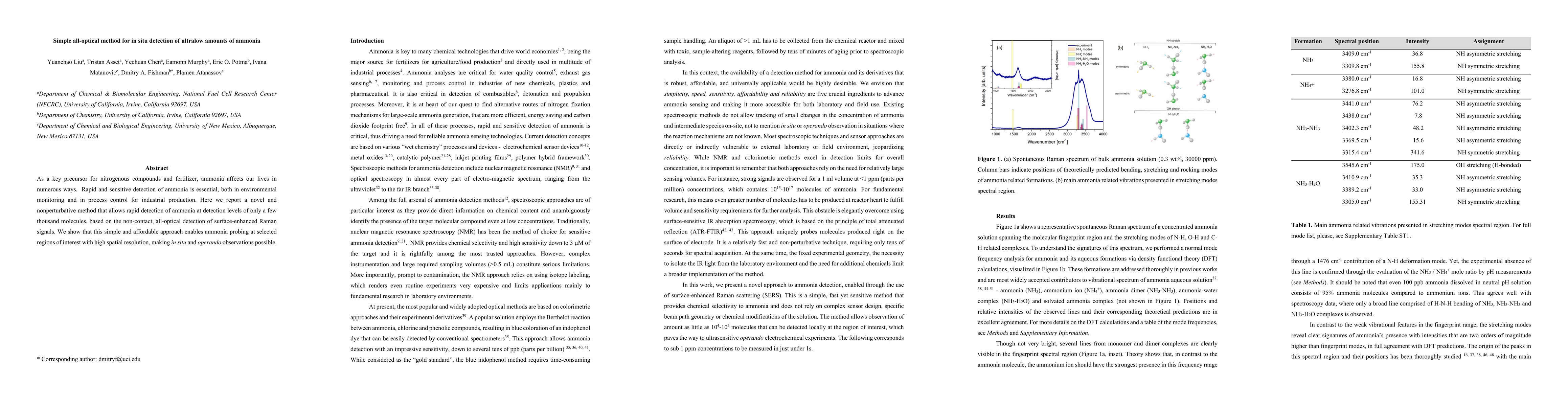
As a key precursor for nitrogenous compounds and fertilizer, ammonia affects our lives in numerous ways. Rapid and sensitive detection of ammonia is essential, both in environmental monitoring and i...
Chemical imaging based on mid-infrared (MIR) spectroscopic contrast is an important technique with a myriad of applications, including biomedical imaging and environmental monitoring. Current MIR ca...
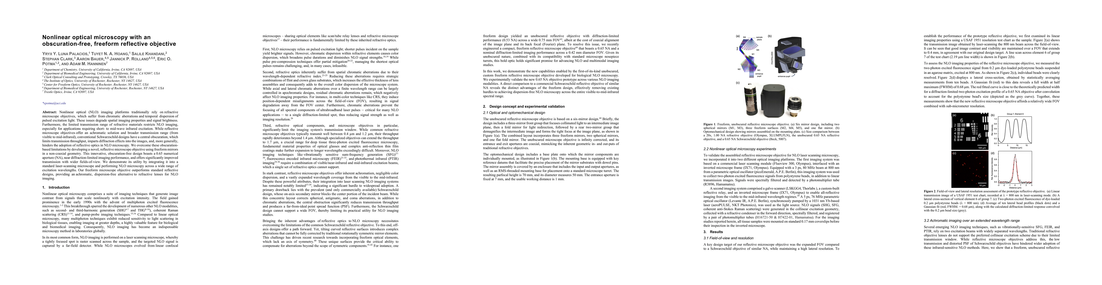
Nonlinear optical (NLO) imaging platforms traditionally rely on refractive microscope objectives, which suffer from chromatic aberrations and temporal dispersion of pulsed excitation light. These issu...
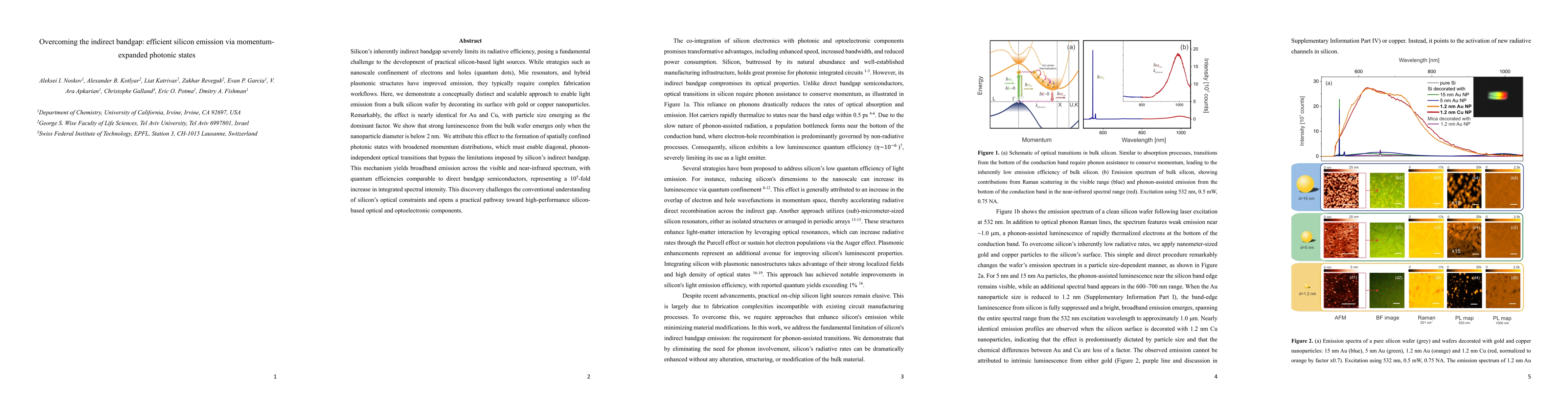
Silicon's inherently indirect bandgap severely limits its radiative efficiency, posing a fundamental challenge to the development of practical silicon-based light sources. While strategies such as nan...
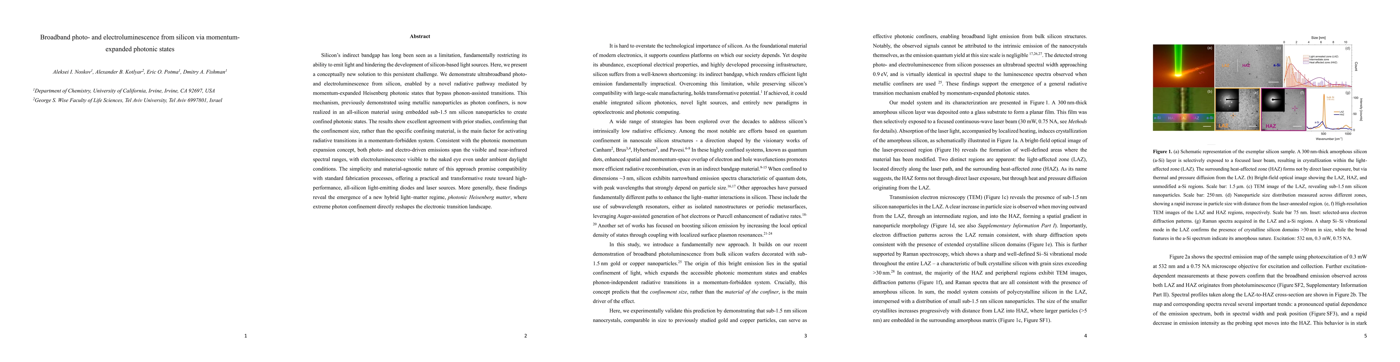
Silicon's indirect bandgap has long been seen as a limitation, fundamentally restricting its ability to emit light and hindering the development of silicon-based light sources. Here, we present a conc...
Non-degenerate two-photon absorption (NTA) offers an attractive route for wide-field mid-infrared (MIR) imaging by mapping long wavelength information into the spectral detection windows of mature nea...
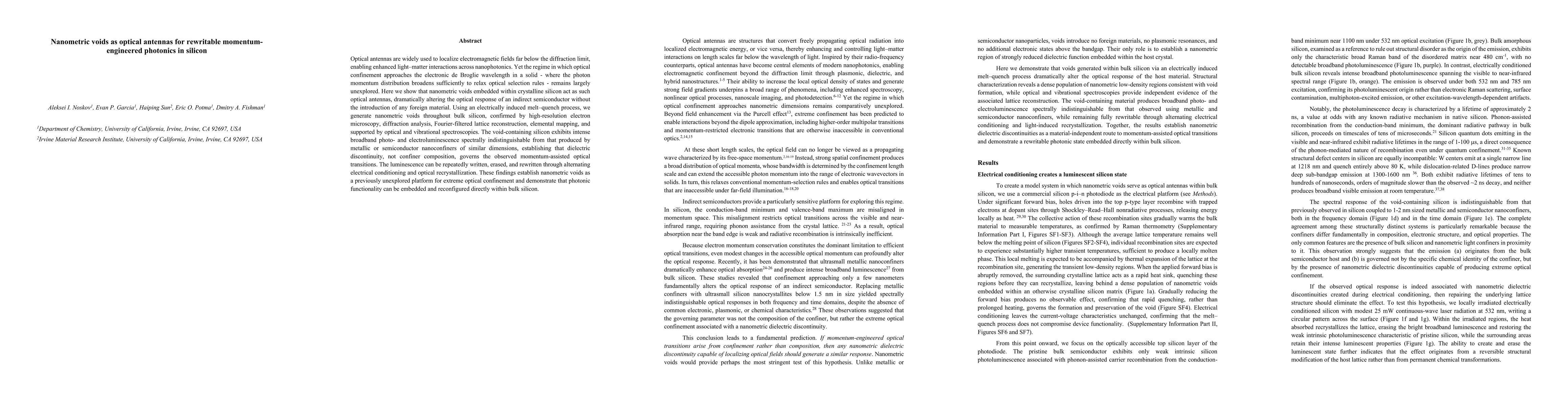
Optical antennas are widely used to localize electromagnetic fields far below the diffraction limit, enabling enhanced light-matter interactions across nanophotonics. Yet the regime in which optical c...