Academic Profile
Statistics
Similar Authors
Papers on arXiv
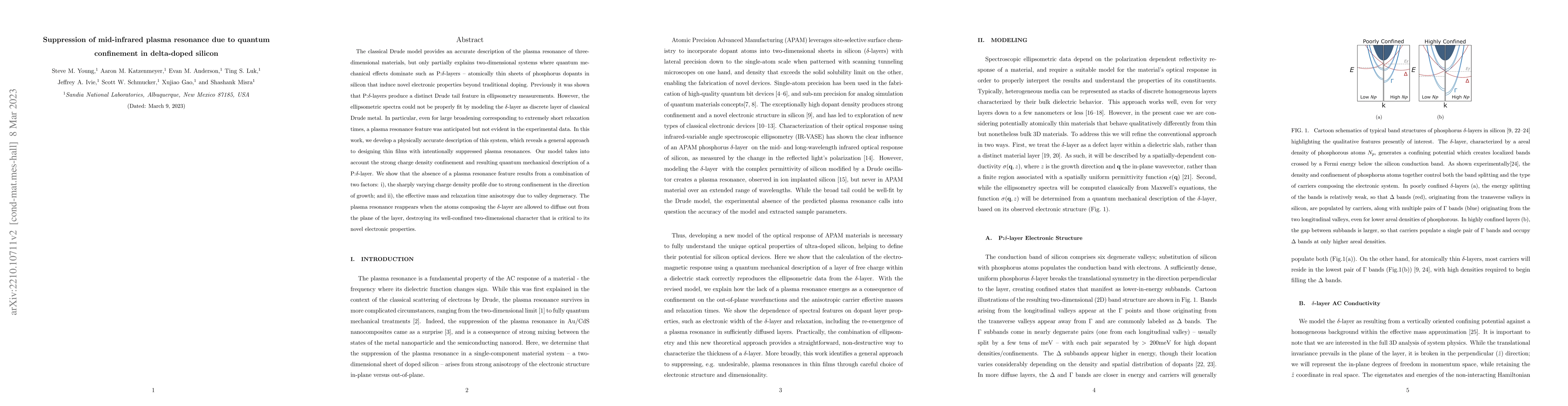
The classical Drude model provides an accurate description of the plasma resonance of three-dimensional materials, but only partially explains two-dimensional systems where quantum mechanical effect...
As transistor features shrink beyond the 2 nm node, studying and designing for atomic scale effects become essential. Being able to combine conventional CMOS with new atomic scale fabrication routes...
An exponential increase in the performance of silicon microelectronics and the demand to manufacture in great volumes has created an ecosystem that requires increasingly complex tools to fabricate a...
Spin states in semiconductors provide exceptionally stable and noise-resistant environments for qubits, positioning them as optimal candidates for reliable quantum computing technologies. The proposal...
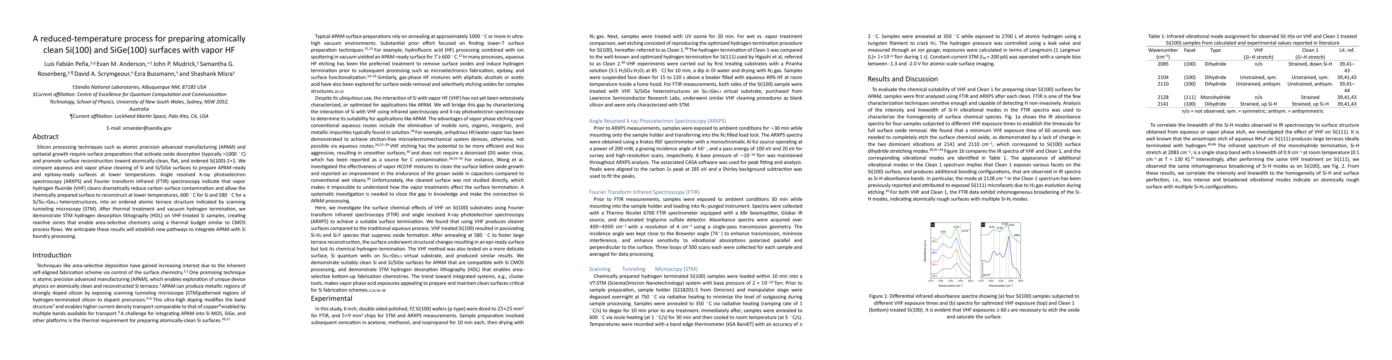
Silicon processing techniques such as atomic precision advanced manufacturing (APAM) and epitaxial growth require surface preparations that activate oxide desorption (typically >1000 $^{\circ}$C) and ...
Characterizing intrinsic defects is an important step in evaluating materials for new optoelectronic device applications. For photomultipliers, suppressing dark currents is critical, but there exists ...
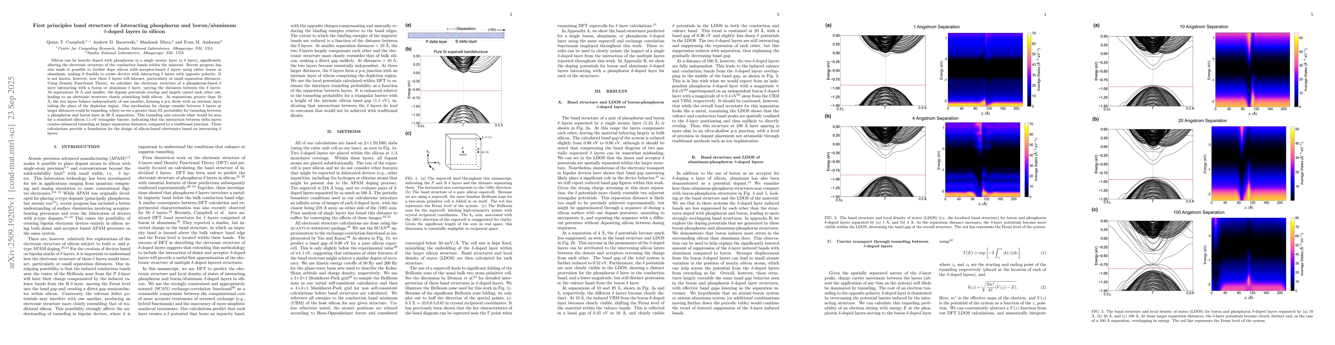
Silicon can be heavily doped with phosphorus in a single atomic layer (a $\delta$ layer), significantly altering the electronic structure of the conduction bands within the material. Recent progress h...
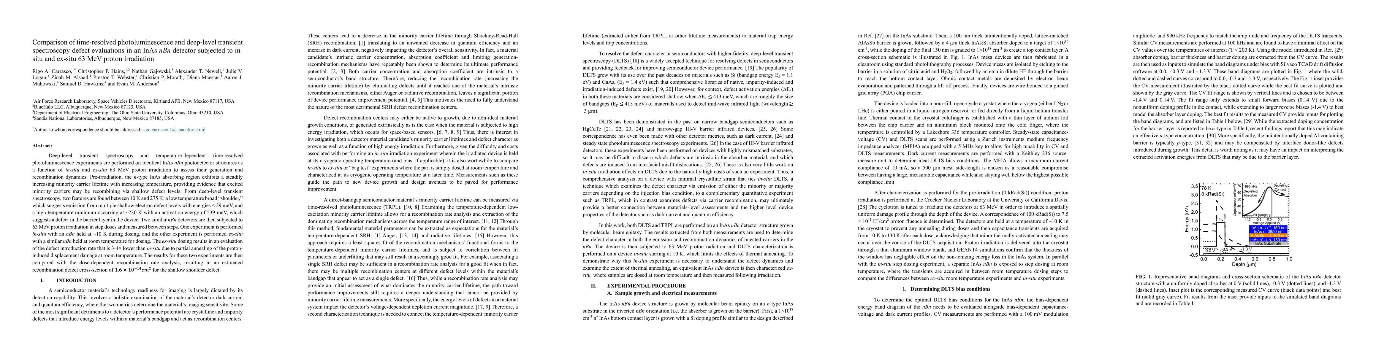
Deep-level transient spectroscopy and temperature-dependent time-resolved photoluminescence experiments are performed on identical InAs nBn photodetector structures as a function of in-situ and ex-sit...