Academic Profile
Statistics
Similar Authors
Papers on arXiv
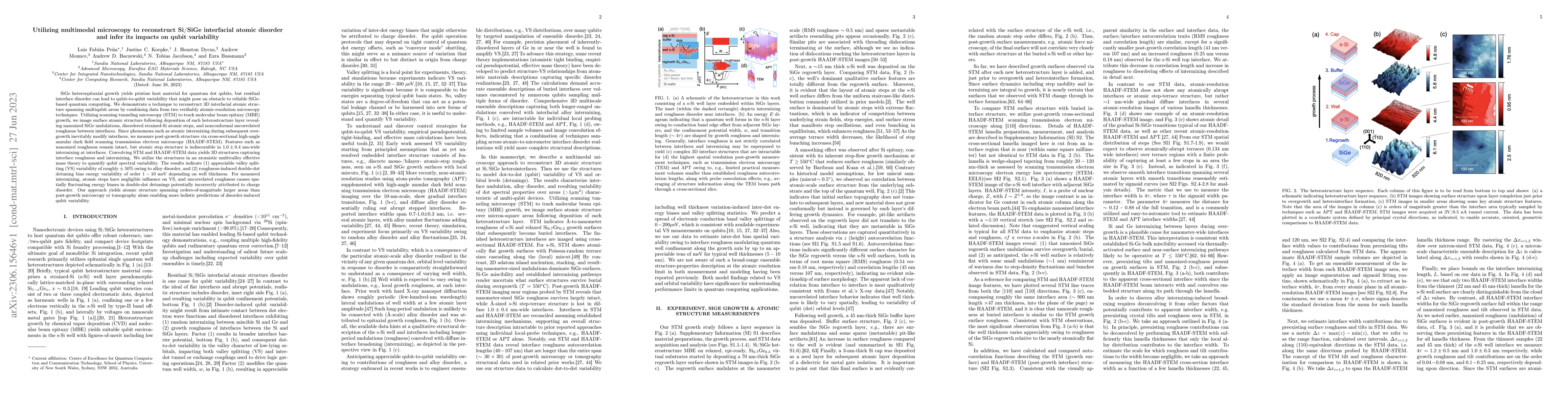
SiGe heteroepitaxial growth yields pristine host material for quantum dot qubits, but residual interface disorder can lead to qubit-to-qubit variability that might pose an obstacle to reliable SiGe-...
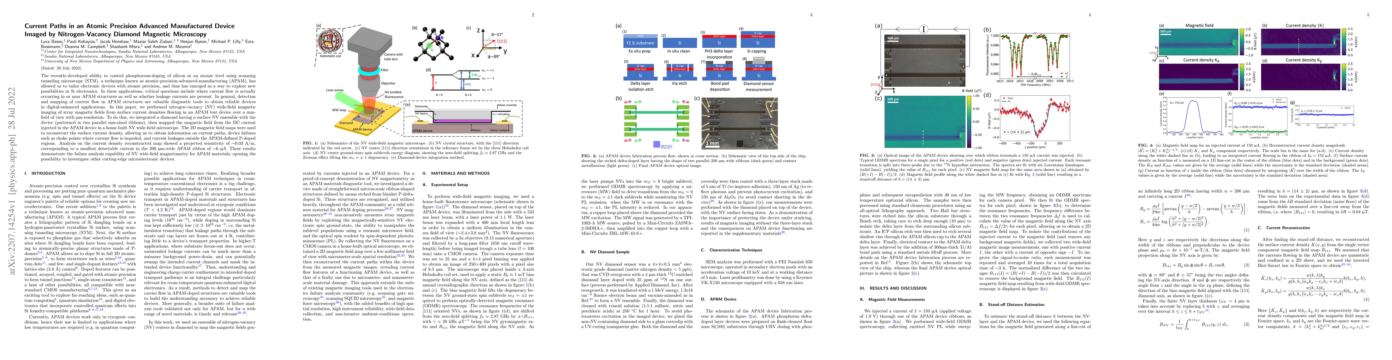
The recently-developed ability to control phosphorous-doping of silicon at an atomic level using scanning tunneling microscopy (STM), a technique known as atomic-precision-advanced-manufacturing (AP...
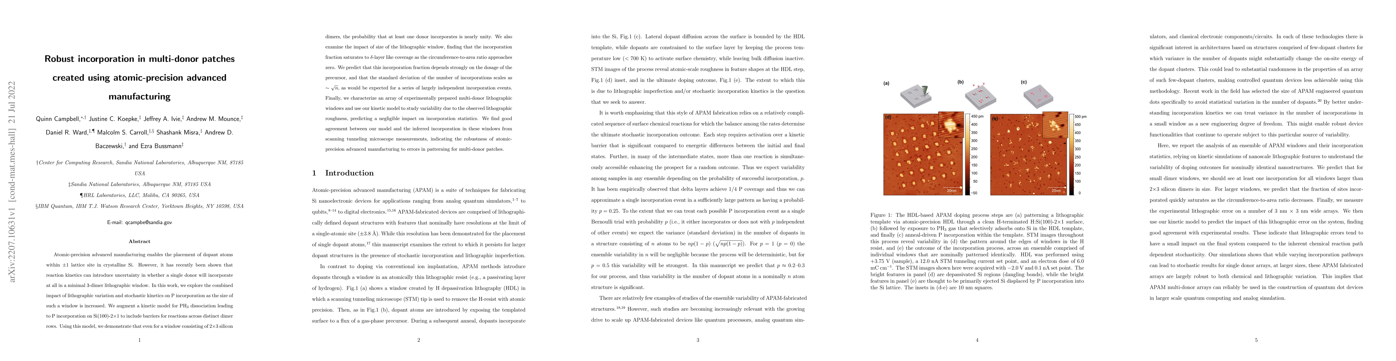
Atomic-precision advanced manufacturing enables the placement of dopant atoms within $\pm$1 lattice site in crystalline Si. However, it has recently been shown that reaction kinetics can introduce u...
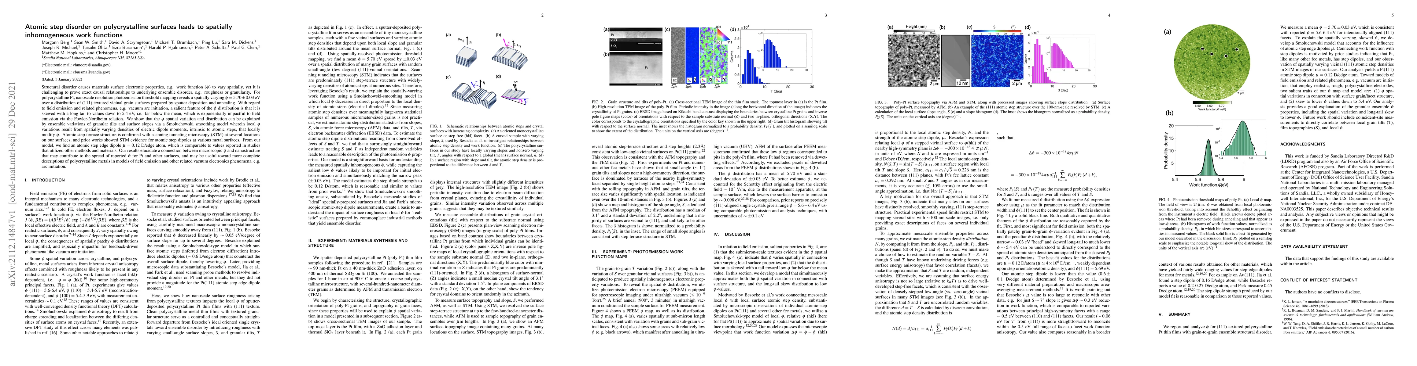
Structural disorder causes materials surface electronic properties, e.g. work function ($\phi$) to vary spatially, yet it is challenging to prove exact causal relationships to underlying ensemble di...
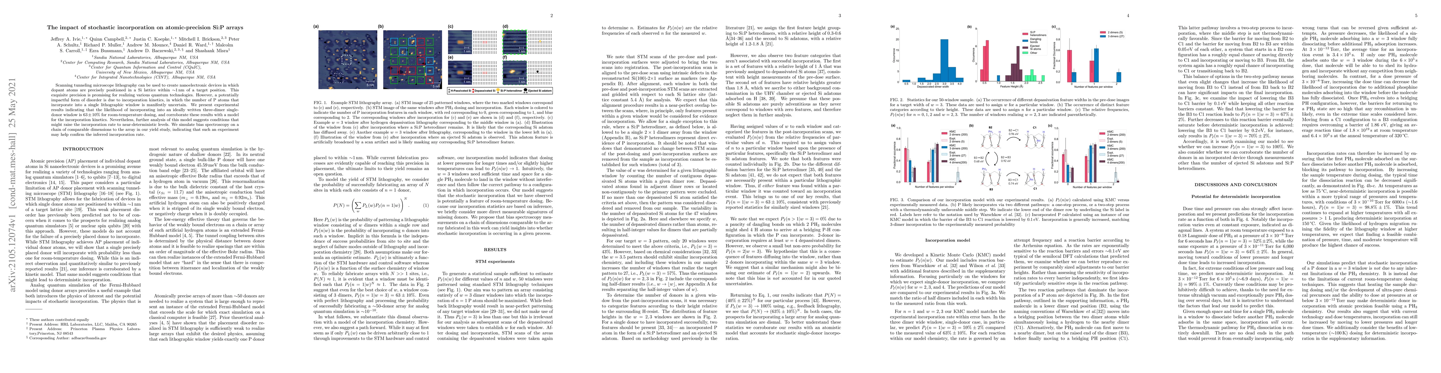
Scanning tunneling microscope lithography can be used to create nanoelectronic devices in which dopant atoms are precisely positioned in a Si lattice within $\sim$1 nm of a target position. This exq...
The adsorption of AlCl$_{3}$ on Si(100) and the effect of annealing the AlCl$_{3}$-dosed substrate was studied to reveal key surface processes for the development of atomic-precision acceptor-doping...
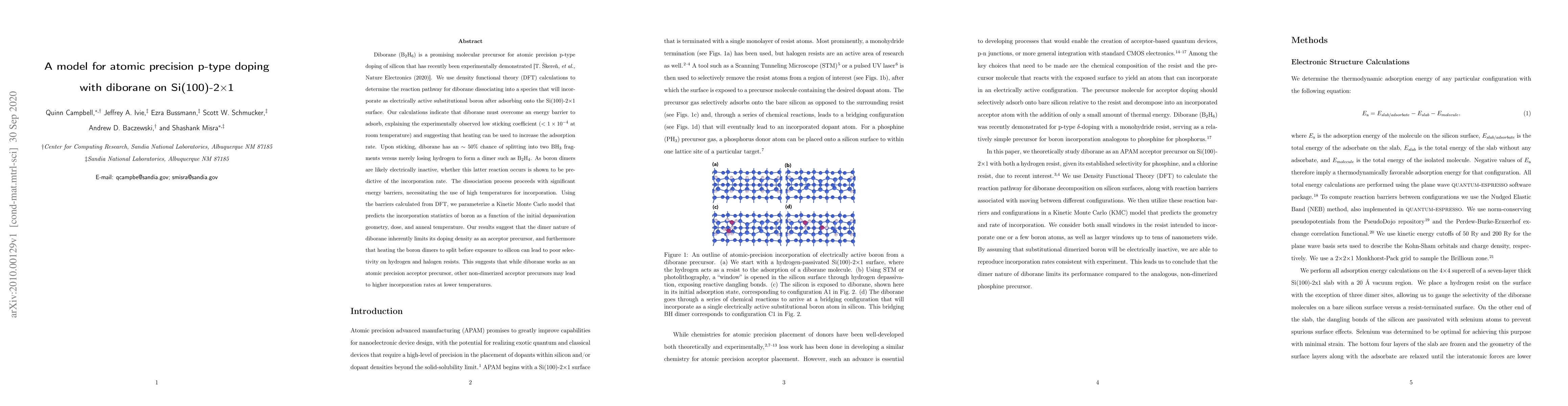
Diborane (B$_2$H$_6$) is a promising molecular precursor for atomic precision p-type doping of silicon that has recently been experimentally demonstrated [T. {\v{S}}kere{\v{n}}, \textit{et al.,} Nat...
An exponential increase in the performance of silicon microelectronics and the demand to manufacture in great volumes has created an ecosystem that requires increasingly complex tools to fabricate a...
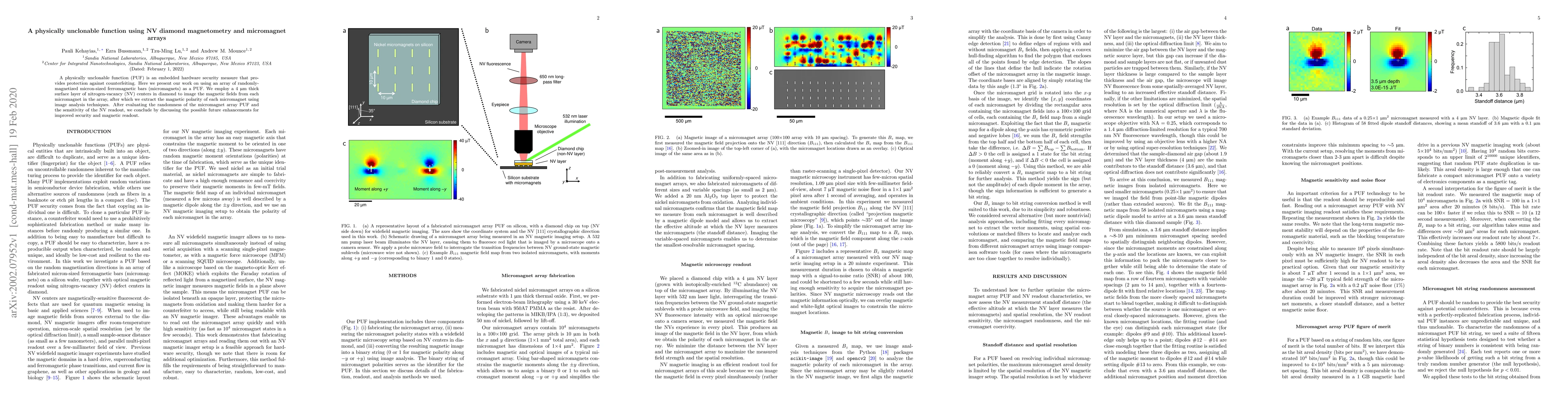
A physically unclonable function (PUF) is an embedded hardware security measure that provides protection against counterfeiting. Here we present our work on using an array of randomly-magnetized mic...
Spin states in semiconductors provide exceptionally stable and noise-resistant environments for qubits, positioning them as optimal candidates for reliable quantum computing technologies. The proposal...
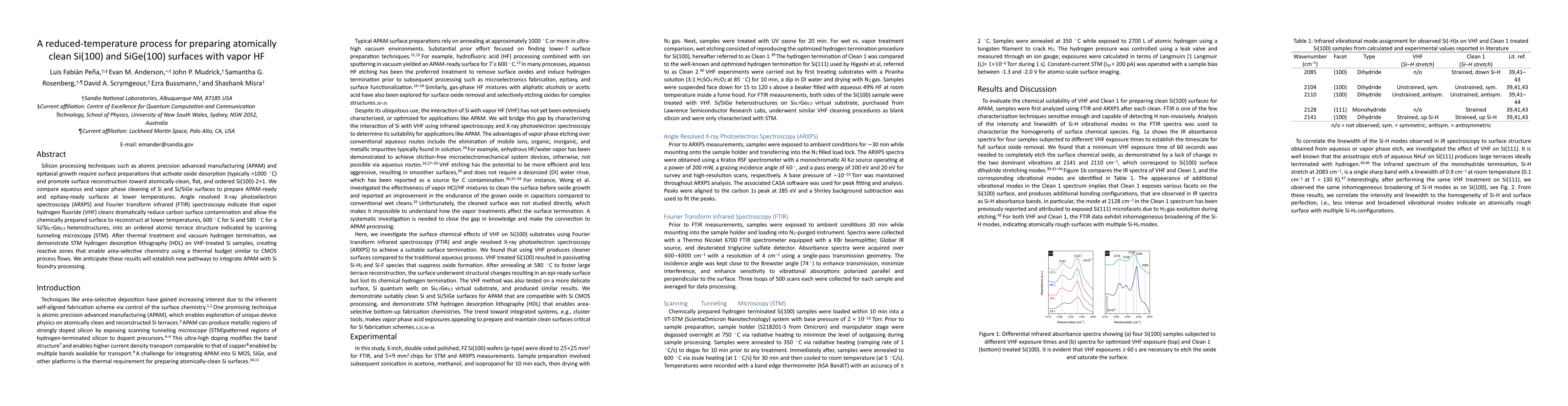
Silicon processing techniques such as atomic precision advanced manufacturing (APAM) and epitaxial growth require surface preparations that activate oxide desorption (typically >1000 $^{\circ}$C) and ...
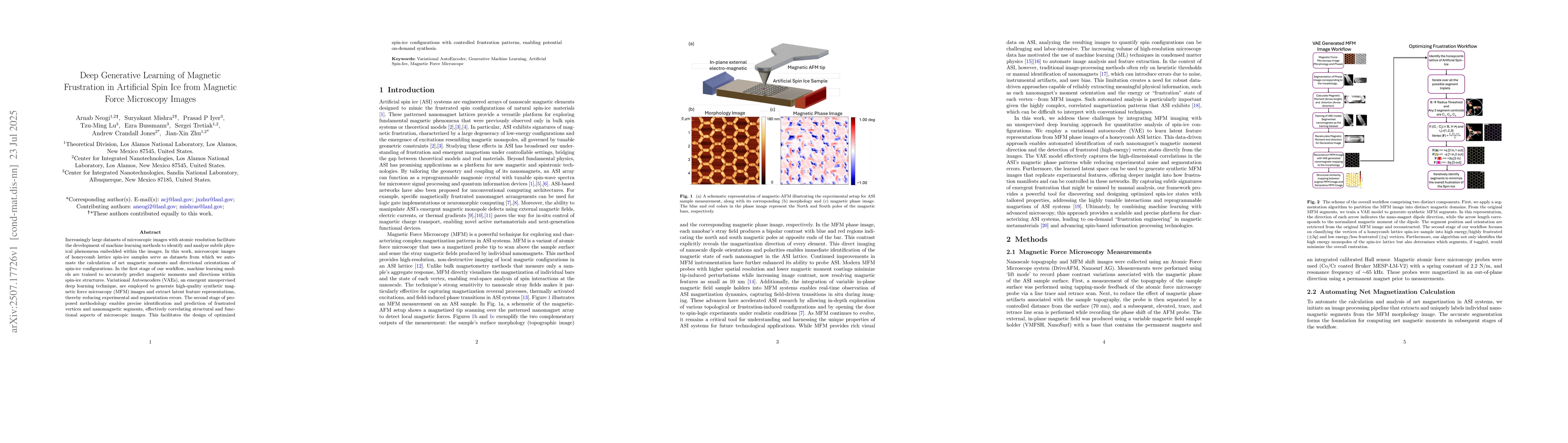
Increasingly large datasets of microscopic images with atomic resolution facilitate the development of machine learning methods to identify and analyze subtle physical phenomena embedded within the im...
SiGe heterostructures integrated with Si via virtual substrate (VS) growth are promising hosts for spin qubits. While VS growth targets plastic relaxation, residual cross-hatch strain inhomogeneity pr...