Academic Profile
Statistics
Similar Authors
Papers on arXiv
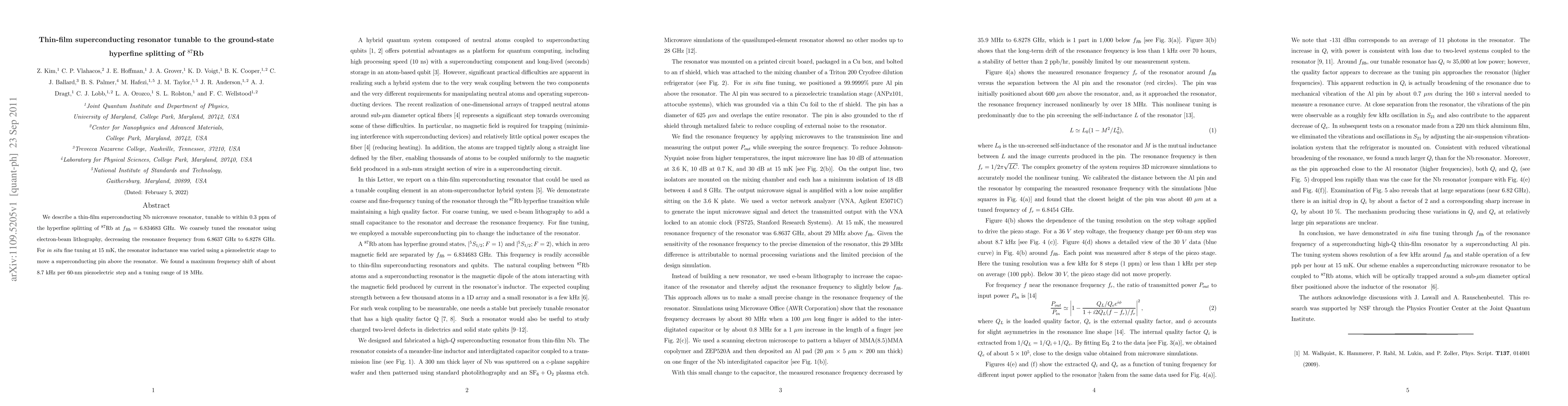
We describe a thin-film superconducting Nb microwave resonator, tunable to within 0.3 ppm of the hyperfine splitting of $^{87}$Rb at $f_{Rb}=6.834683$ GHz. We coarsely tuned the resonator using elec...
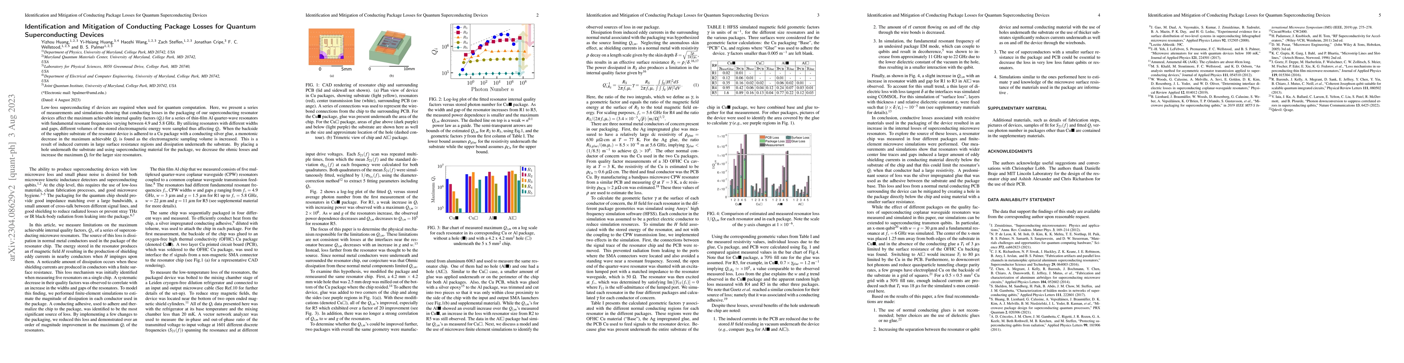
Low-loss superconducting rf devices are required when used for quantum computation. Here, we present a series of measurements and simulations showing that conducting losses in the packaging of our s...
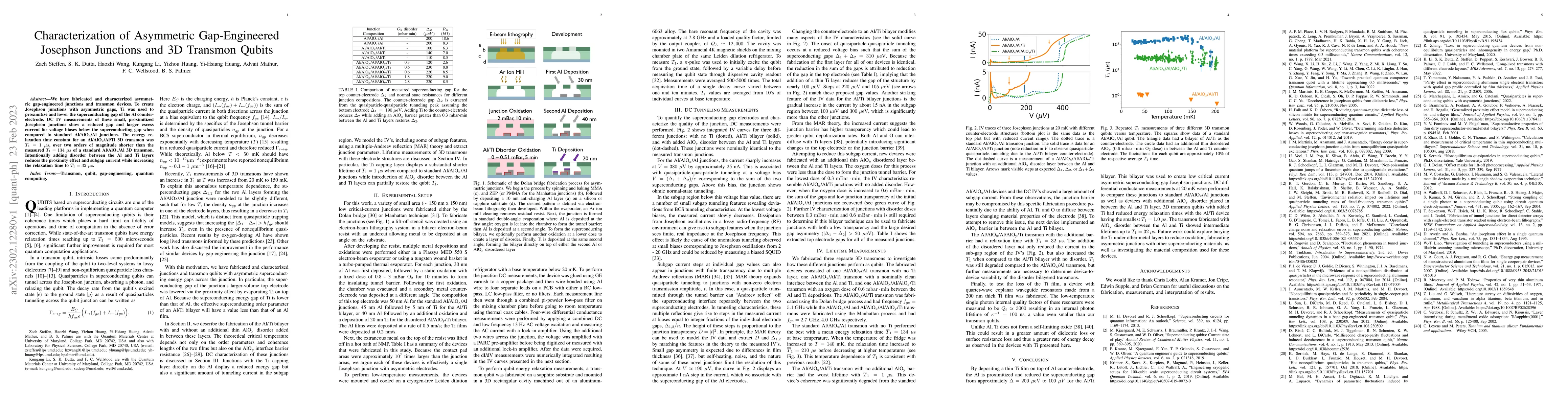
We have fabricated and characterized asymmetric gap-engineered junctions and transmon devices. To create Josephson junctions with asymmetric gaps, Ti was used to proximitize and lower the supercondu...
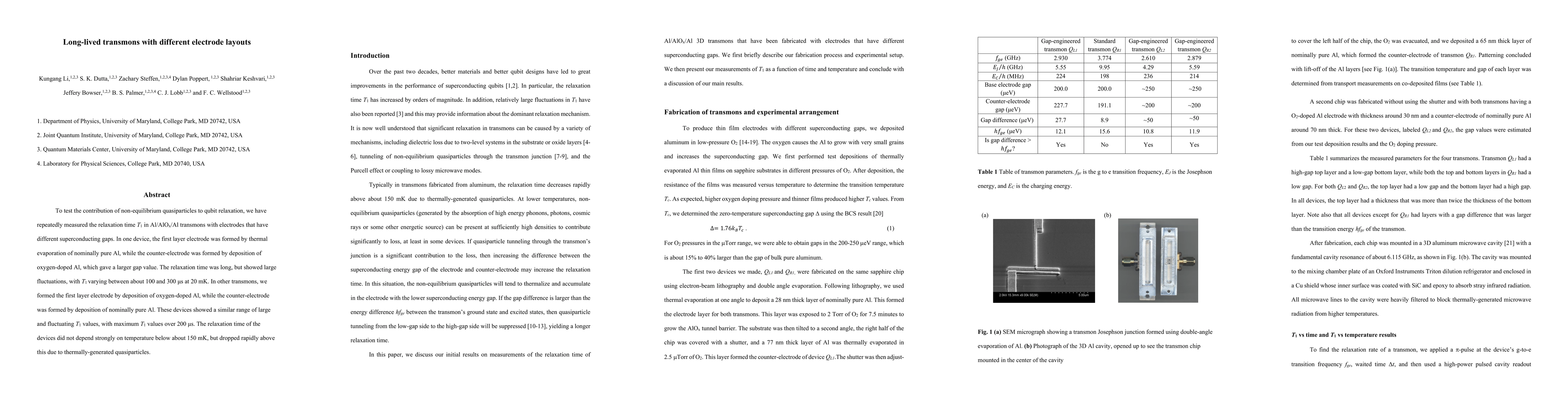
To test the contribution of non-equilibrium quasiparticles to qubit relaxation, we have repeatedly measured the relaxation time T_1 in Al/AlOx/Al transmons with electrodes that have different superc...
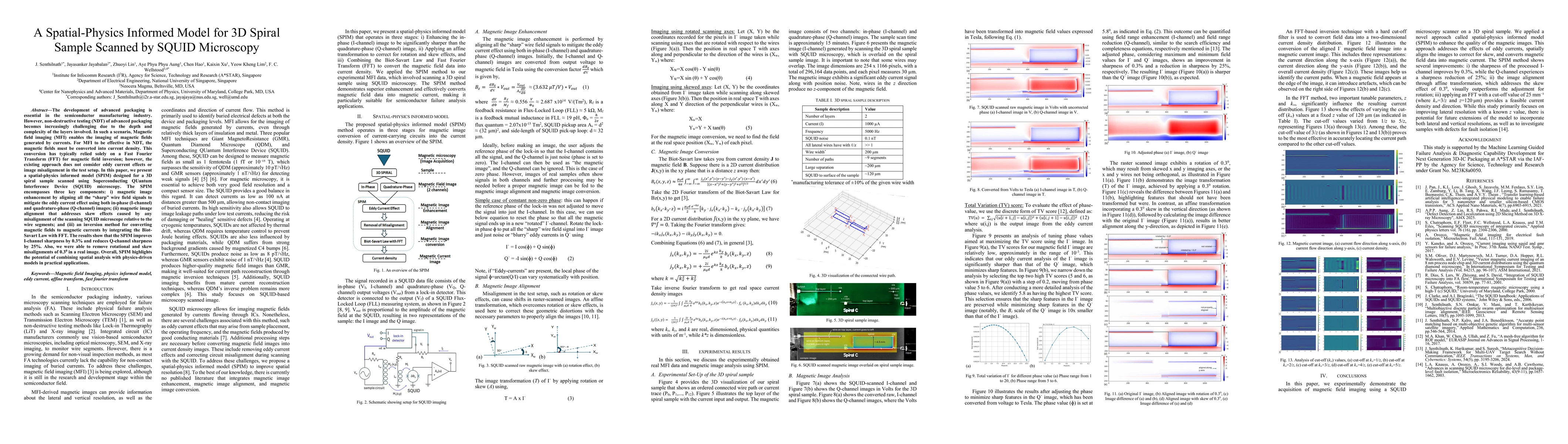
The development of advanced packaging is essential in the semiconductor manufacturing industry. However, non-destructive testing (NDT) of advanced packaging becomes increasingly challenging due to the...
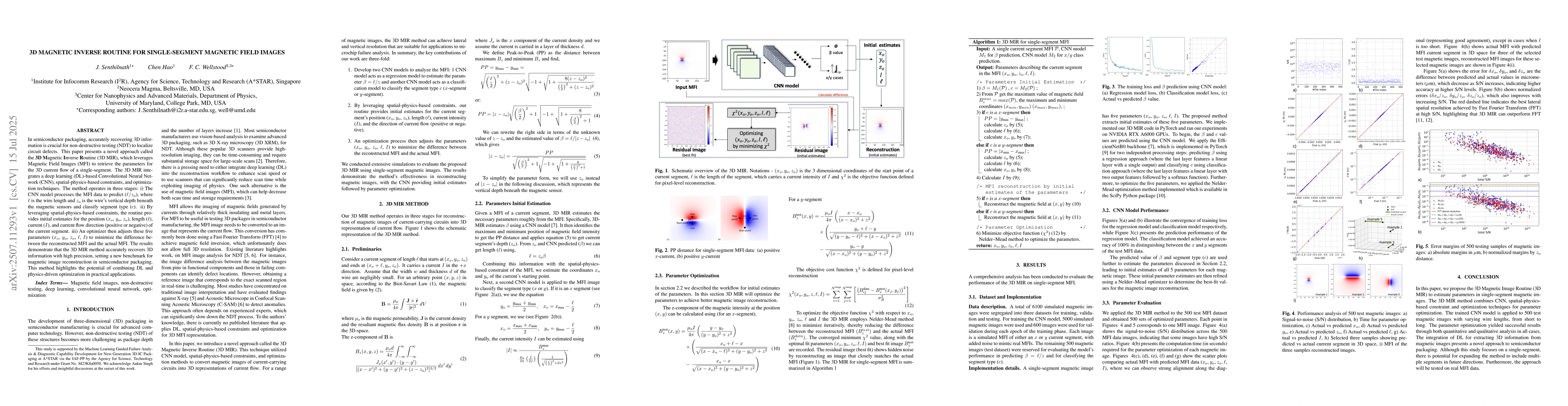
In semiconductor packaging, accurately recovering 3D information is crucial for non-destructive testing (NDT) to localize circuit defects. This paper presents a novel approach called the 3D Magnetic I...
We have examined the electrical behavior of Josephson junctions formed by a scanning tunneling microscope (STM) with a Nb sample and a Nb tip, with normal-state resistances Rn varying between 1 kOhm a...