Academic Profile
Statistics
Similar Authors
Papers on arXiv
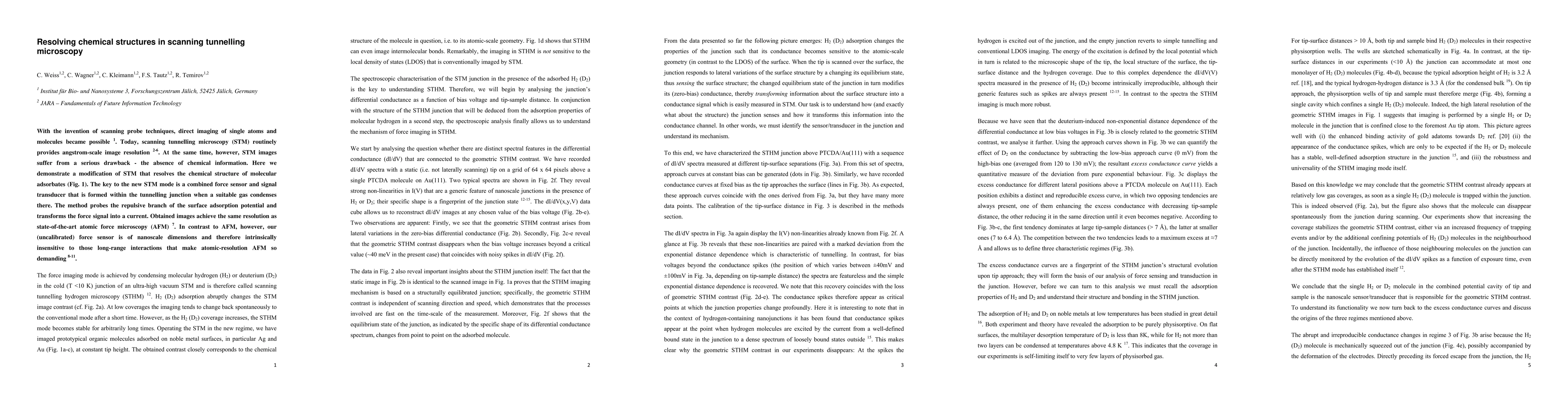
With the invention of scanning probe techniques, direct imaging of single atoms and molecules became possible. Today, scanning tunnelling microscopy (STM) routinely provides angstrom-scale image res...
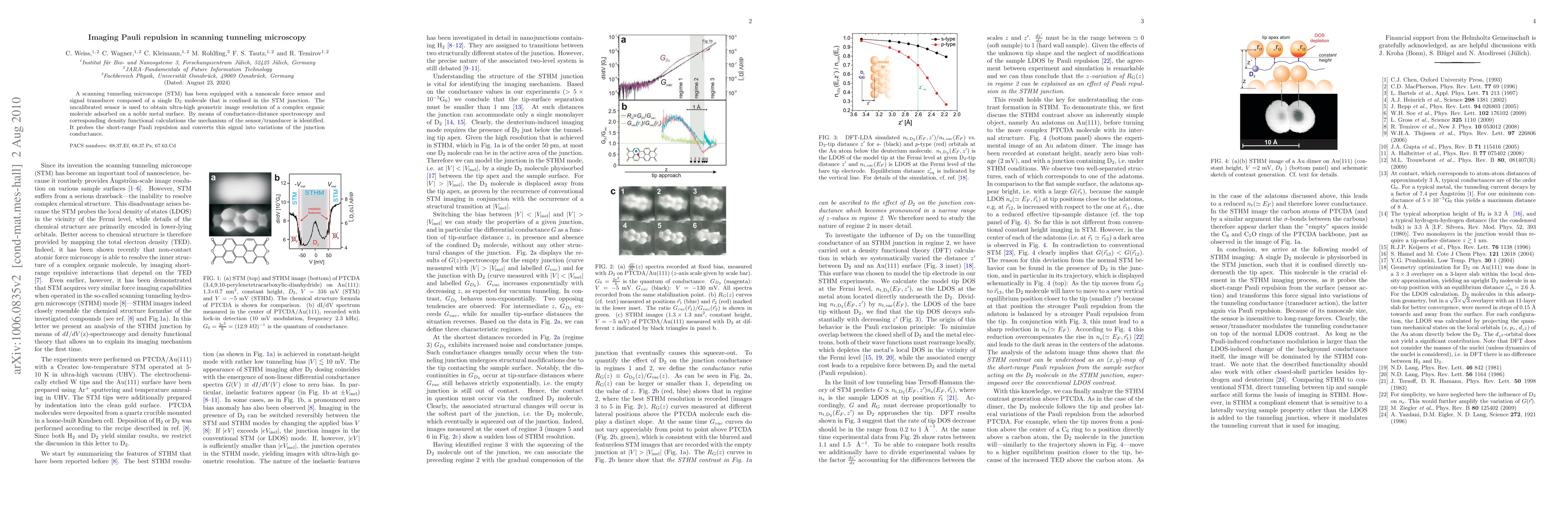
A scanning tunneling microscope (STM) has been equipped with a nanoscale force sensor and signal transducer composed of a single D2 molecule that is confined in the STM junction. The uncalibrated se...
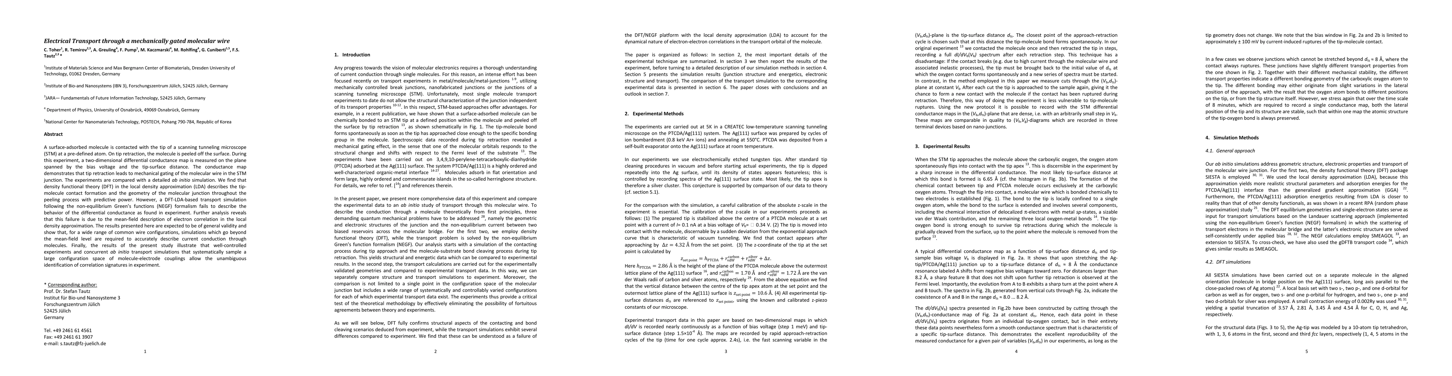
A surface-adsorbed molecule is contacted with the tip of a scanning tunneling microscope (STM) at a pre-defined atom. On tip retraction, the molecule is peeled off the surface. During this experimen...
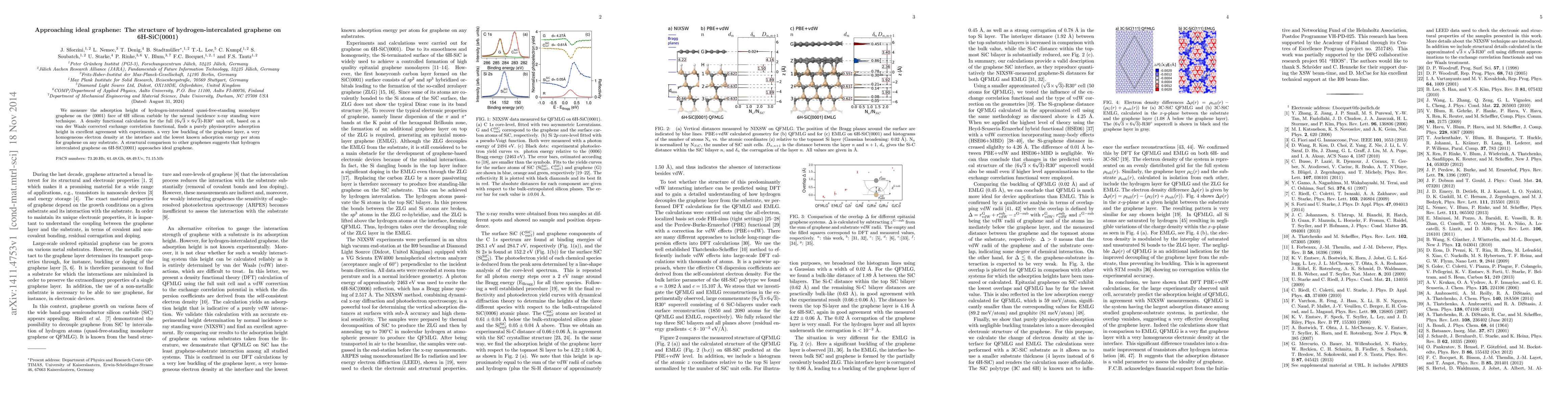
We measure the adsorption height of hydrogen-intercalated quasi-free-standing monolayer graphene on the (0001) face of 6H silicon carbide by the normal incidence x-ray standing wave technique. A den...
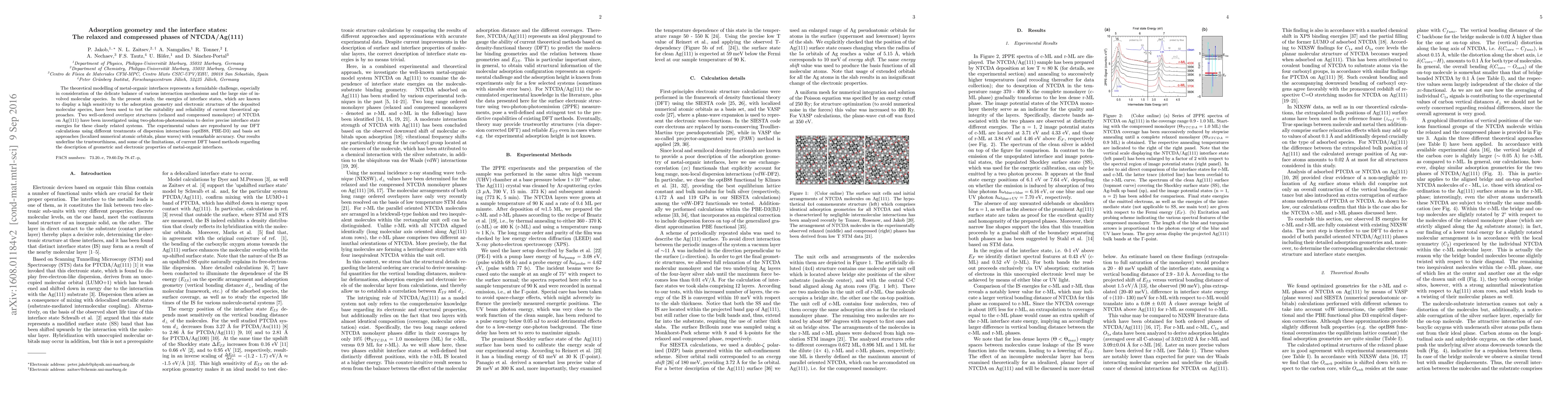
The theoretical modelling of metal-organic interfaces represents a formidable challenge, especially in consideration of the delicate balance of various interaction mechanisms and the large size of i...

Conductance measurements of a molecular wire, contacted between an epitaxial molecule-metal bond and the tip of a scanning tunneling microscope, are reported. Controlled retraction of the tip gradua...
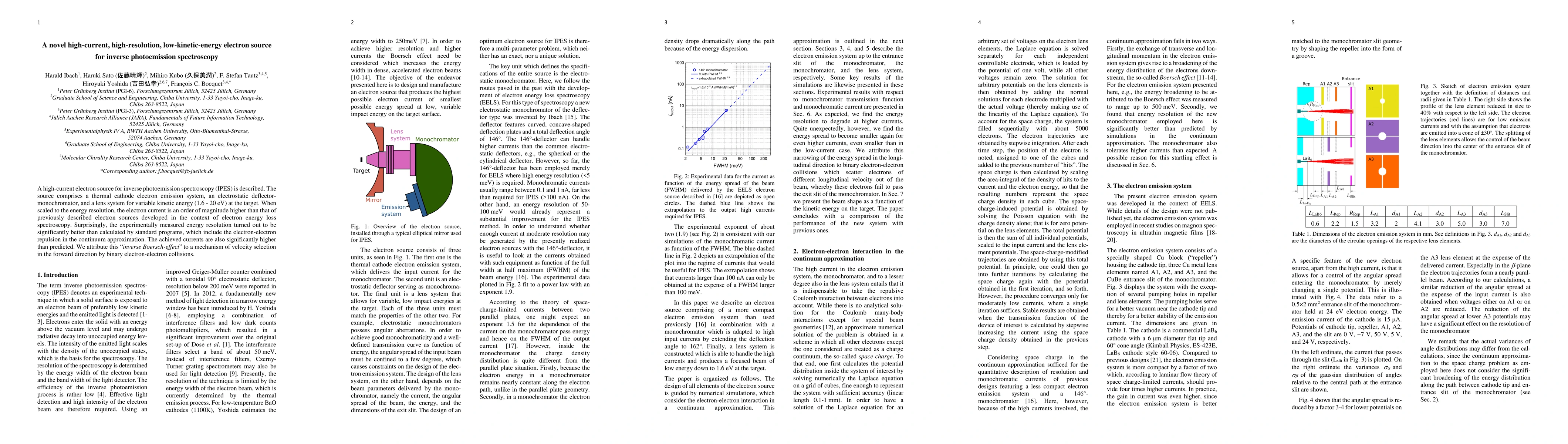
A high-current electron source for inverse photoemission spectroscopy (IPES) is described. The source comprises a thermal cathode electron emission system, an electrostatic deflector-monochromator, ...
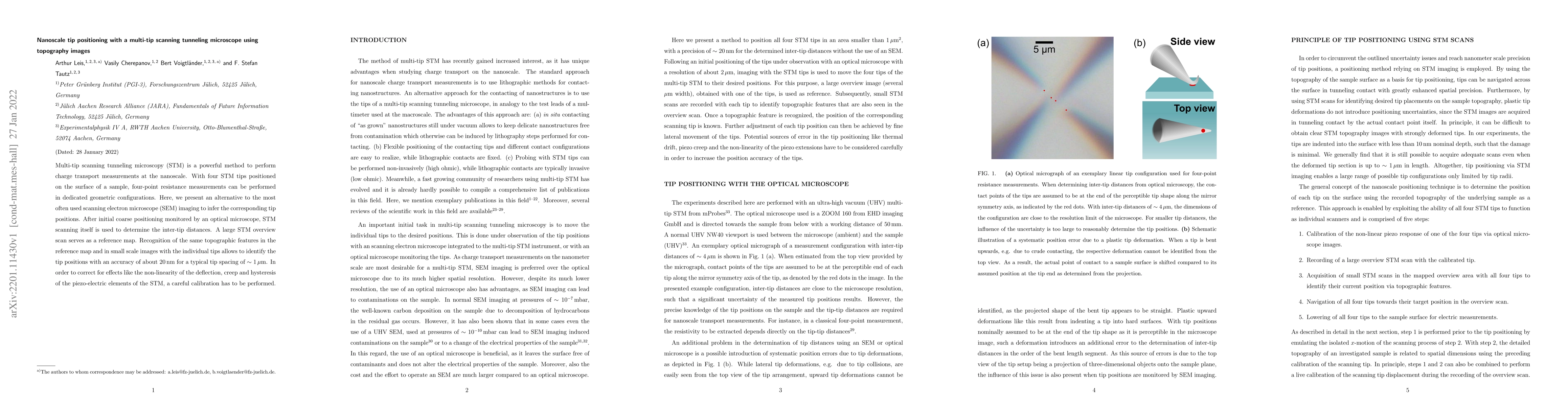
Multi-tip scanning tunneling microscopy (STM) is a powerful method to perform charge transport measurements at the nanoscale. With four STM tips positioned on the surface of a sample, four-point res...
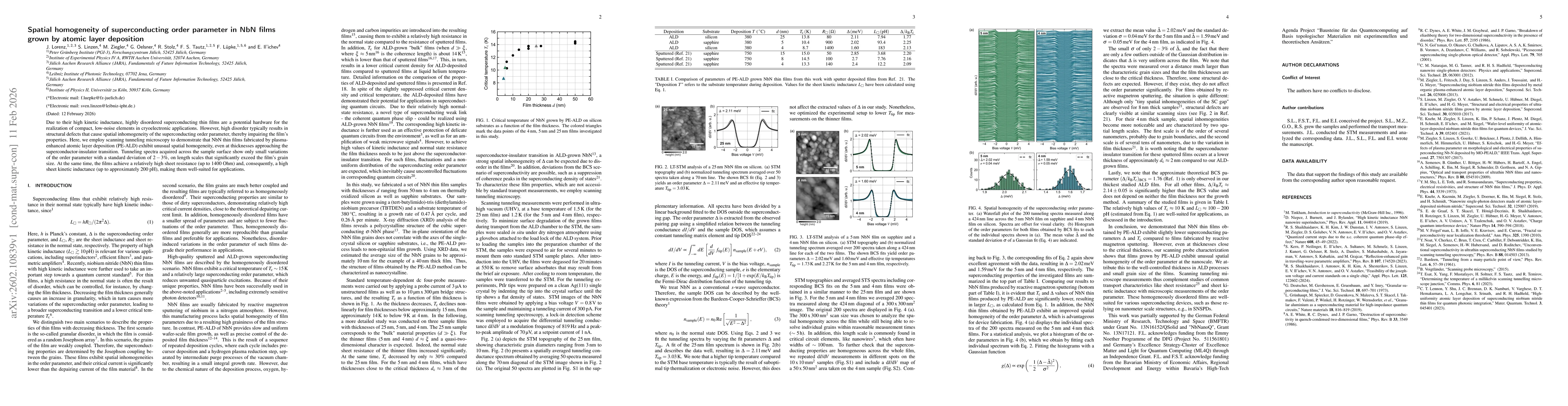
Due to their high kinetic inductance, highly disordered superconducting thin films are a potential hardware for the realization of compact, low-noise elements in cryoelectronic applications. However, ...