ArxivLens
F
Researcher

Fabian Cadiz

12 papers on arXiv

12 arXiv Papers
66 Total Publications
Profile

Academic Profile

Name F. Cadiz
Total Papers 66
Scholar Profile View on Semantic Scholar
Metrics

Statistics

12 arXiv Papers
66 Total Publications
Publications

Papers on arXiv

Thumbnail for High Strain Engineering of a Suspended WSSe Monolayer Membrane by
  Indentation and Measured by Tip-enhanced Photoluminescence
arXiv
High Strain Engineering of a Suspended WSSe Monolayer Membrane by Indentation and Measured by Tip-enhanced Photoluminescence

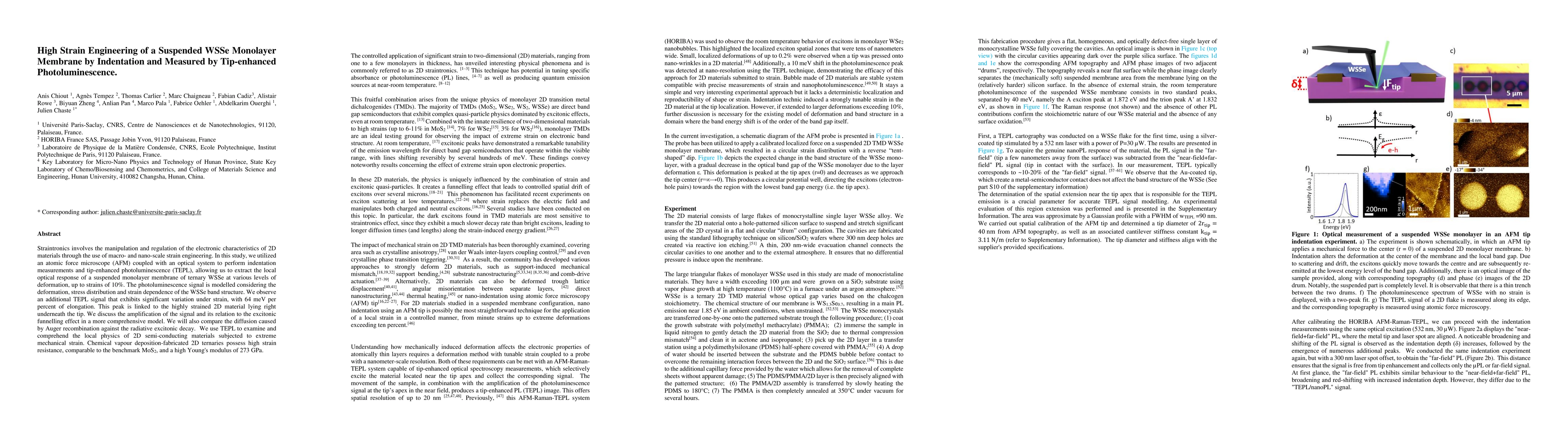
Straintronics involves the manipulation and regulation of the electronic characteristics of 2D materials through the use of macro- and nano-scale strain engineering. In this study, we utilized an at...

Thumbnail for Enhancement of valley polarization at high photoexcited densities in
  MoS2 monolayers
arXiv
Enhancement of valley polarization at high photoexcited densities in MoS2 monolayers

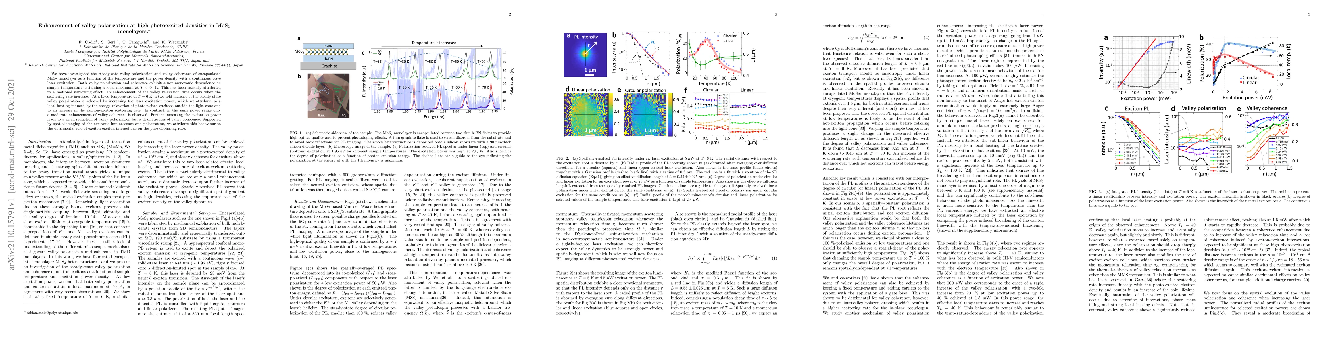
We have investigated the steady-sate valley polarization and valley coherence of encapsulated MoS2 monolayer as a function of the temperature and the power density with a continuous wave laser excit...

Thumbnail for Efficient valley polarization of charged excitons and resident carriers
  in MoS2 monolayers by optical pumping
arXiv
Efficient valley polarization of charged excitons and resident carriers in MoS2 monolayers by optical pumping

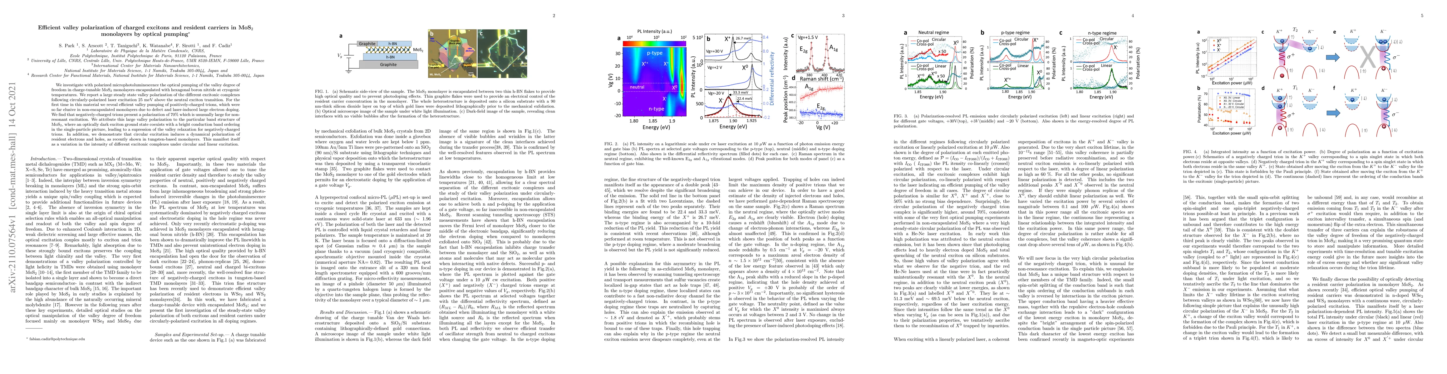
We investigate with polarized microphotoluminescence the optical pumping of the valley degree of freedom in charge-tunable MoS2 monolayers encapsulated with hexagonal boron nitride at cryogenic temp...

Thumbnail for Imaging Seebeck drift of excitons and trions in MoSe2 monolayers
arXiv
Imaging Seebeck drift of excitons and trions in MoSe2 monolayers

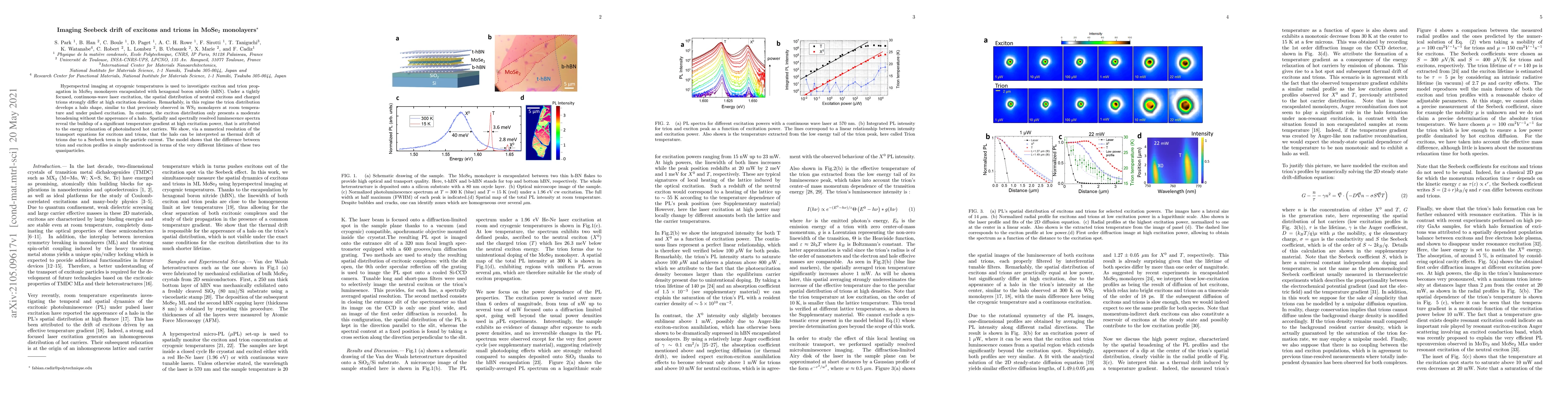
Hyperspectral imaging at cryogenic temperatures is used to investigate exciton and trion propagation in MoSe$_2$ monolayers encapsulated with hexagonal boron nitride (hBN). Under a tightly focused, ...

Thumbnail for Spin/Valley pumping of resident electrons in WSe2 and WS2 monolayers
arXiv
Spin/Valley pumping of resident electrons in WSe2 and WS2 monolayers

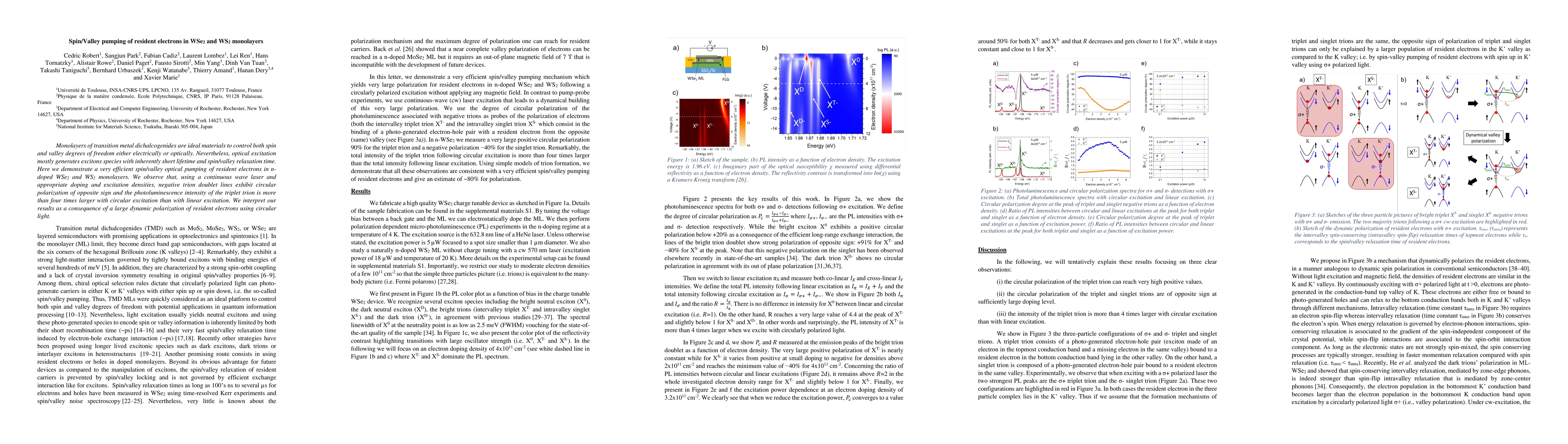
Monolayers of transition metal dichalcogenides are ideal materials to control both spin and valley degrees of freedom either electrically or optically. Nevertheless, optical excitation mostly genera...

Thumbnail for Charge and spin transport over record distances in GaAs metallic n-type
  nanowires : II nonlinear charge transport
arXiv
Charge and spin transport over record distances in GaAs metallic n-type nanowires : II nonlinear charge transport

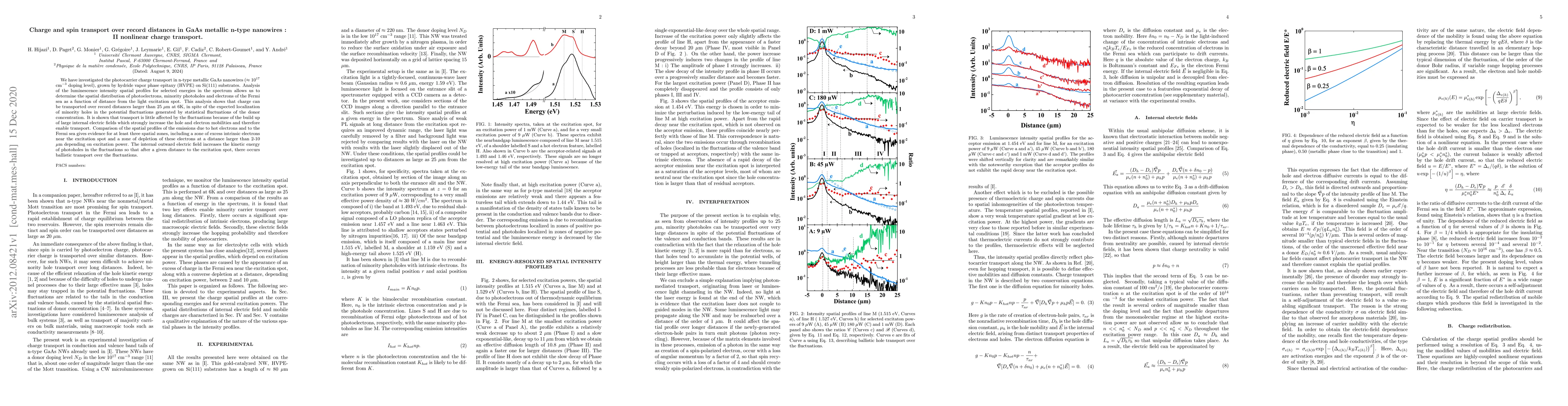
We have investigated the photocarrier charge transport in n-type metallic GaAs nanowires (~ 10^17 cm^-3 doping level), grown by hydride vapor phase epitaxy (HVPE) on Si(111) substrates. Analysis of ...

Thumbnail for Charge and spin transport over record distances in GaAs metallic n-type
  nanowires : I photocarrier transport in a dense Fermi sea
arXiv
Charge and spin transport over record distances in GaAs metallic n-type nanowires : I photocarrier transport in a dense Fermi sea

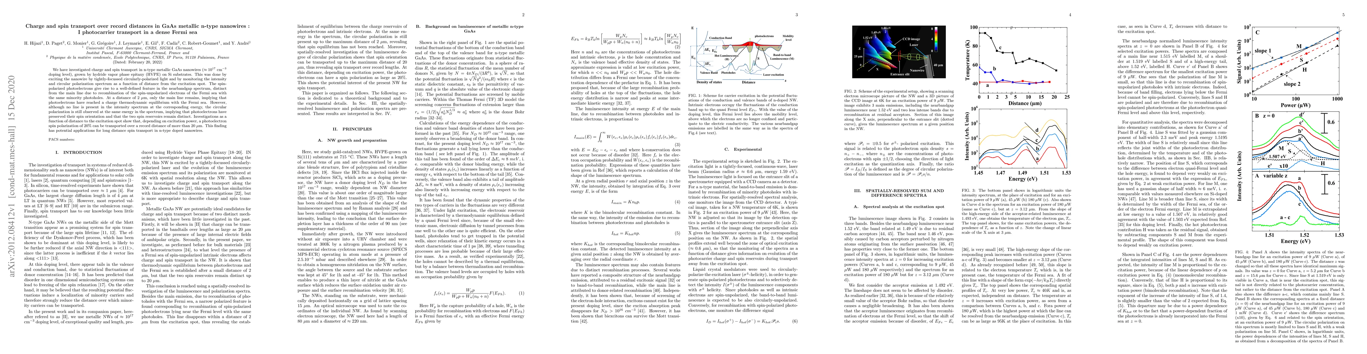
We have investigated charge and spin transport in n-type metallic GaAs nanowires (~ 10^17 cm^-3 doping level), grown by hydride vapor phase epitaxy (HVPE) on Si substrates. This was done by exciting...

Thumbnail for Electrical Detection of Light Helicity using a Quantum Dots based Hybrid
  Device at Zero Magnetic Field
arXiv
Electrical Detection of Light Helicity using a Quantum Dots based Hybrid Device at Zero Magnetic Field

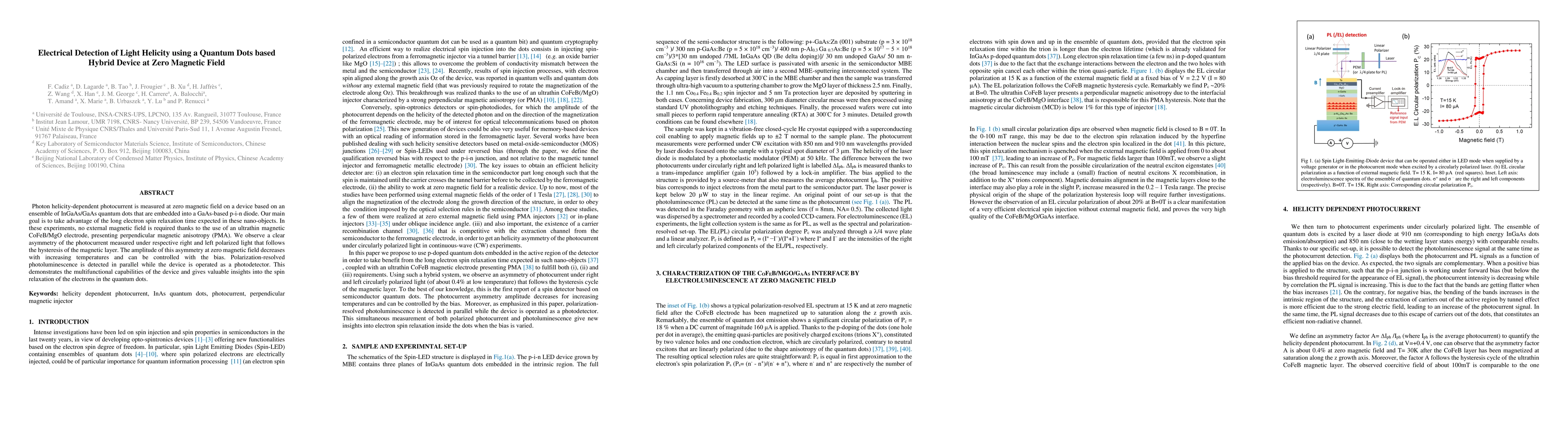
Photon helicity-dependent photocurrent is measured at zero magnetic field on a device based on an ensemble of InGaAs/GaAs quantum dots that are embedded into a GaAs-based p-i-n diode. Our main goal ...

Thumbnail for Using Light to Polarize and Detect Electron Spins in Silicon
arXiv
Using Light to Polarize and Detect Electron Spins in Silicon

Despite decades of research, demonstration of all-optical detection and control of free electron spins in silicon remains elusive. Here, we directly probe the electron spin properties in bulk silicon ...

Thumbnail for Crystal field tuned spin-flip luminescence in NiPS3
arXiv
Crystal field tuned spin-flip luminescence in NiPS3

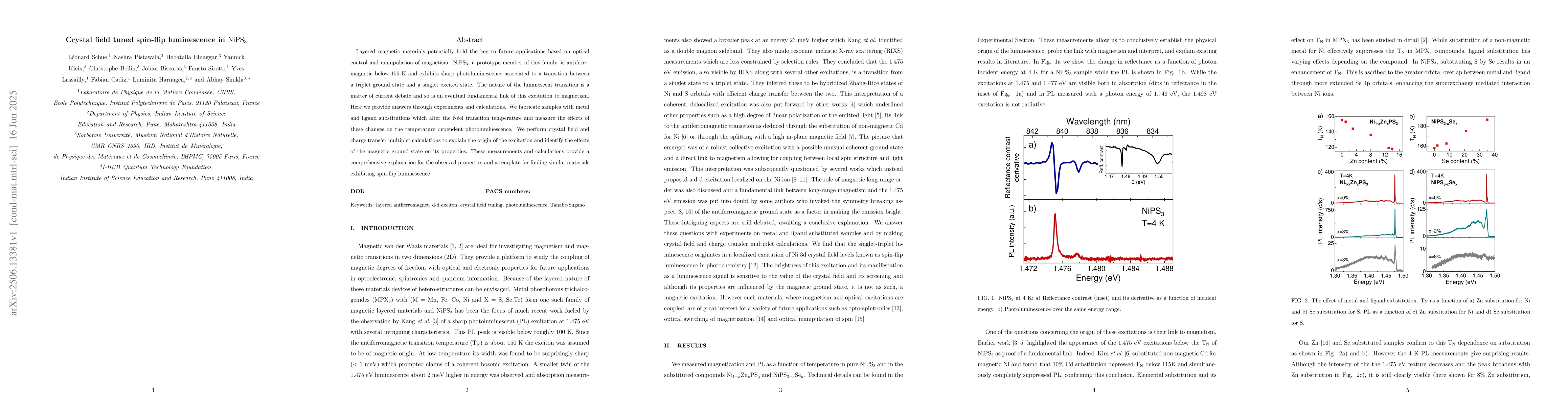
Layered magnetic materials potentially hold the key to future applications based on optical control and manipulation of magnetism. NiPS3, a prototype member of this family, is antiferromagnetic below ...

Thumbnail for Tunable electronic band structure in WSSe van der Waals Alloys
arXiv
Tunable electronic band structure in WSSe van der Waals Alloys

The electronic structure of semiconducting 2D materials such as transition metal dichalcogenides (TMDs) is known to be tunable by its environment, from simple external fields applied with electrical c...

Thumbnail for High-Temperature Activation of Single-Photon Emitters in monolayer WS2
arXiv
High-Temperature Activation of Single-Photon Emitters in monolayer WS2

Controlled activation of defect-bound excitonic states in two-dimensional semiconductors provides a route to isolated quantum emitters and a sensitive probe of defect physics. Here we demonstrate that...

This website uses cookies to ensure you get the best experience. Learn more