Academic Profile
Statistics
Similar Authors
Papers on arXiv
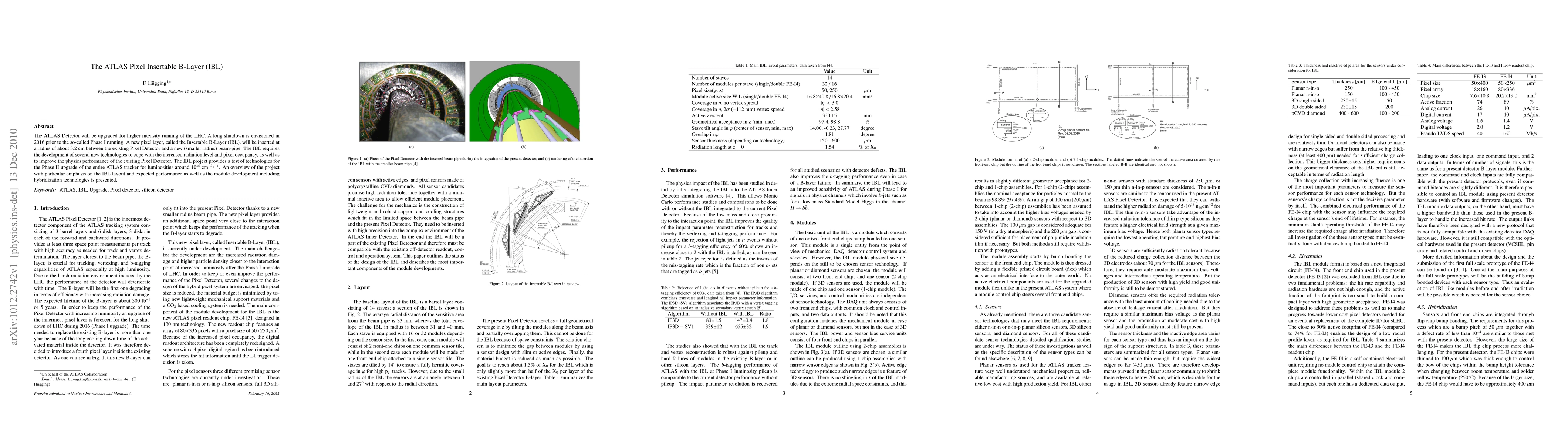
The ATLAS Detector will be upgraded for higher intensity running of the LHC. A long shutdown is envisioned in 2016 prior to the so-called Phase I running. A new pixel layer, called the Insertable B-...
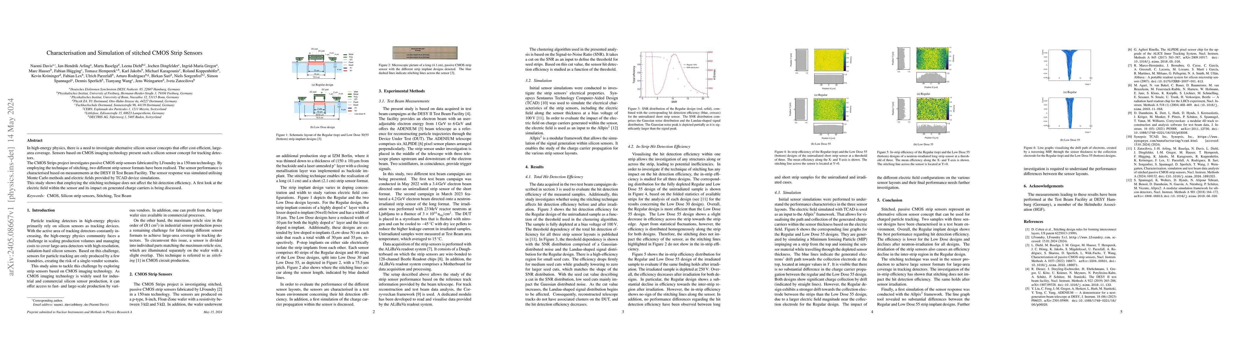
In high-energy physics, there is a need to investigate alternative silicon sensor concepts that offer cost-efficient, large-area coverage. Sensors based on CMOS imaging technology present such a sil...
Monolithic pixel detectors combine readout electronics and sensor in a single entity of silicon, which simplifies the production procedure and lowers the material budget compared to conventional hyb...
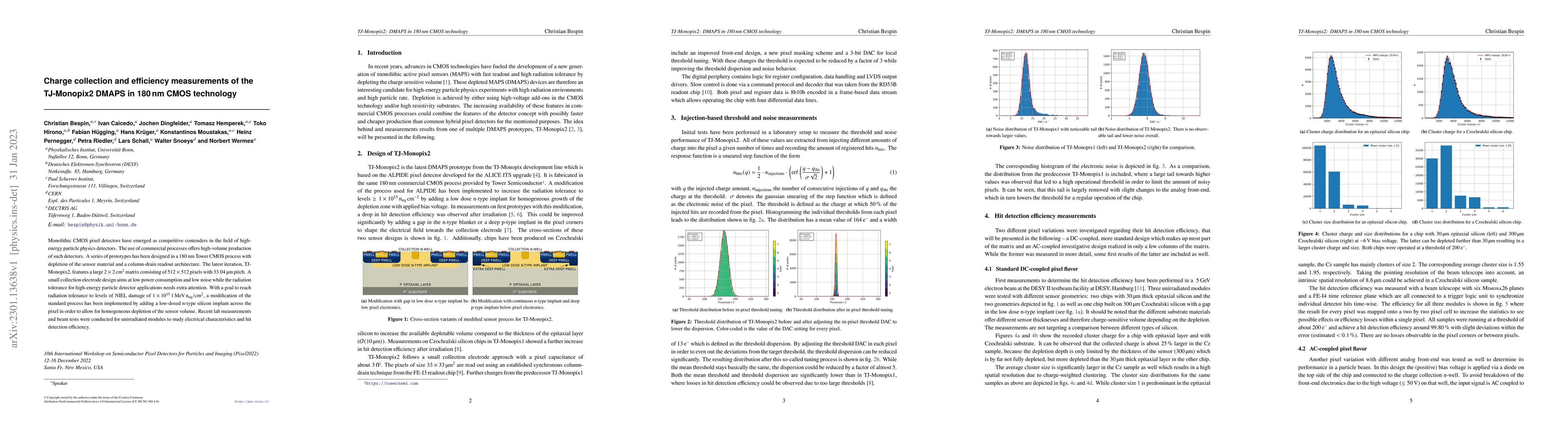
Monolithic CMOS pixel detectors have emerged as competitive contenders in the field of high-energy particle physics detectors. By utilizing commercial processes they offer high-volume production of ...
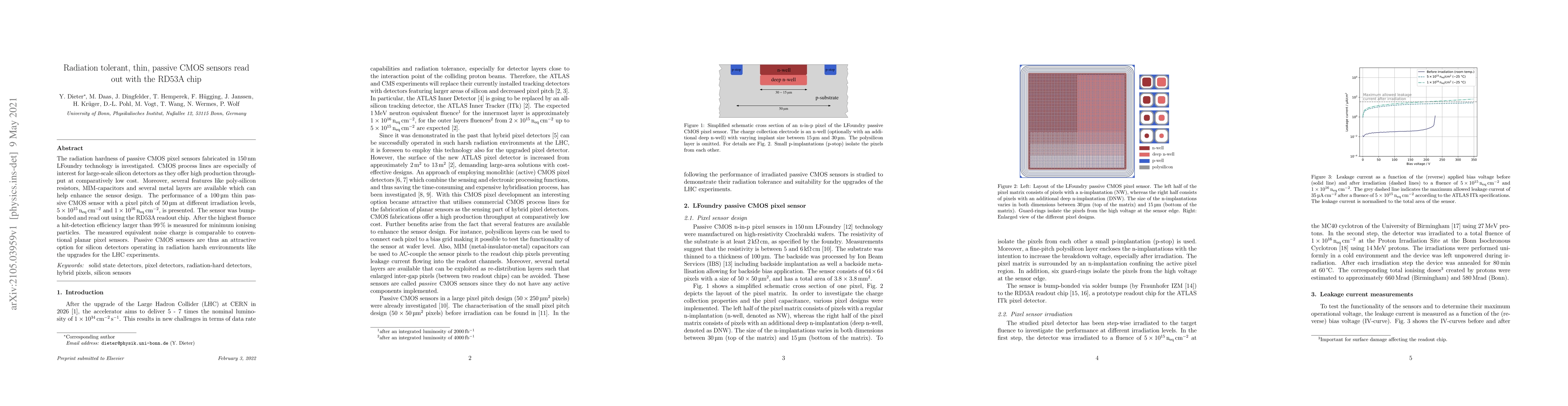
The radiation hardness of passive CMOS pixel sensors fabricated in 150 nm LFoundry technology is investigated. CMOS process lines are especially of interest for large-scale silicon detectors as they...
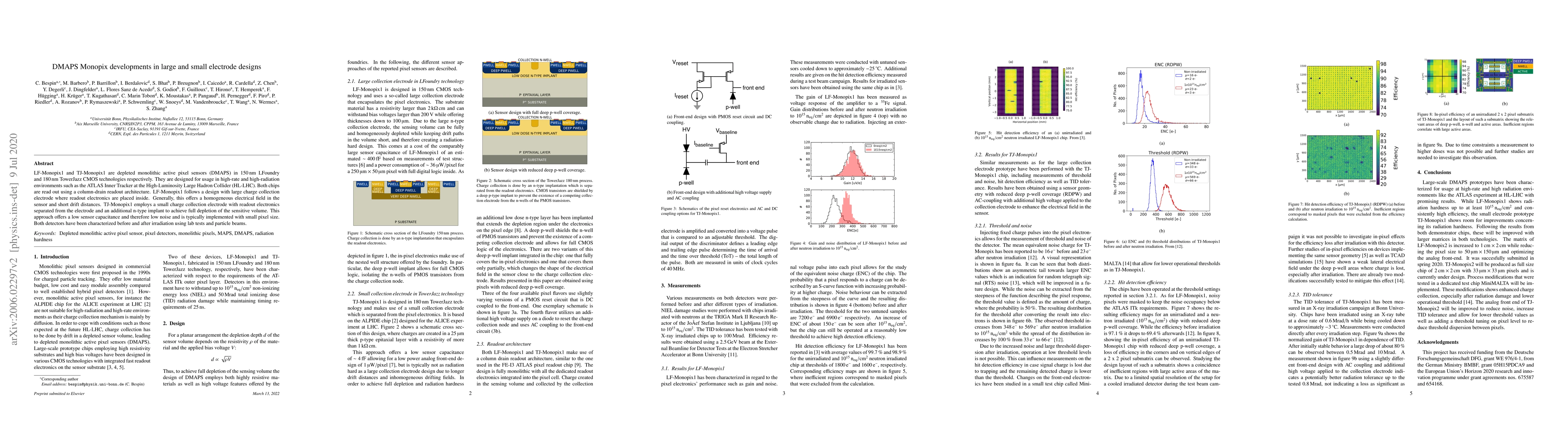
LF-Monopix1 and TJ-Monopix1 are depleted monolithic active pixel sensors (DMAPS) in 150 nm LFoundry and 180 nm TowerJazz CMOS technologies respectively. They are designed for usage in high-rate and ...
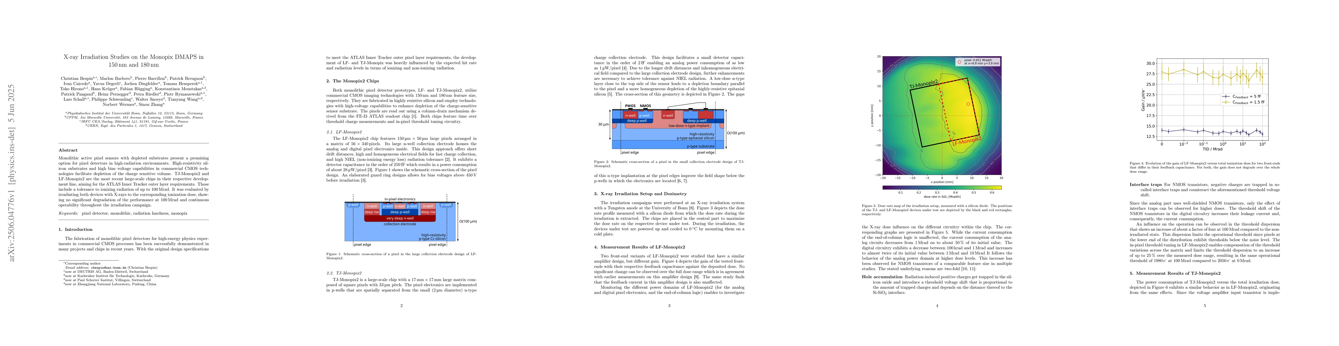
Monolithic active pixel sensors with depleted substrates present a promising option for pixel detectors in high-radiation environments. High-resistivity silicon substrates and high bias voltage capabi...
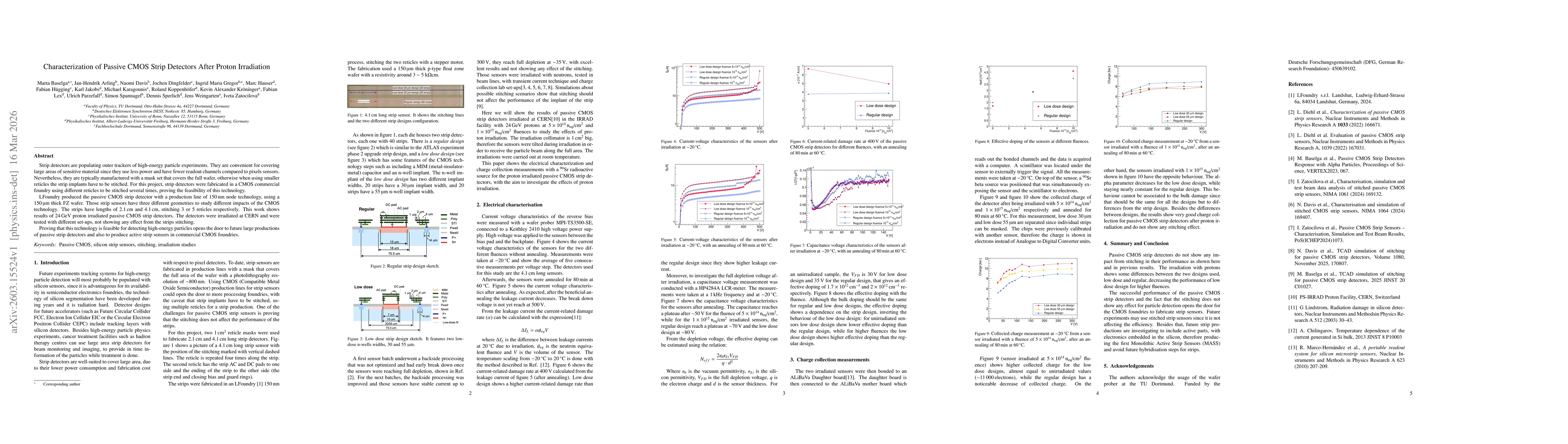
Strip detectors are populating outer trackers of high-energy particle experiments. They are convenient for covering large areas of sensitive material since they use less power and have fewer readout c...
Semiconductor pixel detectors are widely established in High Energy Physics (HEP) and Medical physics for their high spatial resolution and tracking capabilities. Research on both monolithic detectors...