Academic Profile
Statistics
Similar Authors
Papers on arXiv
Resonant transport is demonstrated in a hybrid superconductor-semiconductor heterostructure junction grown by molecular beam epitaxy on GaAs. This heterostructure realizes the model system introduce...
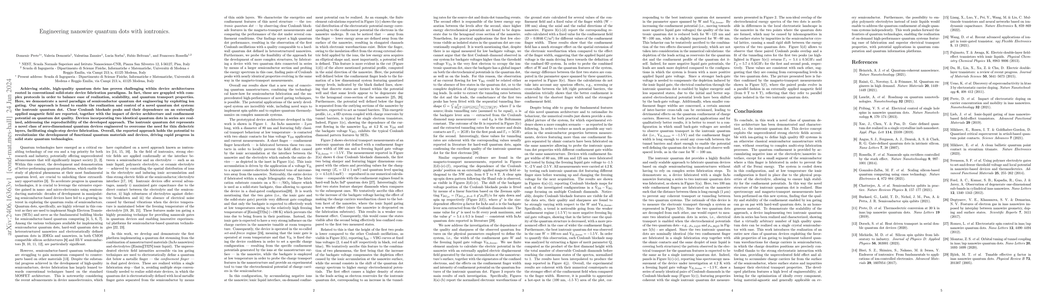
Achieving stable, high-quality quantum dots has proven challenging within device architectures rooted in conventional solid-state device fabrication paradigms. In fact, these are grappled with compl...
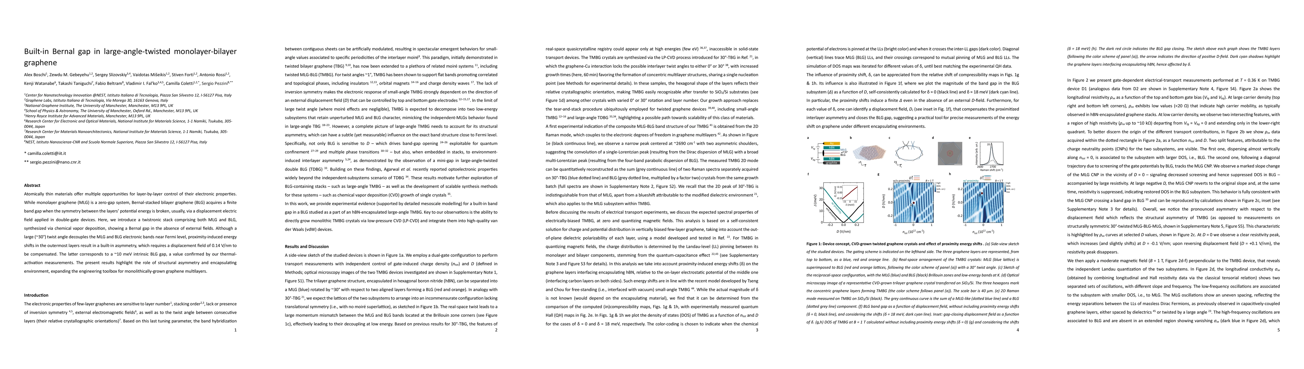
Atomically thin materials offer multiple opportunities for layer-by-layer control of their electronic properties. While monolayer graphene (MLG) is a zero-gap system, Bernal-stacked bilayer graphene...
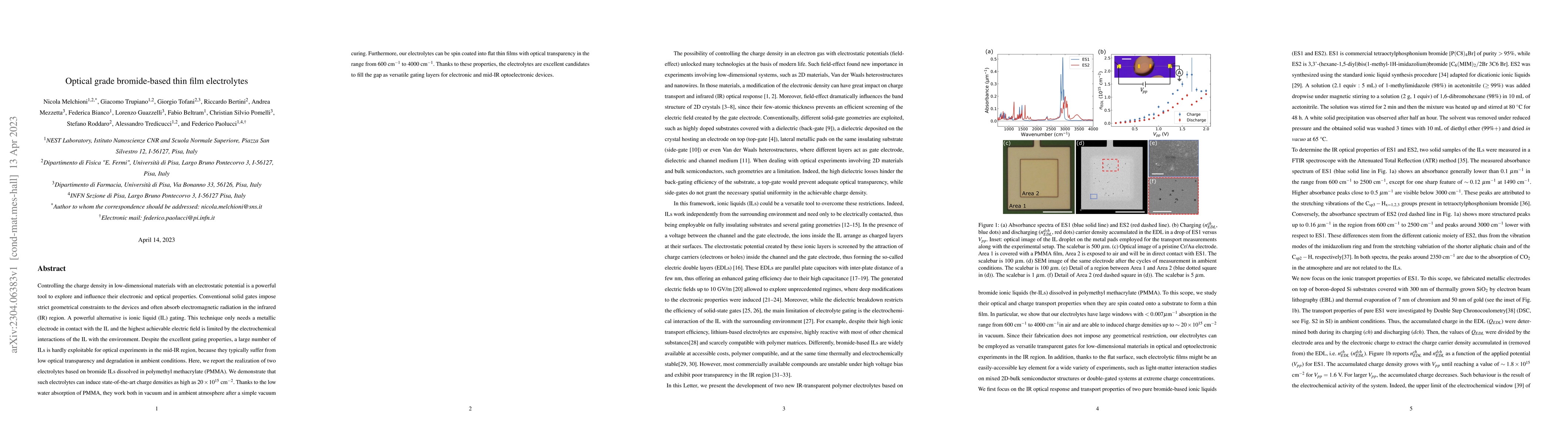
Controlling the charge density in low-dimensional materials with an electrostatic potential is a powerful tool to explore and influence their electronic and optical properties. Conventional solid ga...
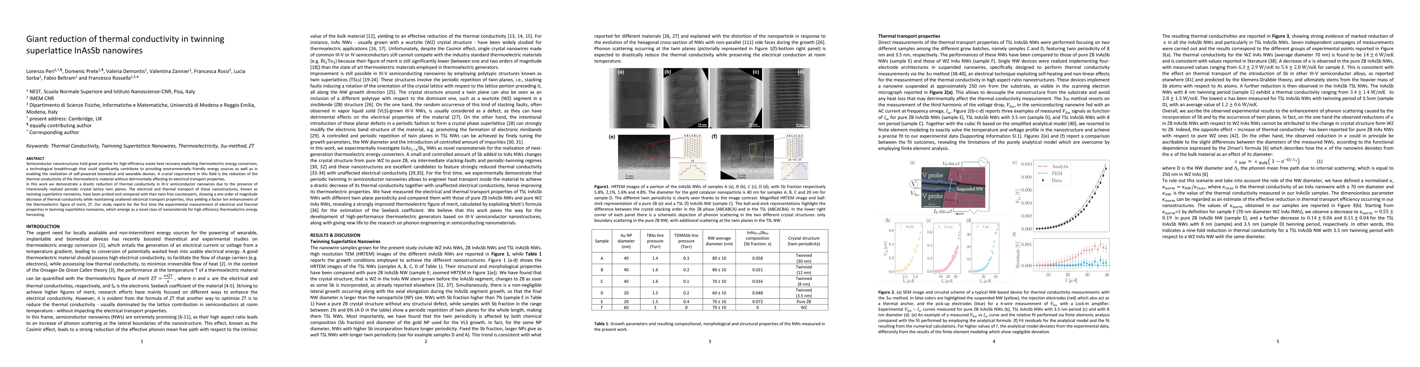
Semiconductor nanostructures hold great promise for high-efficiency waste heat recovery exploiting thermoelectric energy conversion, a technological breakthrough that could significantly contribute ...
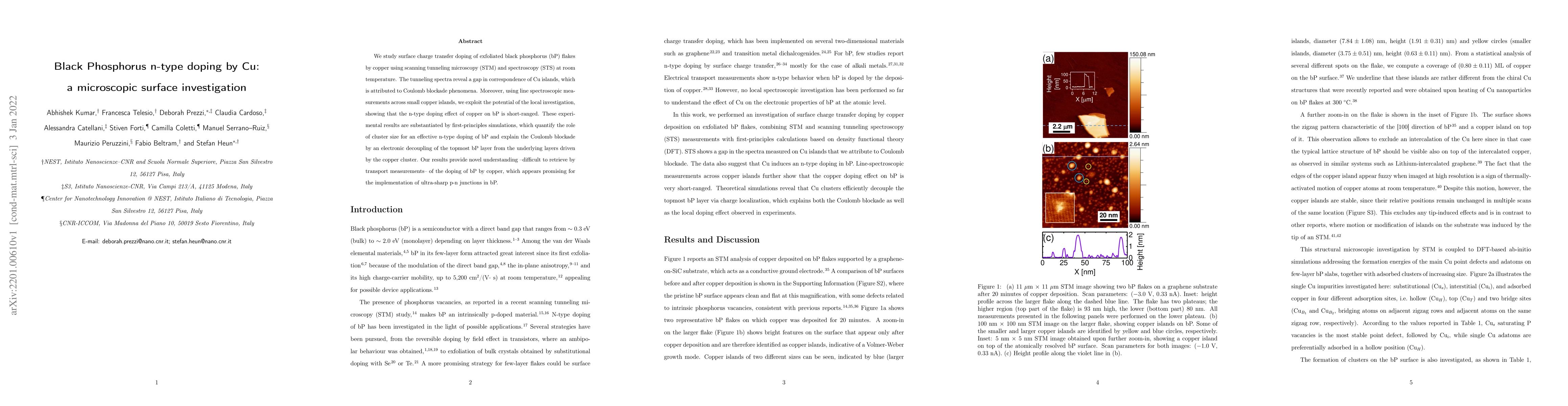
We study surface charge transfer doping of exfoliated black phosphorus (bP) flakes by copper using scanning tunneling microscopy (STM) and spectroscopy (STS) at room temperature. The tunneling spect...
High quality heteroepitaxial two-dimensional (2D) InSb layers are very difficult to realize owing to the large lattice mismatch with other widespread semiconductor substrates. A way around this prob...
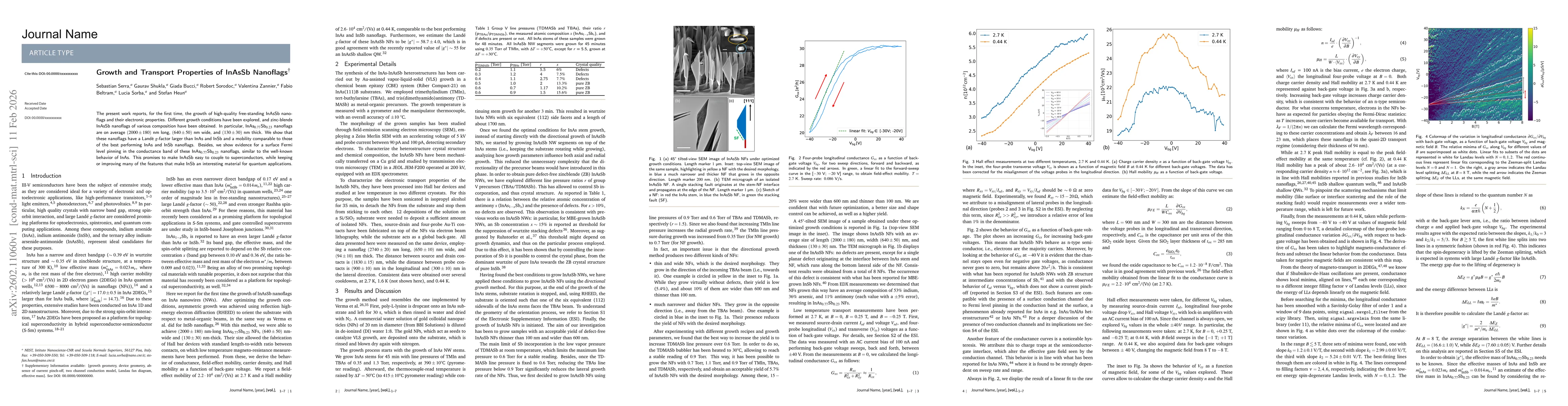
High-quality III-V narrow band gap semiconductor materials with strong spin-orbit coupling and large Lande g-factor provide a promising platform for next-generation applications in the field of high...
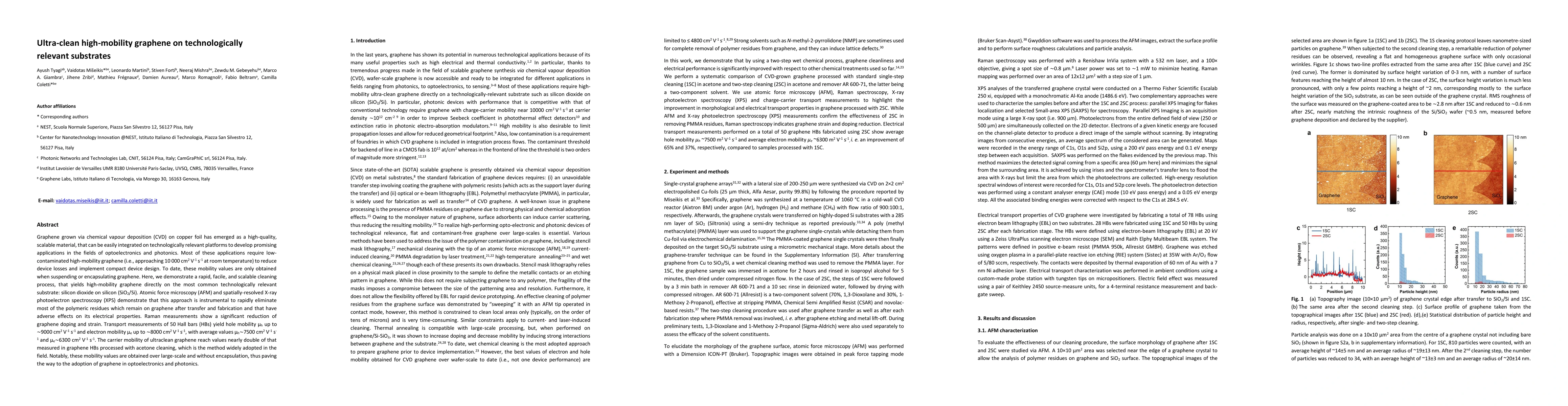
Graphene grown via chemical vapour deposition (CVD) on copper foil has emerged as a high-quality, scalable material, that can be easily integrated on technologically relevant platforms to develop pr...
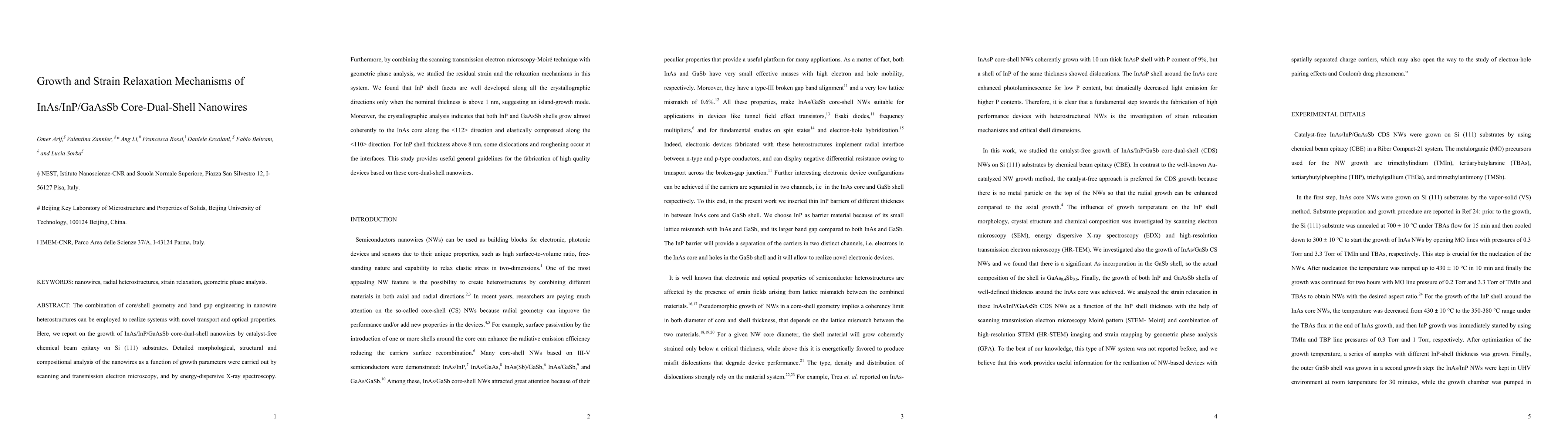
The combination of core/shell geometry and band gap engineering in nanowire heterostructures can be employed to realize systems with novel transport and optical properties. Here, we report on the gr...
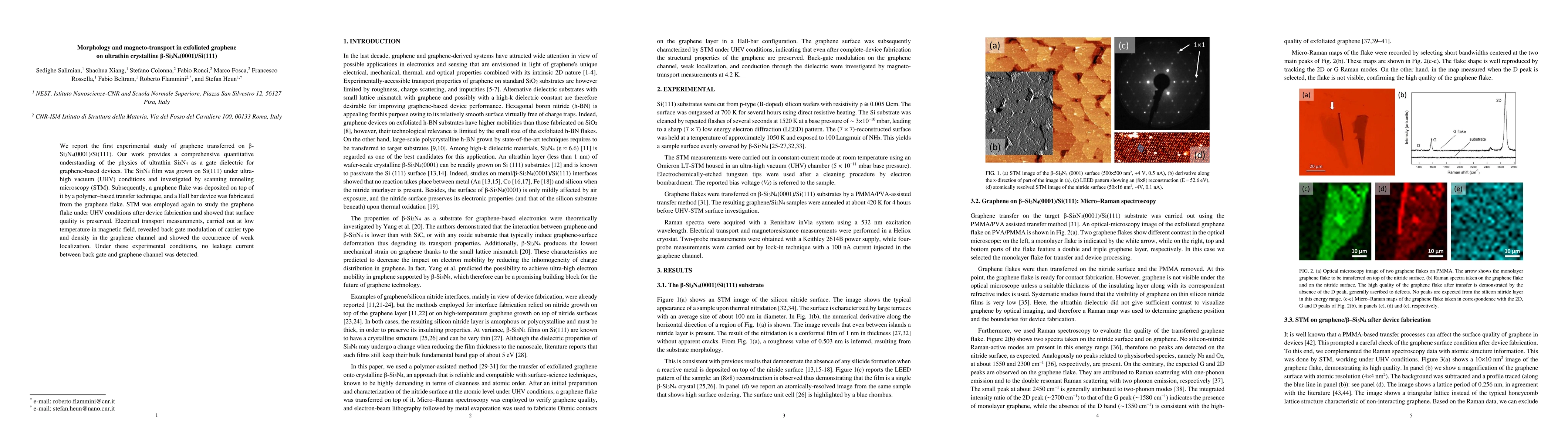
We report the first experimental study of graphene transferred on \b{eta}-Si3N4(0001)/Si(111). Our work provides a comprehensive quantitative understanding of the physics of ultrathin Si3N4 as a gat...
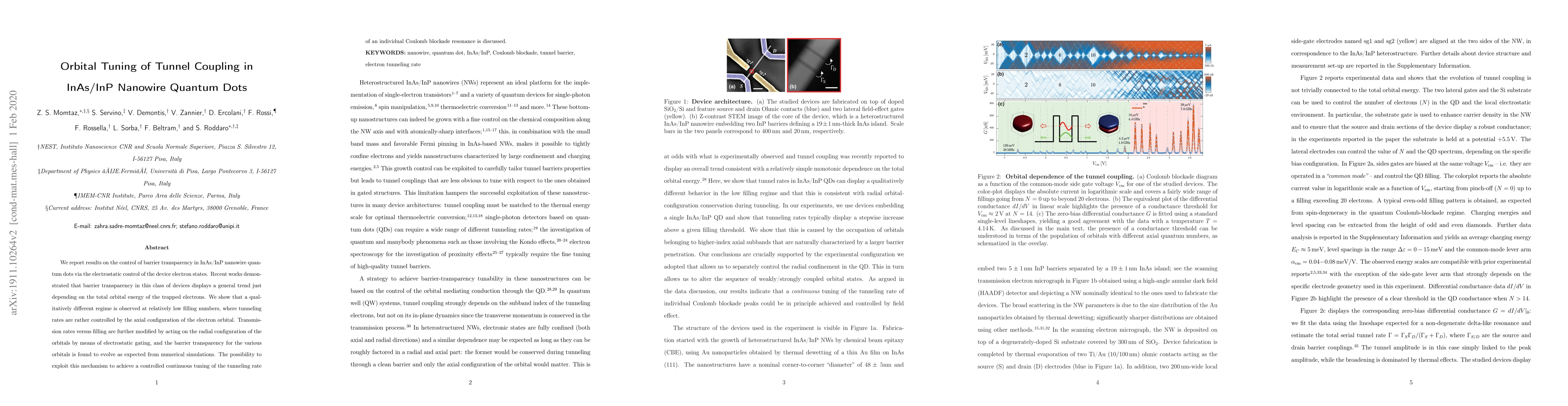
We report results on the control of barrier transparency in InAs/InP nanowire quantum dots via the electrostatic control of the device electron states. Recent works demonstrated that barrier transpa...
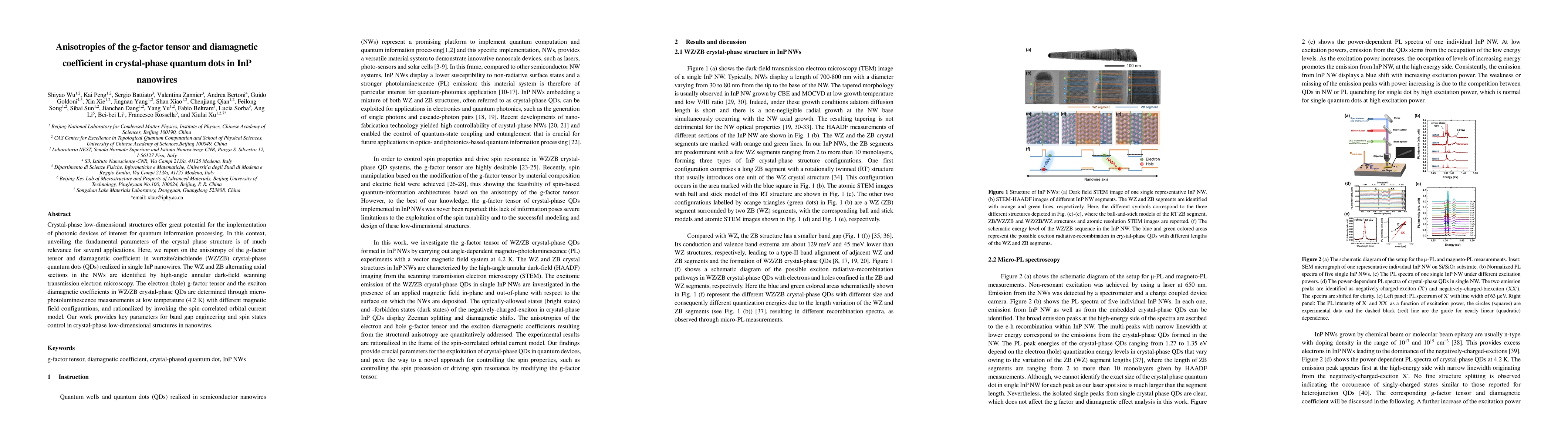
Crystal-phase low-dimensional structures offer great potential for the implementation of photonic devices of interest for quantum information processing. In this context, unveiling the fundamental p...
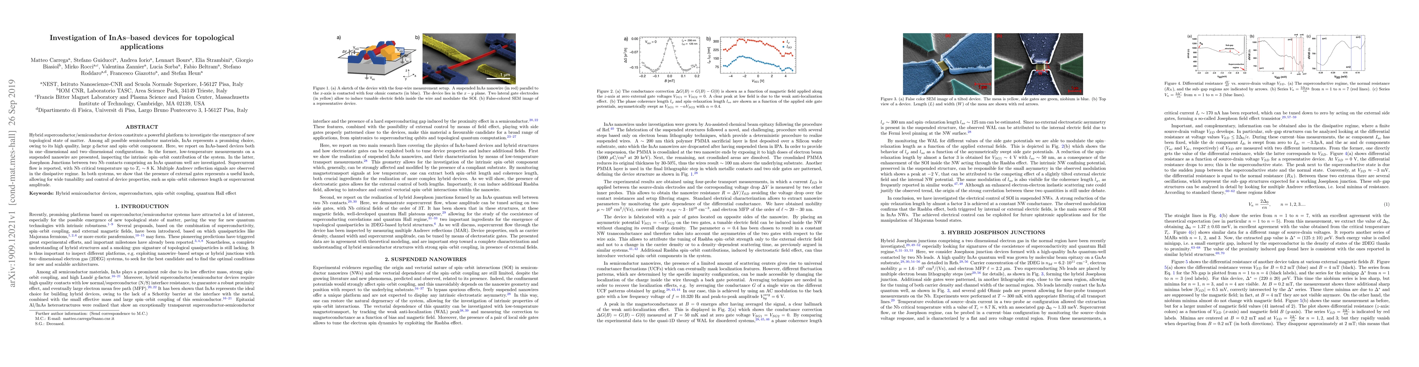
Hybrid superconductor/semiconductor devices constitute a powerful platform to investigate the emergence of new topological state of matter. Among all possible semiconductor materials, InAs represent...
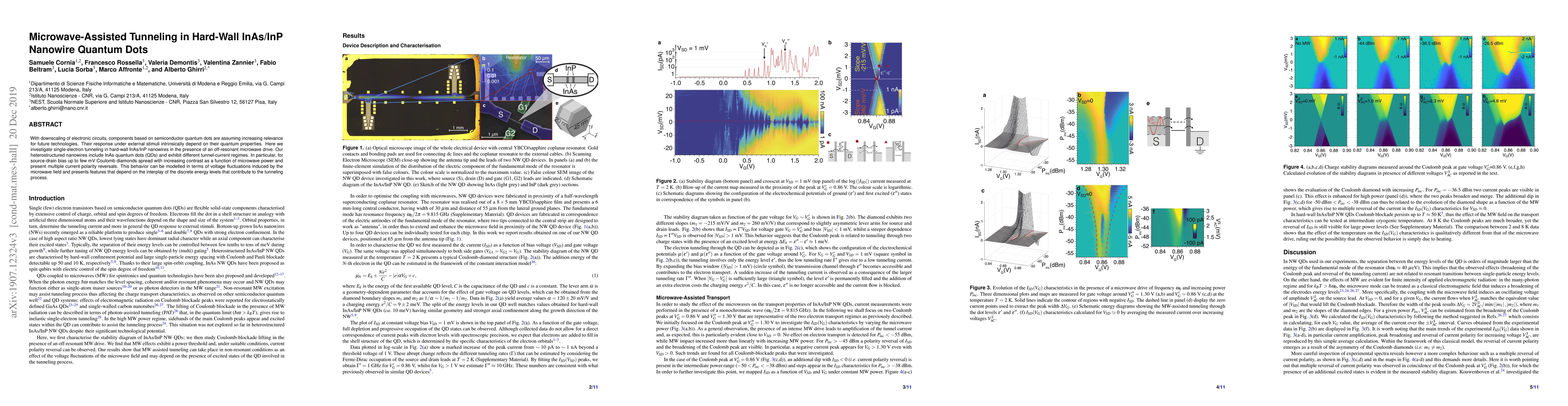
With downscaling of electronic circuits, components based on semiconductor quantum dots are assuming increasing relevance for future technologies. Their response under external stimuli intrinsically...

Two-dimensional (2D) materials are poised to revolutionize current solid-state technology with their extraordinary properties. Yet, the primary challenge remains their scalable production. While there...
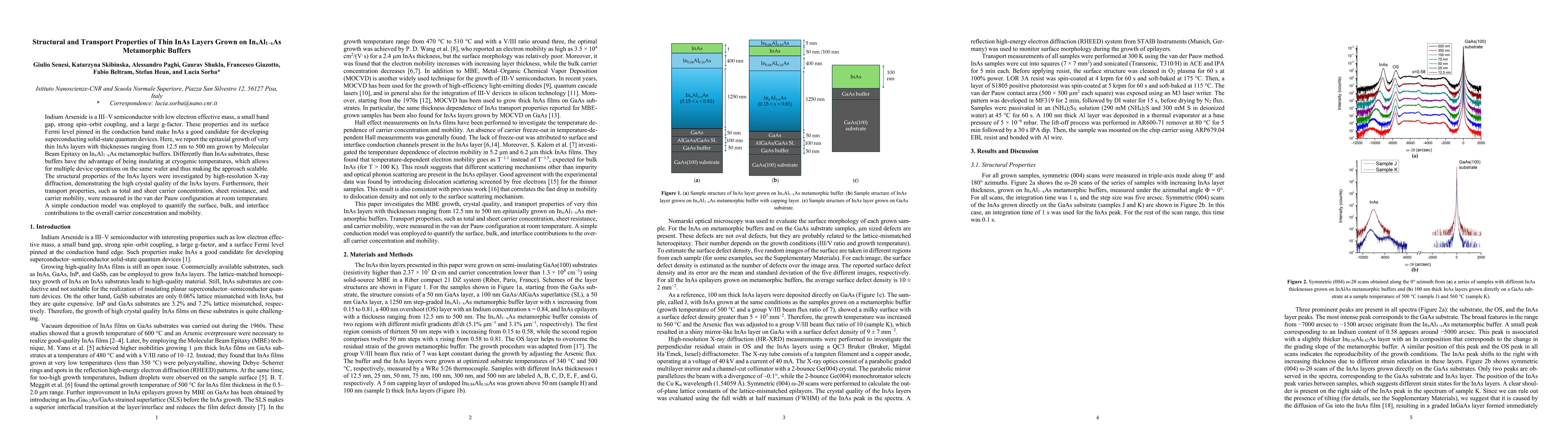
Indium Arsenide is a III-V semiconductor with low electron effective mass, a small band gap, strong spin-orbit coupling, and a large g-factor. These properties and its surface Fermi level pinned in th...
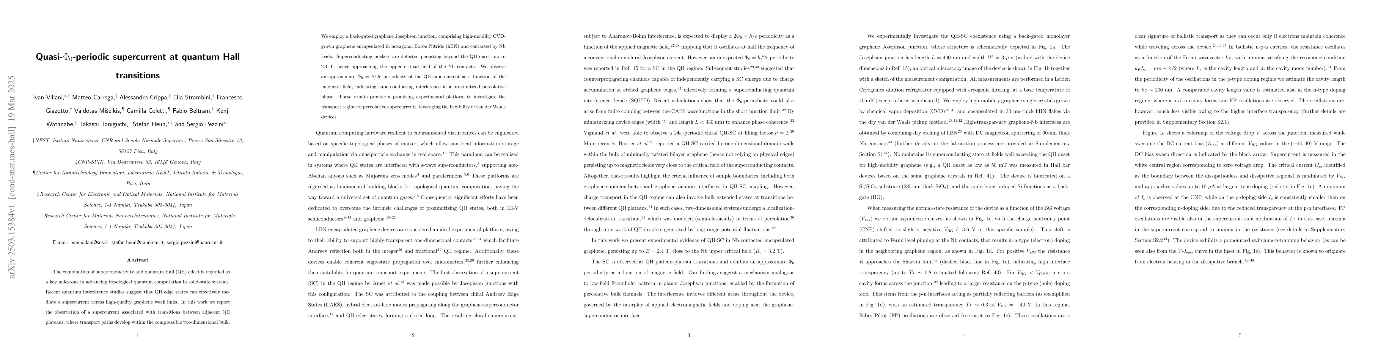
The combination of superconductivity and quantum Hall (QH) effect is regarded as a key milestone in advancing topological quantum computation in solid-state systems. Recent quantum interference studie...
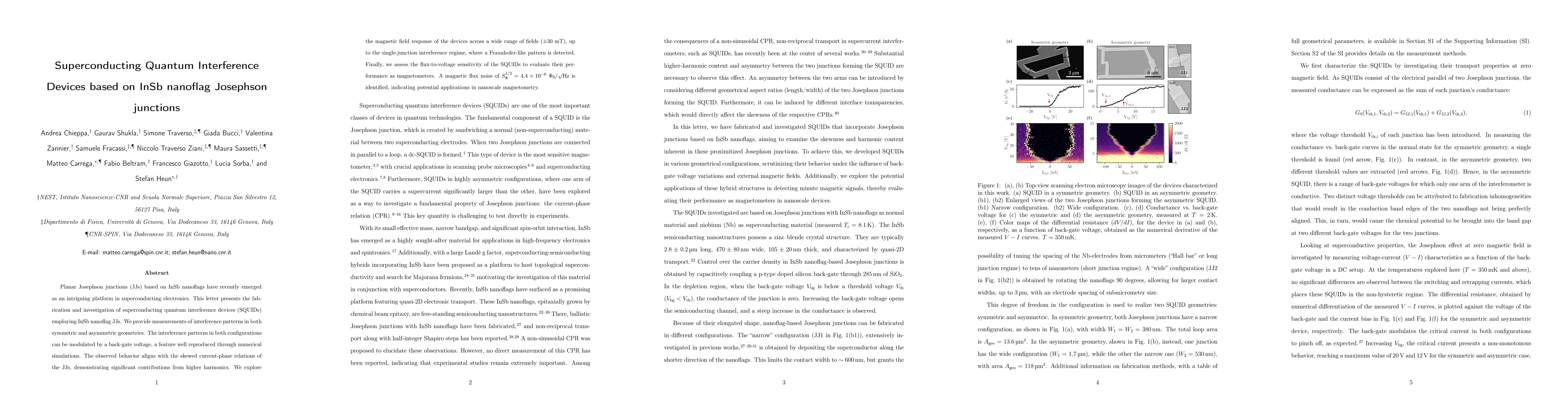
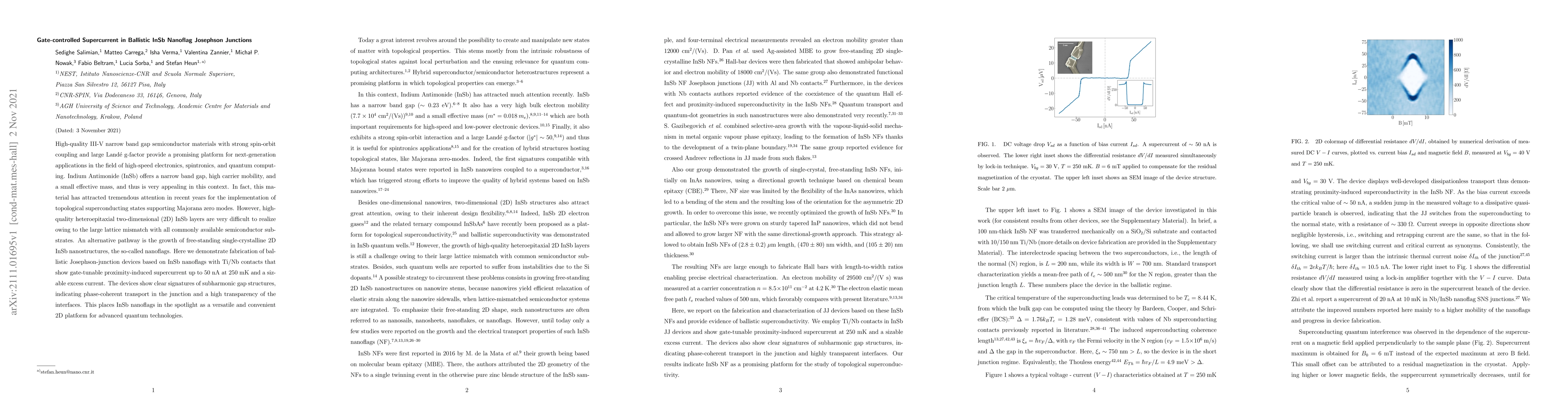
Planar Josephson junctions (JJs) based on InSb nanoflags have recently emerged as an intriguing platform in superconducting electronics. This letter presents the fabrication and investigation of super...
The creation of atomically thin layers of non-exfoliable materials remains a crucial challenge, requiring the development of innovative techniques. Here, confinement epitaxy is exploited to realize tw...
InSb nanoflags represent an interesting platform for quantum transport and have recently been exploited in the study of hybrid planar Josephson junctions. Due to the uncovered semiconductor surface, t...
Fine-tuning the functional properties of nanomaterials is crucial for technological applications. Superlattices, characterized by periodic repetitions of two or more materials in different dimensions,...
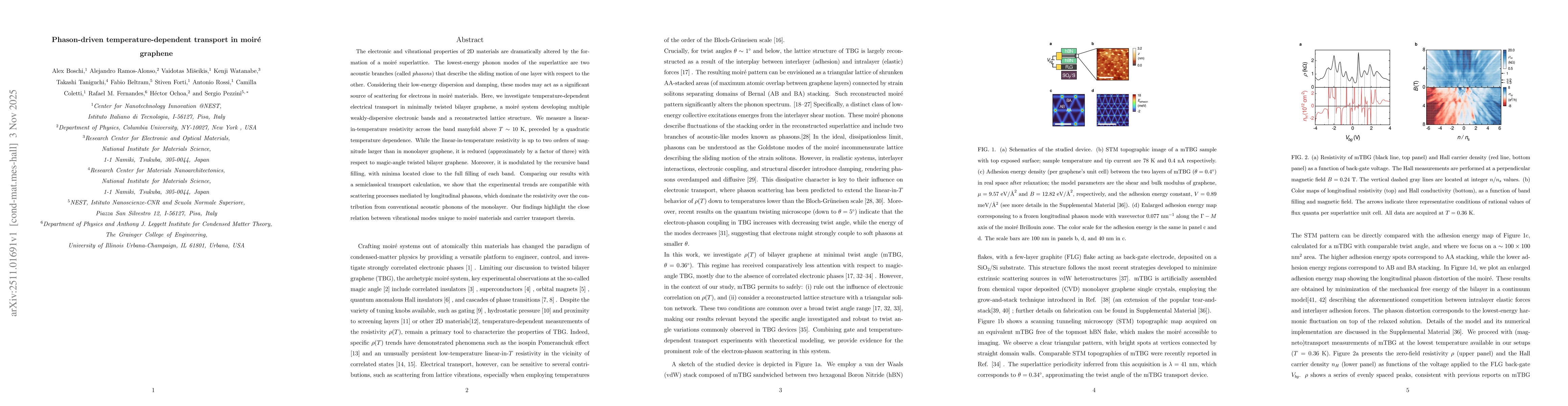
The electronic and vibrational properties of 2D materials are dramatically altered by the formation of a moiré superlattice. The lowest-energy phonon modes of the superlattice are two acoustic branche...
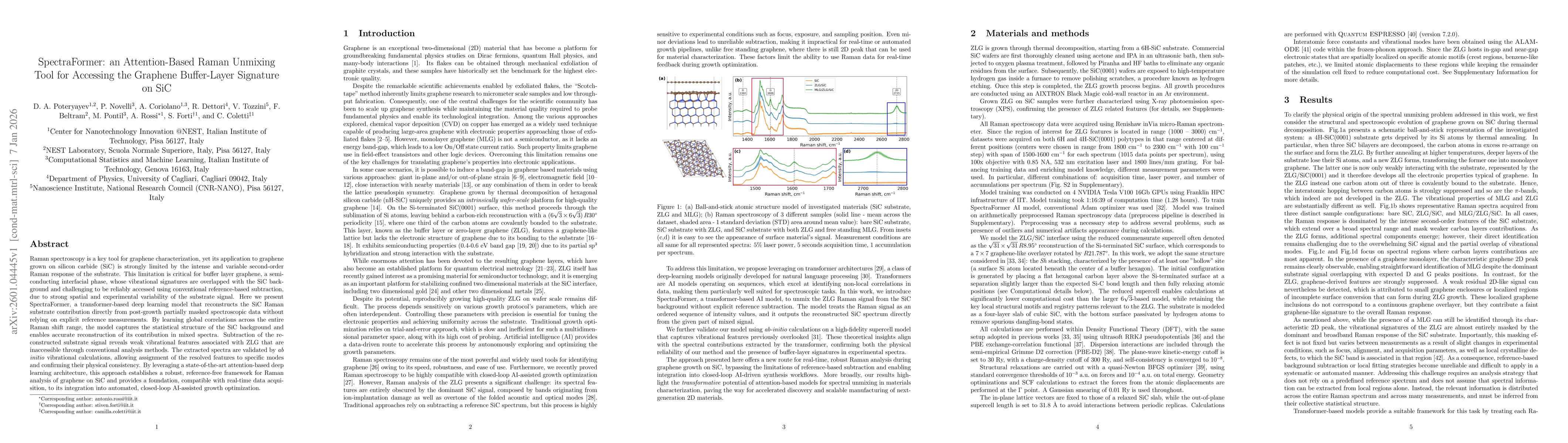
Raman spectroscopy is a key tool for graphene characterization, yet its application to graphene grown on silicon carbide (SiC) is strongly limited by the intense and variable second-order Raman respon...
The present work reports, for the first time, the growth of high-quality free-standing InAsSb nanoflags and their electronic properties. Different growth conditions have been explored, and zinc-blende...
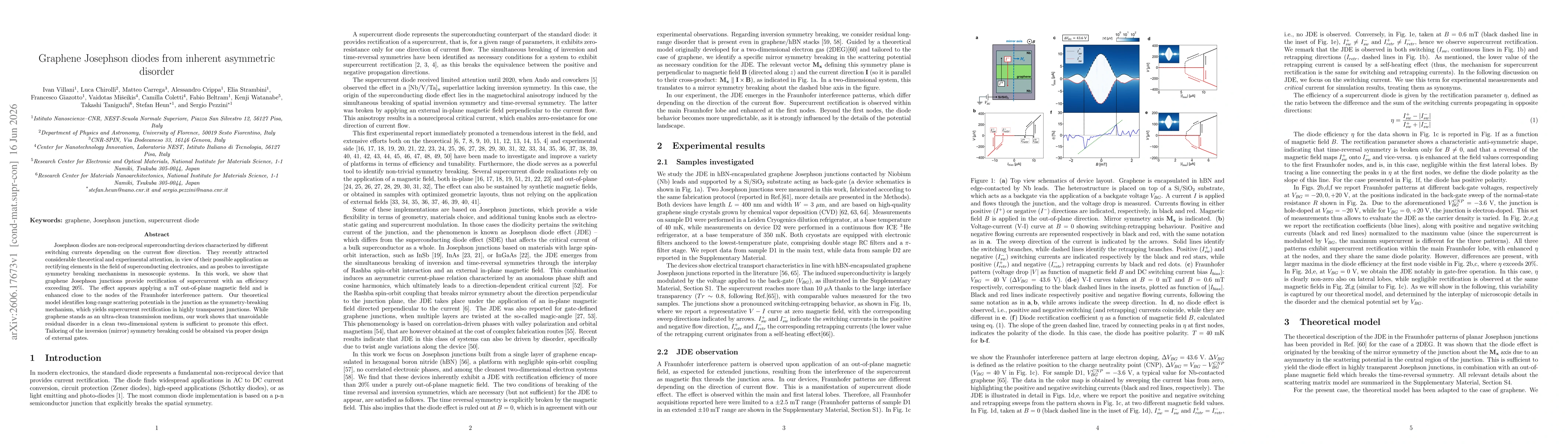
Josephson diodes are non-reciprocal superconducting devices characterized by different switching currents depending on the current flow direction. They recently attracted considerable theoretical and ...