Fabrizio Roccaforte

13 papers on arXiv

Academic Profile

Name: F. Roccaforte
Total Papers: 399

Statistics

arXiv Papers 13
Total Publications 399

Papers on arXiv

Thumbnail for Current transport in Ni Schottky barrier on GaN epilayer grown on free
  standing substrates

Current transport in Ni Schottky barrier on GaN epilayer grown on free standing substrates

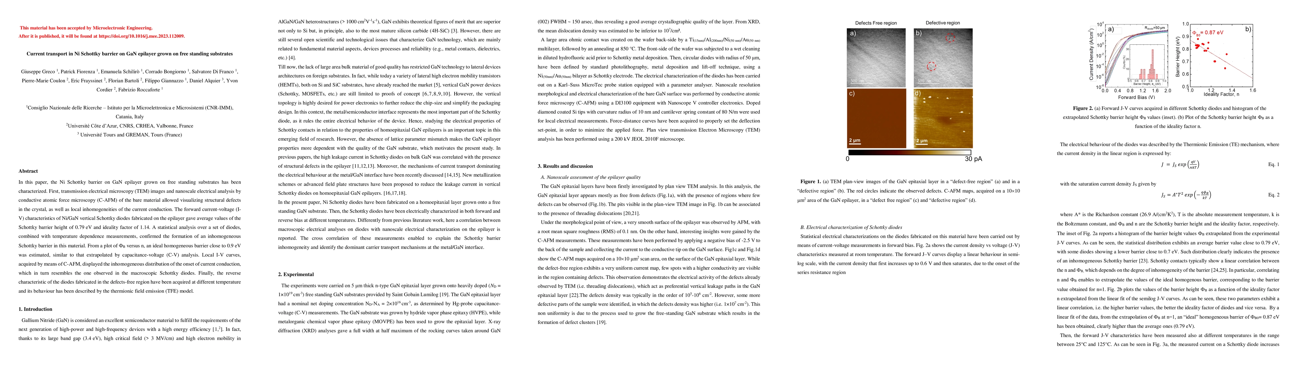
In this paper, the Ni Schottky barrier on GaN epilayer grown on free standing substrates has been characterized. First, transmission electrical microscopy (TEM) images and nanoscale electrical analy...

Thumbnail for Threshold voltage instability by charge trapping effects in the gate
  region of p-GaN HEMTs

Threshold voltage instability by charge trapping effects in the gate region of p-GaN HEMTs

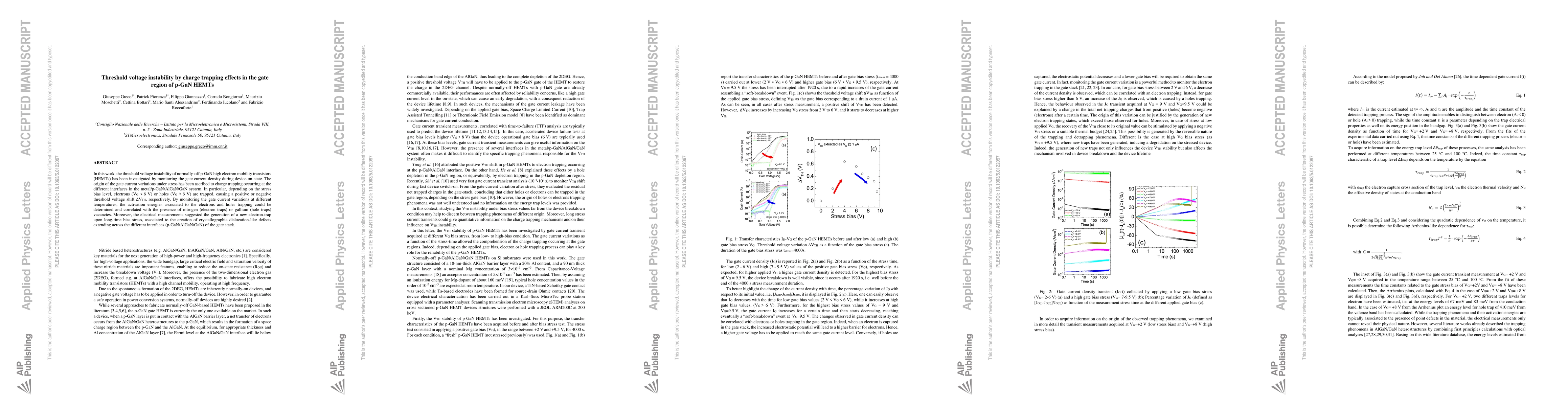
In this work, the threshold voltage instability of normally-off p-GaN high electron mobility transistors (HEMTs) has been investigated by monitoring the gate current density during device on-state. ...

Thumbnail for Electrical evolution of W and WC Schottky contacts on 4H-SiC at
  different annealing temperatures

Electrical evolution of W and WC Schottky contacts on 4H-SiC at different annealing temperatures

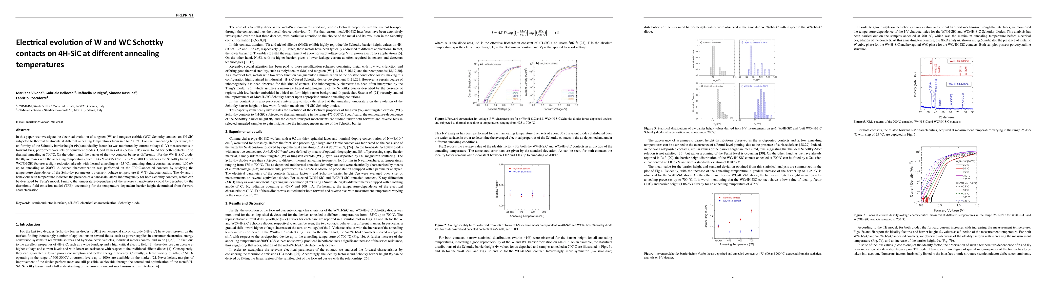
In this paper, we investigate the electrical evolution of tungsten (W) and tungsten carbide (WC) Schottky contacts on 4H-SiC subjected to thermal treatments at different annealing temperatures from ...

Thumbnail for Direct atomic layer deposition of ultrathin aluminium oxide on monolayer
  $MoS_2$ exfoliated on gold: the role of the substrate

Direct atomic layer deposition of ultrathin aluminium oxide on monolayer $MoS_2$ exfoliated on gold: the role of the substrate

In this paper we demonstrated the thermal Atomic Layer Deposition (ALD) growth at 250 {\deg}C of highly homogeneous and ultra-thin ($\approx$ 3.6 nm) $Al_2O_3$ films with excellent insulating proper...

Thumbnail for Ni Schottky barrier on heavily doped phosphorous implanted 4H-SiC

Ni Schottky barrier on heavily doped phosphorous implanted 4H-SiC

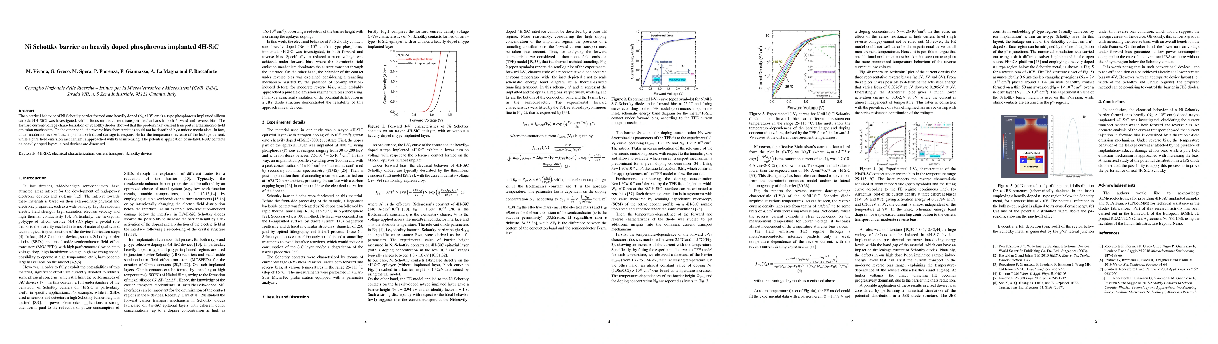
The electrical behavior of Ni Schottky barrier formed onto heavily doped (ND>1019 cm-3) n-type phosphorous implanted silicon carbide (4H-SiC) was investigated, with a focus on the current transport ...

Thumbnail for Thermal Annealing Effect on Electrical and Structural Properties of
  Tungsten Carbide Schottky Contacts on AlGaN/GaN heterostructures

Thermal Annealing Effect on Electrical and Structural Properties of Tungsten Carbide Schottky Contacts on AlGaN/GaN heterostructures

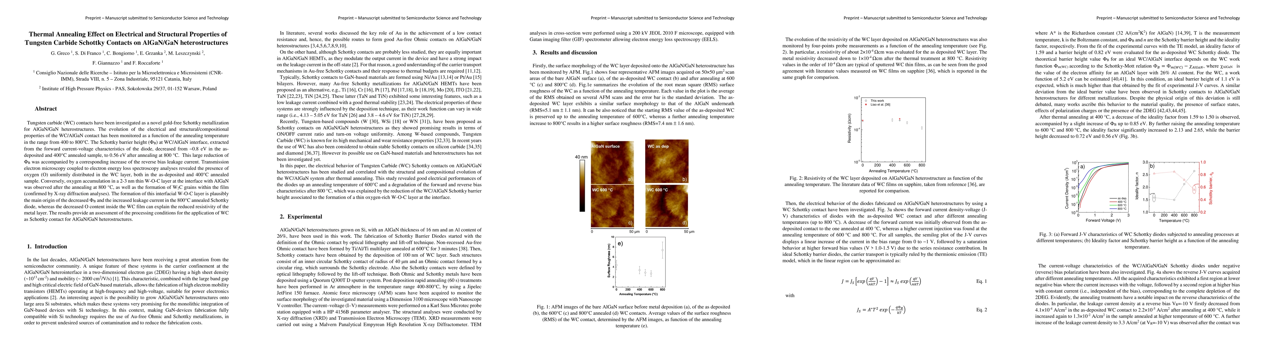
Tungsten carbide (WC) contacts have been investigated as a novel gold-free Schottky metallization for AlGaN/GaN heterostructures. The evolution of the electrical and structural/compositional propert...

Thumbnail for Electrical properties of inhomogeneous tungsten carbide Schottky barrier
  on 4H-SiC

Electrical properties of inhomogeneous tungsten carbide Schottky barrier on 4H-SiC

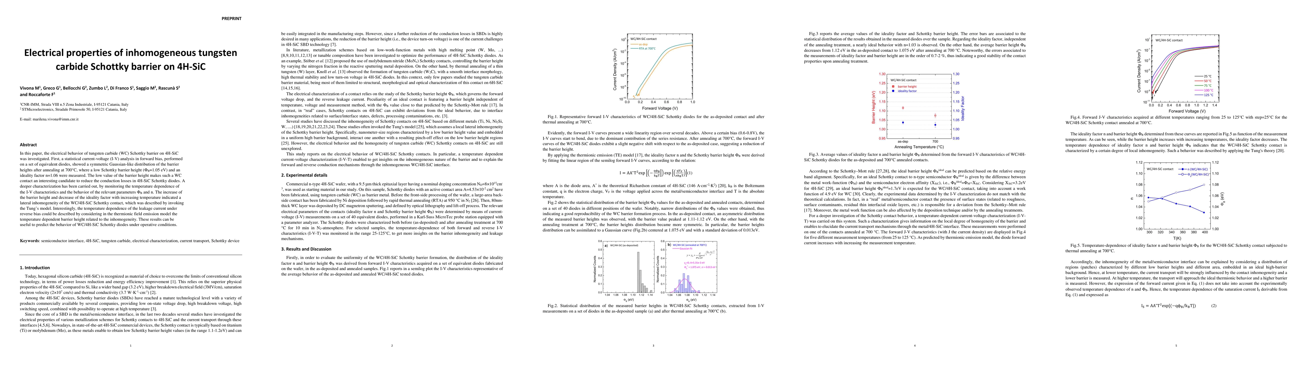
In this paper, the electrical behavior of tungsten carbide (WC) Schottky barrier on 4H-SiC was investigated. First, a statistical current-voltage (I-V) analysis in forward bias, performed on a set o...

Thumbnail for Identification of two trapping mechanisms responsible of the threshold
  voltage variation in SiO$_2$/4H-SiC MOSFETs

Identification of two trapping mechanisms responsible of the threshold voltage variation in SiO$_2$/4H-SiC MOSFETs

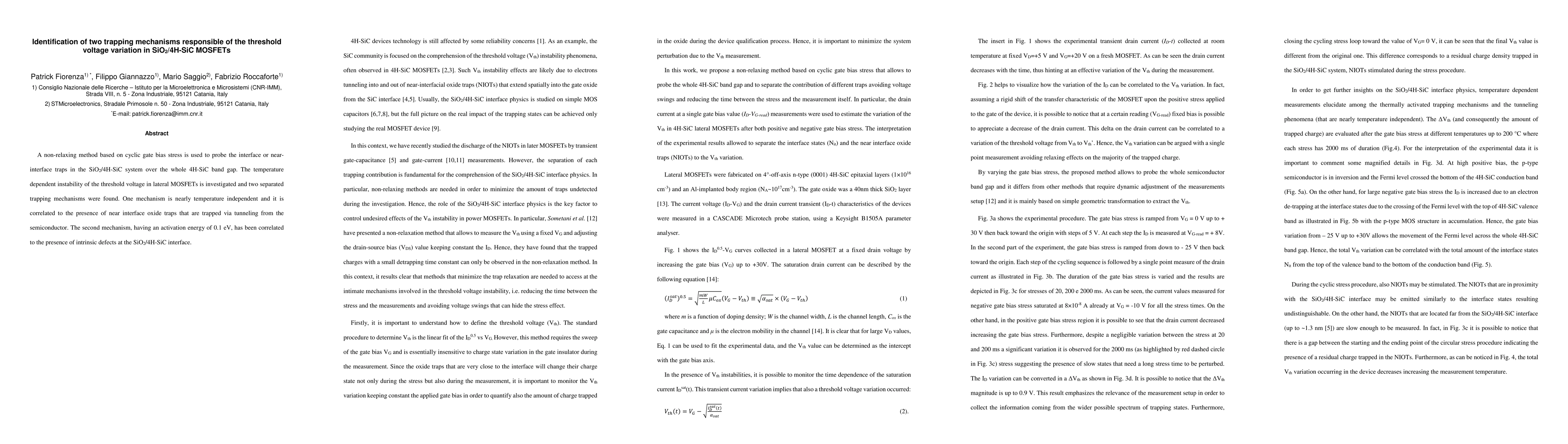
A non-relaxing method based on cyclic gate bias stress is used to probe the interface or near-interface traps in the SiO$_2$/4H-SiC system over the whole 4H-SiC band gap. The temperature dependent i...

Thumbnail for Processing issues in SiC and GaN power devices technology: the cases of
  4H-SiC planar MOSFET and recessed hybrid GaN MISHEMT

Processing issues in SiC and GaN power devices technology: the cases of 4H-SiC planar MOSFET and recessed hybrid GaN MISHEMT

This paper aims to give a short overview on some relevant processing issues existing in SiC and GaN power devices technology. The main focus is put on the importance of the channel mobility in trans...

Thumbnail for Nanolaminated Al2O3/HfO2 dielectrics for silicon carbide based devices

Nanolaminated Al2O3/HfO2 dielectrics for silicon carbide based devices

Nanolaminated Al2O3/HfO2 thin films as well as single Al2O3 and HfO2 layers have been grown as gate dielectrics by Plasma Enhanced Atomic Layer Deposition (PEALD) technique on silicon carbide (4H-Si...

Thumbnail for Electron trapping at SiO2/4H-SiC interface probed by transient
  capacitance measurements and atomic resolution chemical analysis

Electron trapping at SiO2/4H-SiC interface probed by transient capacitance measurements and atomic resolution chemical analysis

Studying the electrical and structural properties of the interface of the gate oxide (SiO2) with silicon carbide (4H-SiC) is a fundamental topic, with important implications for understanding and op...

Thumbnail for Impact of the NO annealing duration on the SiO2/4H-SiC interface
  properties in lateral MOSFETs: the energetic profile of the
  near-interface-oxide traps

Impact of the NO annealing duration on the SiO2/4H-SiC interface properties in lateral MOSFETs: the energetic profile of the near-interface-oxide traps

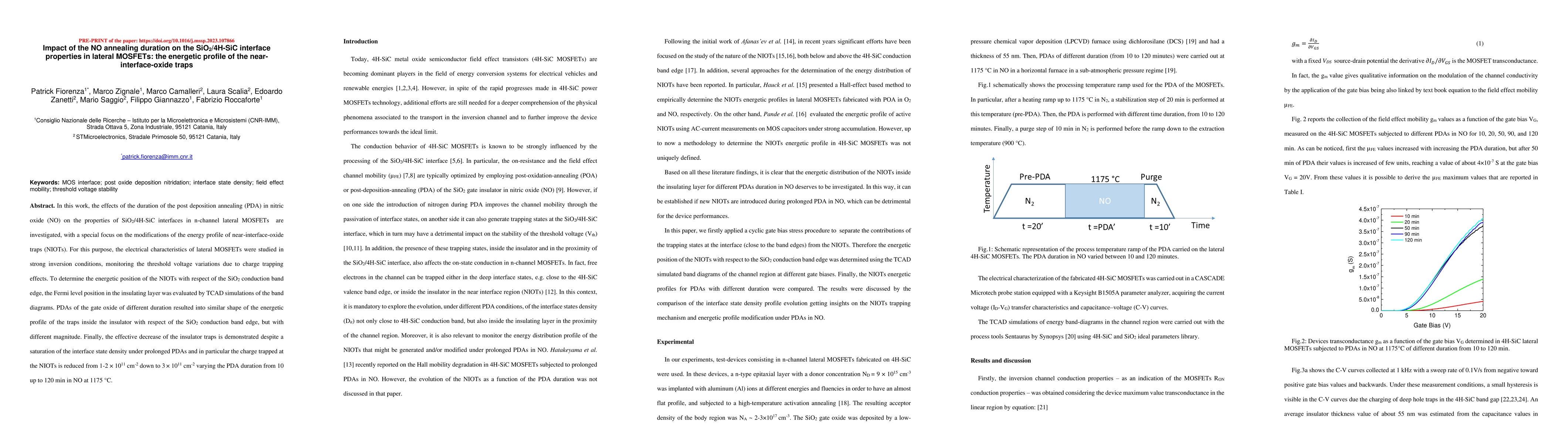
In this work, the effects of the duration of the post deposition annealing (PDA) in nitric oxide (NO) on the properties of SiO2/4H-SiC interfaces in n-channel lateral MOSFETs are investigated, with a ...

Thumbnail for Complementary two dimensional carrier profiles of 4H-SiC MOSFETs by
  Scanning Spreading Resistance Microscopy and Scanning Capacitance Microscopy

Complementary two dimensional carrier profiles of 4H-SiC MOSFETs by Scanning Spreading Resistance Microscopy and Scanning Capacitance Microscopy

This paper reports the results presented in an invited poster during the International Conference on Silicon Carbide and Related Materials (ICSCRM) 2023 held in Sorrento, Italy. The suitability of sca...

This website uses cookies to ensure you get the best experience. Learn more