ArxivLens
F
Researcher

Fengwen Mu

6 papers on arXiv

6 arXiv Papers
79 Total Publications
Profile

Academic Profile

Name F. Mu
Total Papers 79
Scholar Profile View on Semantic Scholar
Metrics

Statistics

6 arXiv Papers
79 Total Publications
Publications

Papers on arXiv

Thumbnail for Enhancing and Mapping Thermal Boundary Conductance across Bonded Si/SiC
  Interface
arXiv
Enhancing and Mapping Thermal Boundary Conductance across Bonded Si/SiC Interface

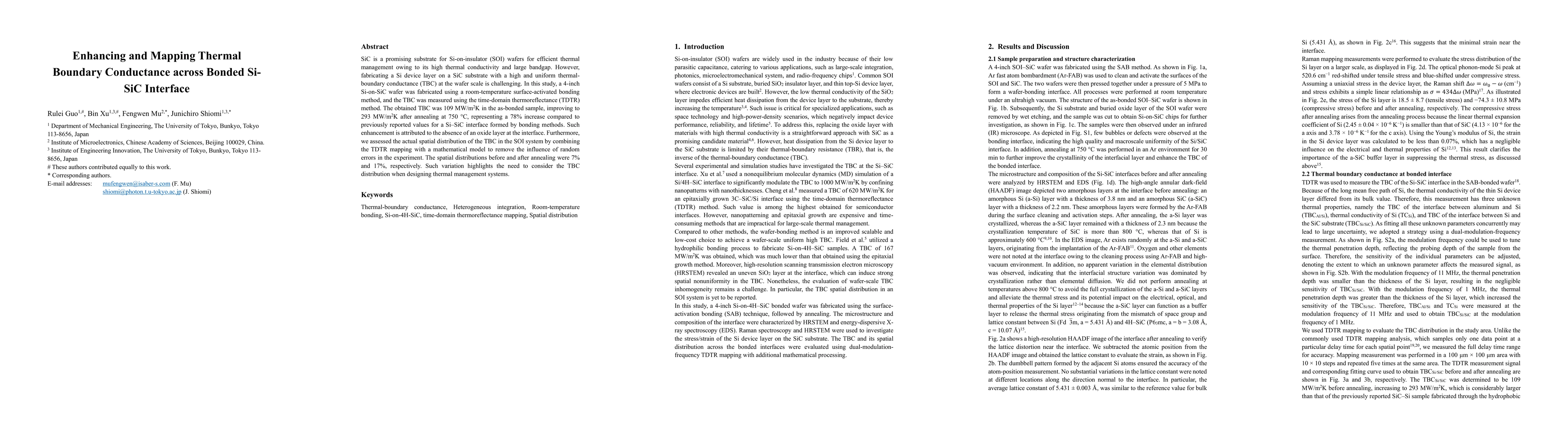
SiC is a promising substrate for Si-on-insulator (SOI) wafers for efficient thermal management owing to its high thermal conductivity and large bandgap. However, fabricating a Si device layer on a S...

Thumbnail for Low thermal boundary resistance at bonded GaN/diamond interface by
  controlling ultrathin heterogeneous amorphous layer
arXiv
Low thermal boundary resistance at bonded GaN/diamond interface by controlling ultrathin heterogeneous amorphous layer

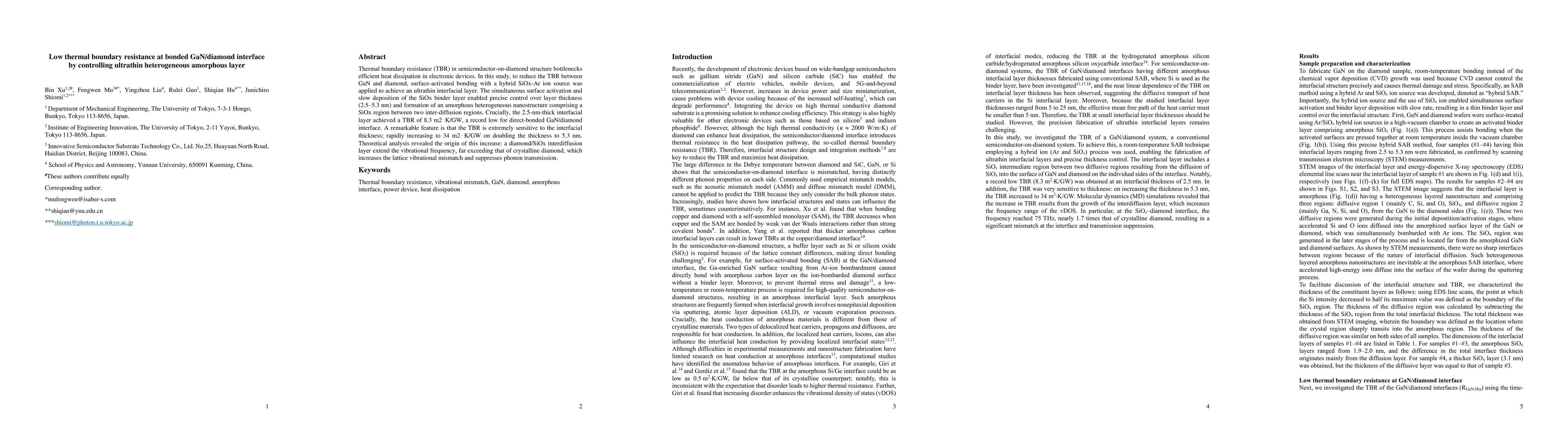
Thermal boundary resistance (TBR) in semiconductor-on-diamond structure bottlenecks efficient heat dissipation in electronic devices. In this study, to reduce the TBR between GaN and diamond, surfac...

Thumbnail for A Novel Strategy for GaN-on-Diamond Device with a High Thermal Boundary
  Conductance
arXiv
A Novel Strategy for GaN-on-Diamond Device with a High Thermal Boundary Conductance

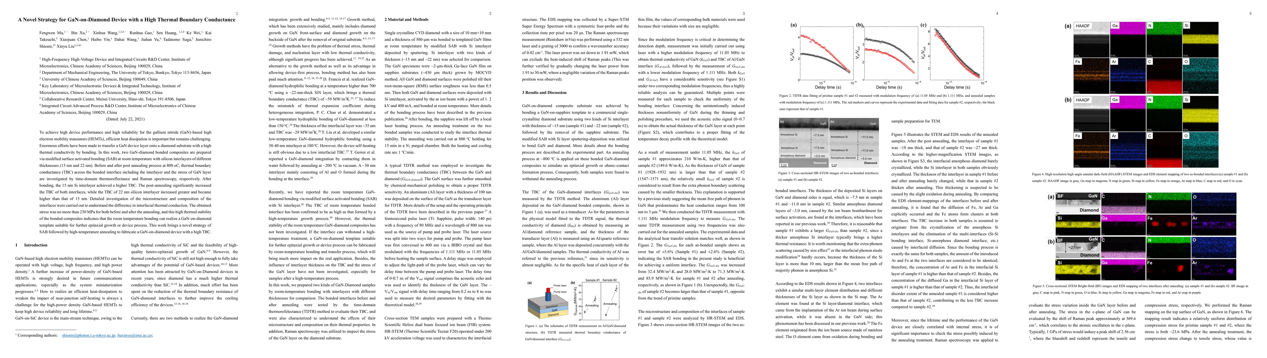
To achieve high device performance and high reliability for the gallium nitride (GaN)-based high electron mobility transistors (HEMTs), efficient heat dissipation is important but remains challengin...

Thumbnail for Thermal Visualization of Buried Interfaces by Transient and Steady-State
  Responses of Time-Domain Thermoreflectance
arXiv
Thermal Visualization of Buried Interfaces by Transient and Steady-State Responses of Time-Domain Thermoreflectance

Thermal resistances from interfaces impede heat dissipation in micro/nanoscale electronics, especially for high-power electronics. Despite the growing importance of understanding interfacial thermal...

Thumbnail for Wafer-scale Heterogeneous Integration of Monocrystalline \b{eta}-Ga2O3
  Thin Films on SiC for Thermal Management by Ion-Cutting Technique
arXiv
Wafer-scale Heterogeneous Integration of Monocrystalline \b{eta}-Ga2O3 Thin Films on SiC for Thermal Management by Ion-Cutting Technique

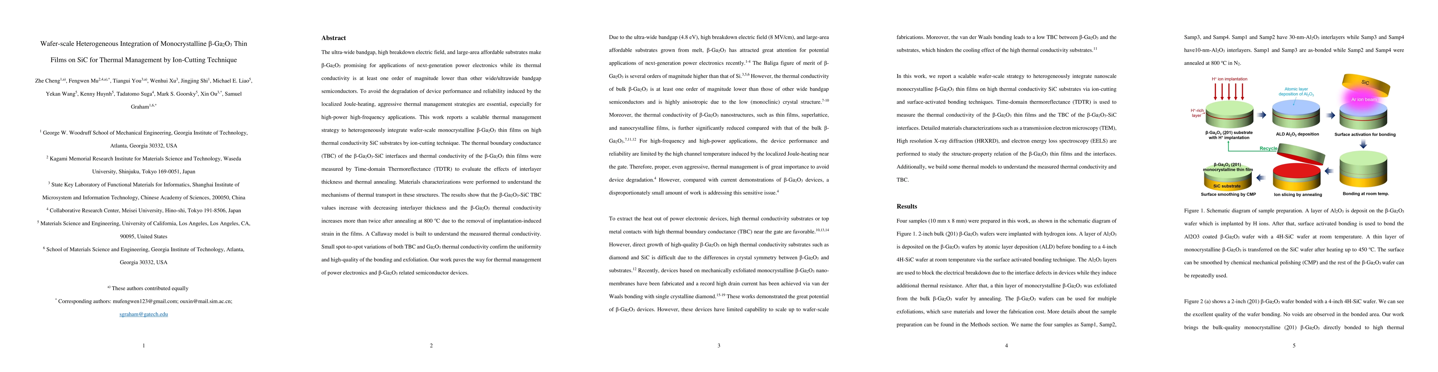
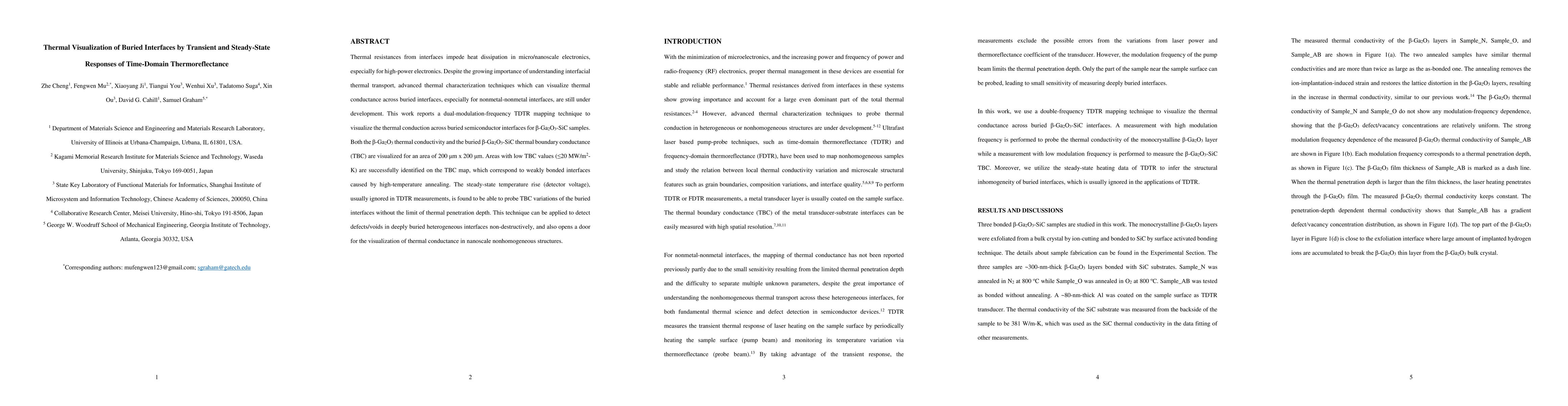
The ultra-wide bandgap, high breakdown electric field, and large-area affordable substrates make \b{eta}-Ga2O3 promising for applications of next-generation power electronics while its thermal condu...

Thumbnail for Interfacial Thermal Conductance across Room-Temperature Bonded
  GaN-Diamond Interfaces for GaN-on-Diamond Devices
arXiv
Interfacial Thermal Conductance across Room-Temperature Bonded GaN-Diamond Interfaces for GaN-on-Diamond Devices

The wide bandgap, high-breakdown electric field, and high carrier mobility makes GaN an ideal material for high-power and high-frequency electronics applications such as wireless communication and r...

This website uses cookies to ensure you get the best experience. Learn more