Academic Profile
Statistics
Similar Authors
Papers on arXiv
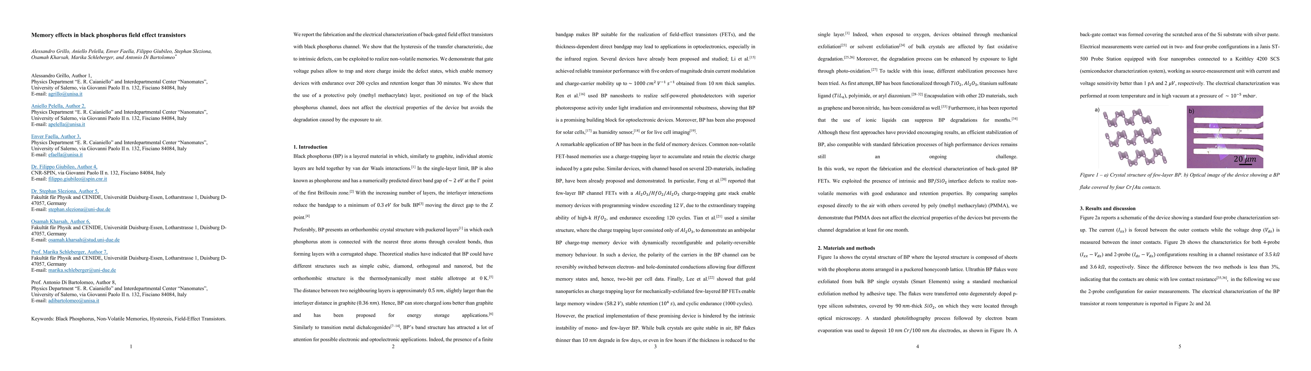
We report the fabrication and the electrical characterization of back-gated field effect transistors with black phosphorus channel. We show that the hysteresis of the transfer characteristic, due to...
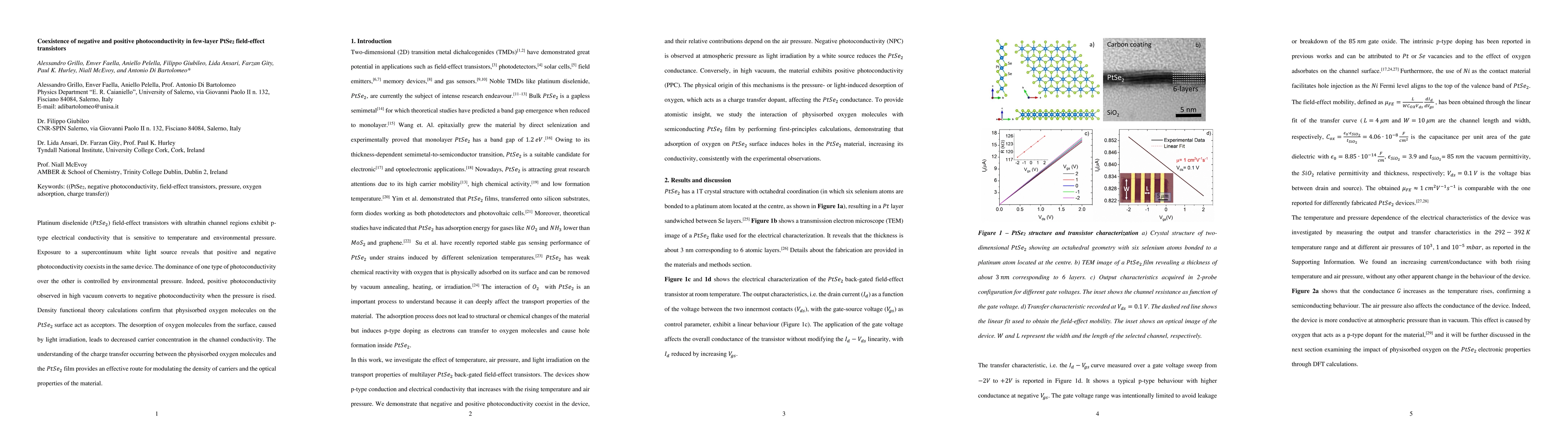
Platinum diselenide (PtSe_2) field-effect transistors with ultrathin channel regions exhibit p-type electrical conductivity that is sensitive to temperature and environmental pressure. Exposure to a...
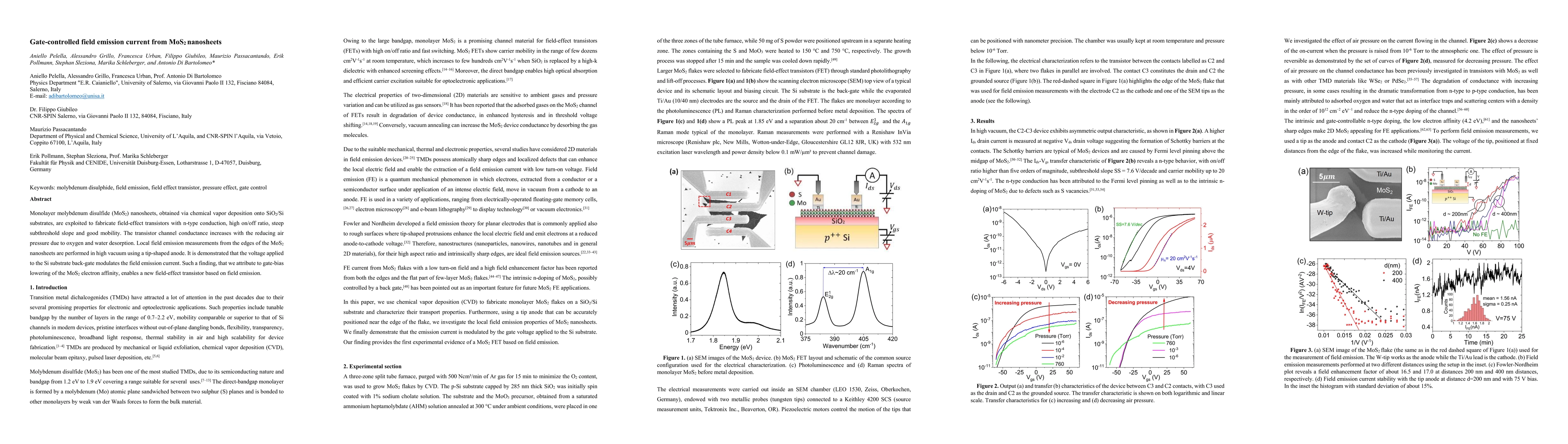
Monolayer molybdenum disulfide (MoS$_2$) nanosheets, obtained via chemical vapor deposition onto SiO$_2$/Si substrates, are exploited to fabricate field-effect transistors with n-type conduction, hi...
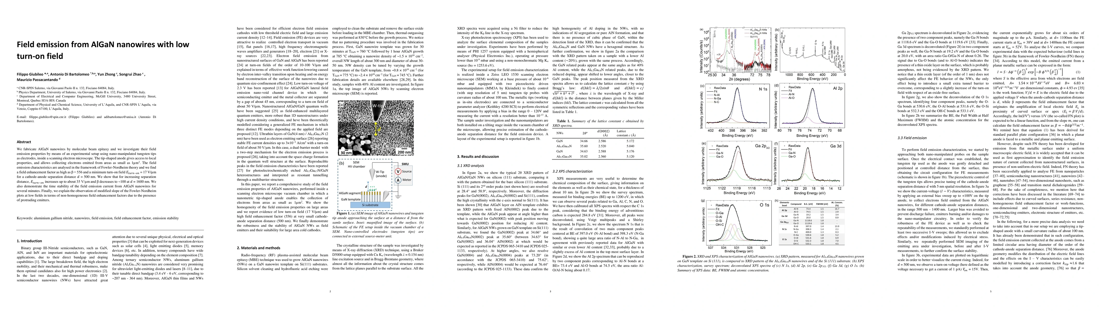
We fabricate AlGaN nanowires by molecular beam epitaxy and we investigate their field emission properties by means of an experimental setup using nano-manipulated tungsten tips as electrodes, inside...
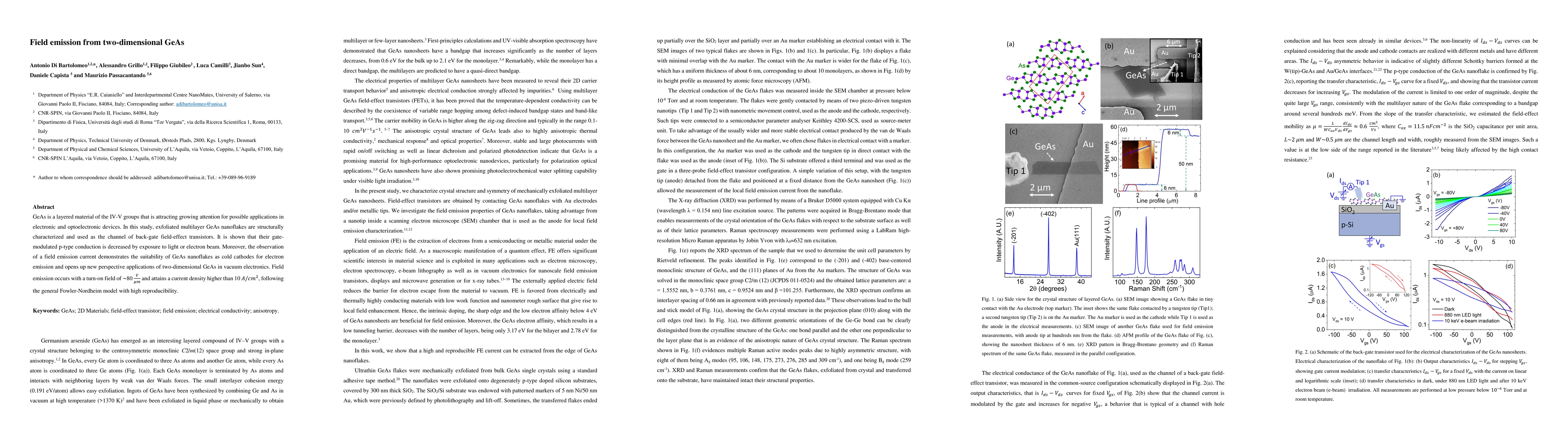
GeAs is a layered material of the IV-V groups that is attracting growing attention for possible applications in electronic and optoelectronic devices. In this study, exfoliated multilayer GeAs nanof...
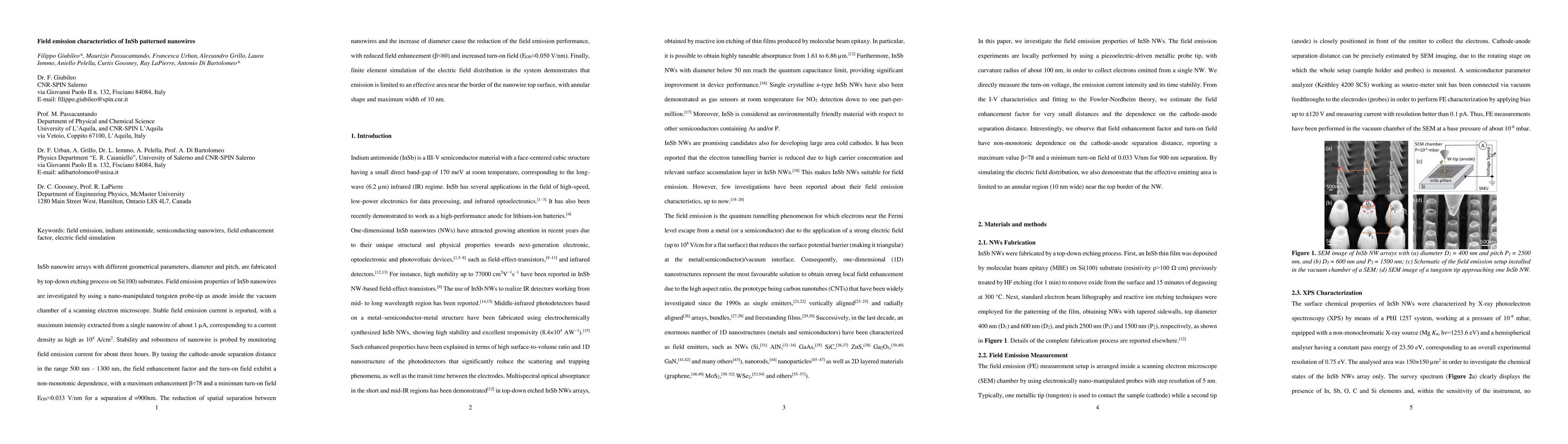
InSb nanowire arrays with different geometrical parameters, diameter and pitch, are fabricated by top-down etching process on Si(100) substrates. Field emission properties of InSb nanowires are inve...
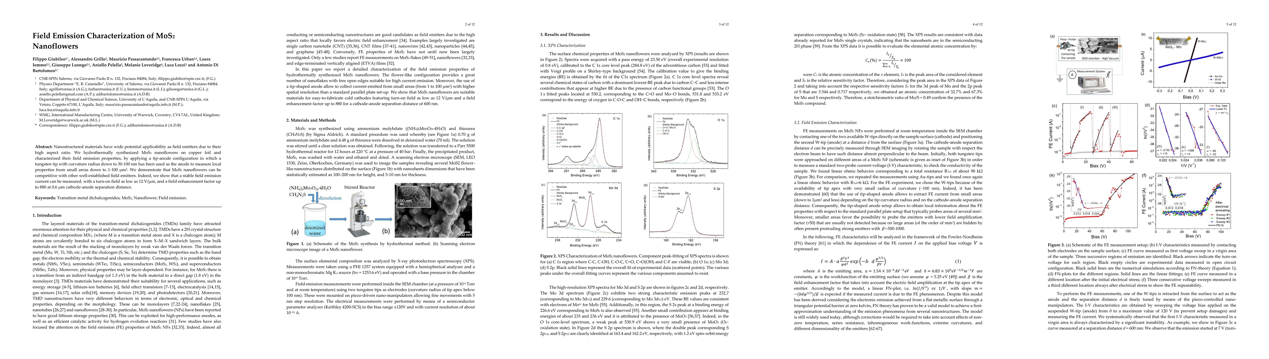
Nanostructured materials have wide potential applicability as field emitters due to their high aspect ratio. We hydrothermally synthesized MoS2 nanoflowers on copper foil and characterized their fie...
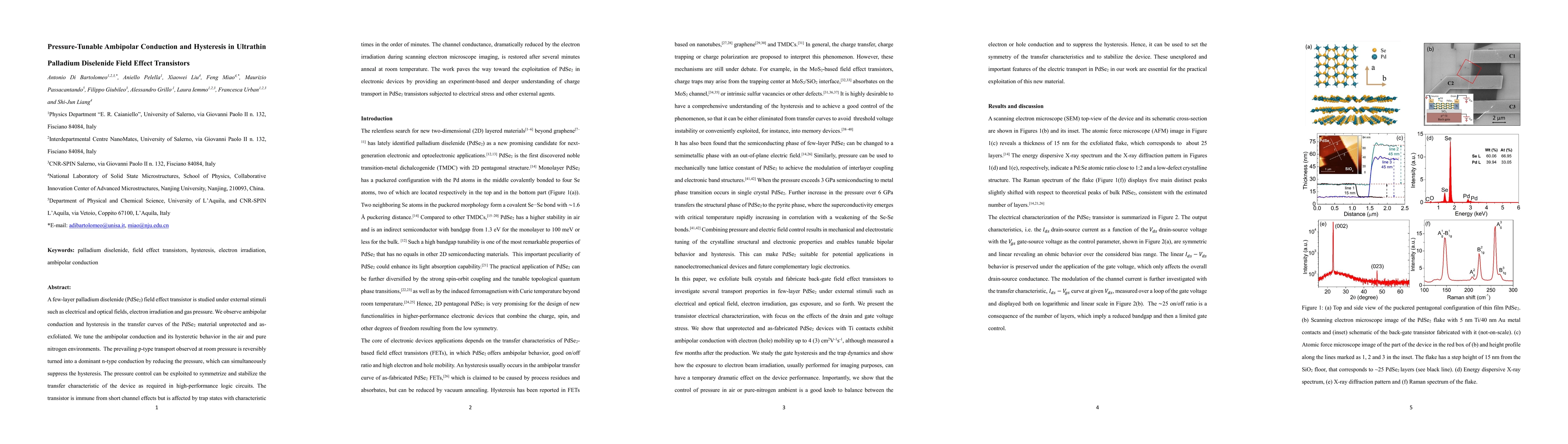
A few-layer palladium diselenide (PdSe2) field effect transistor is studied under external stimuli such as electrical and optical fields, electron irradiation and gas pressure. We observe ambipolar ...