Academic Profile
Statistics
Similar Authors
Papers on arXiv
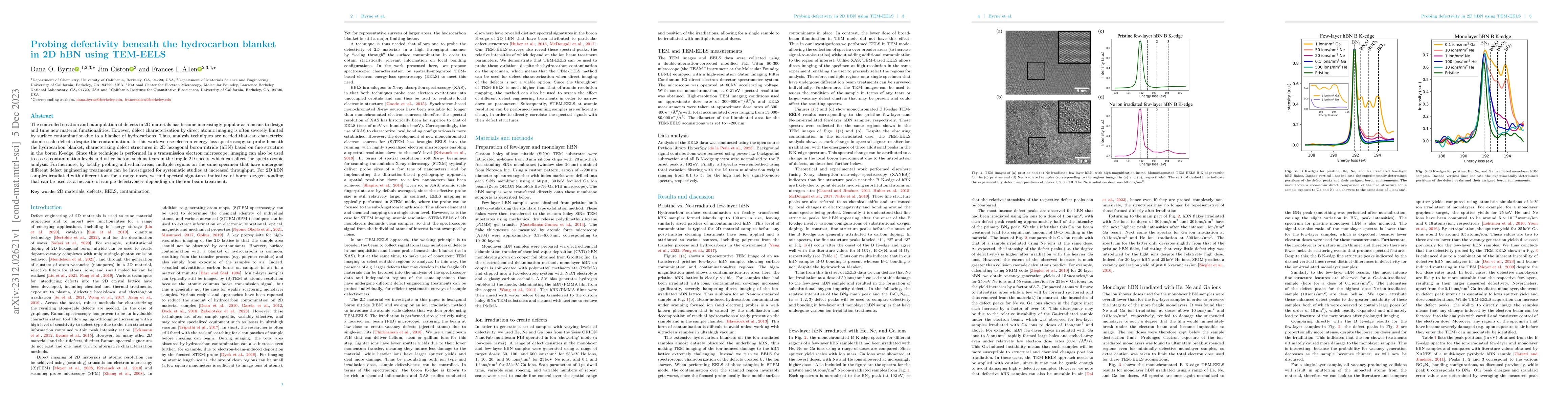
The controlled creation and manipulation of defects in 2D materials has become increasingly popular as a means to design and tune new material functionalities. However, defect characterization by di...

We demonstrate the fabrication of sharp nanopillars of high aspect ratio onto specialized atomic force microscopy (AFM) microcantilevers and their use for high-speed AFM of DNA and nucleoproteins in...
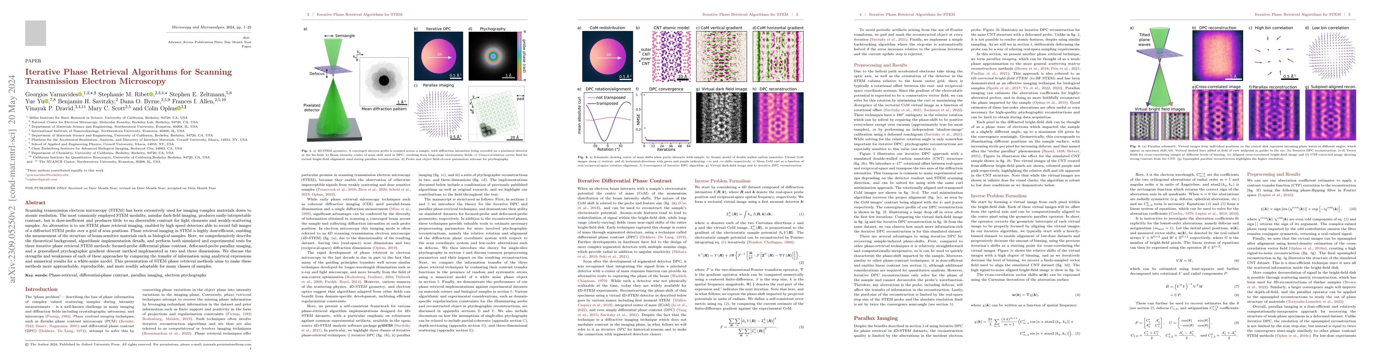
Scanning transmission electron microscopy (STEM) has been extensively used for imaging complex materials down to atomic resolution. The most commonly employed STEM modality, annular dark-field imagi...
The focused ion beam (FIB) is a powerful tool for the fabrication, modification and characterization of materials down to the nanoscale. Starting with the gallium FIB, which was originally intended ...
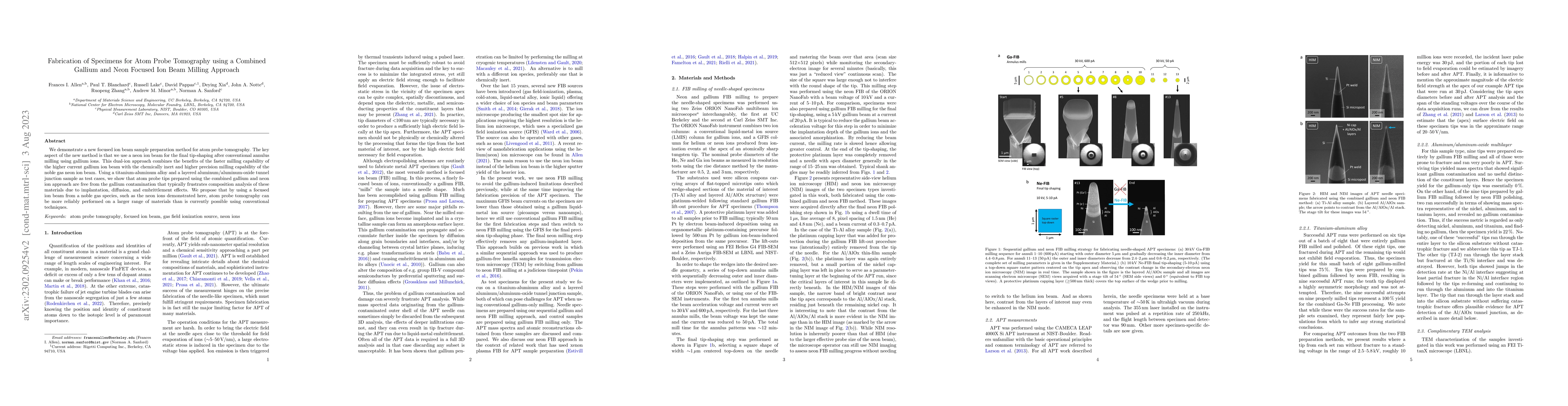
We demonstrate a new focused ion beam sample preparation method for atom probe tomography. The key aspect of the new method is that we use a neon ion beam for the final tip-shaping after conventiona...
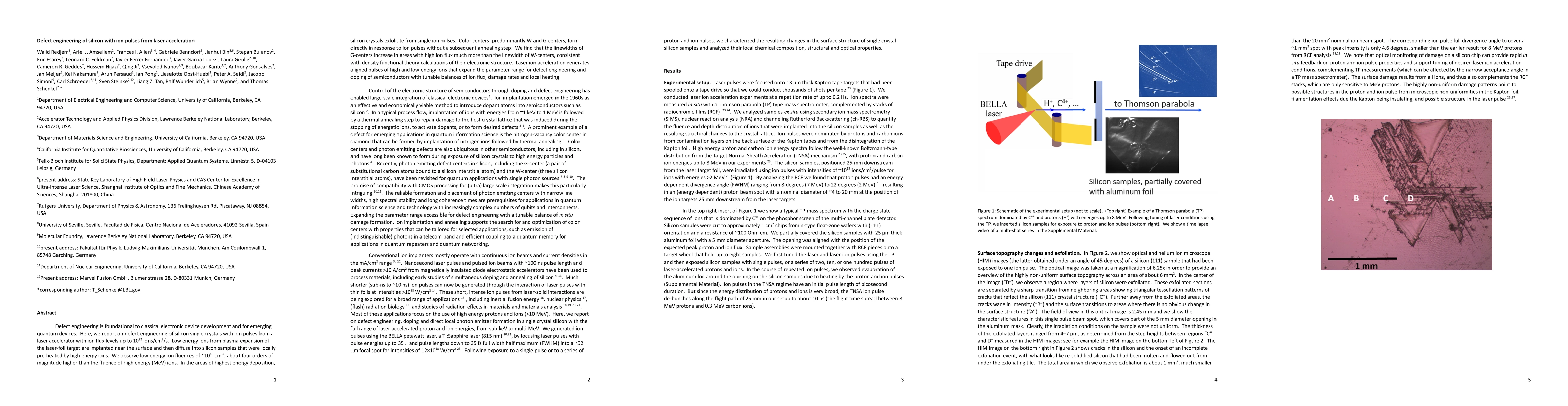
Defect engineering is foundational to classical electronic device development and for emerging quantum devices. Here, we report on defect engineering of silicon single crystals with ion pulses from ...
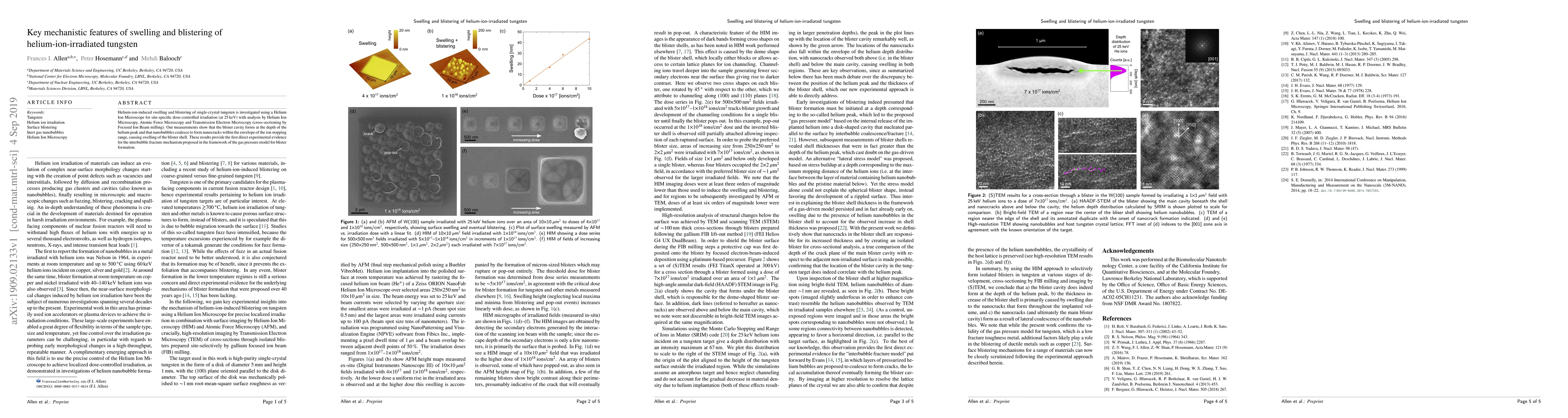
Helium-ion-induced swelling and blistering of single-crystal tungsten is investigated using a Helium Ion Microscope for site-specific dose-controlled irradiation (at 25 keV) with analysis by Helium ...
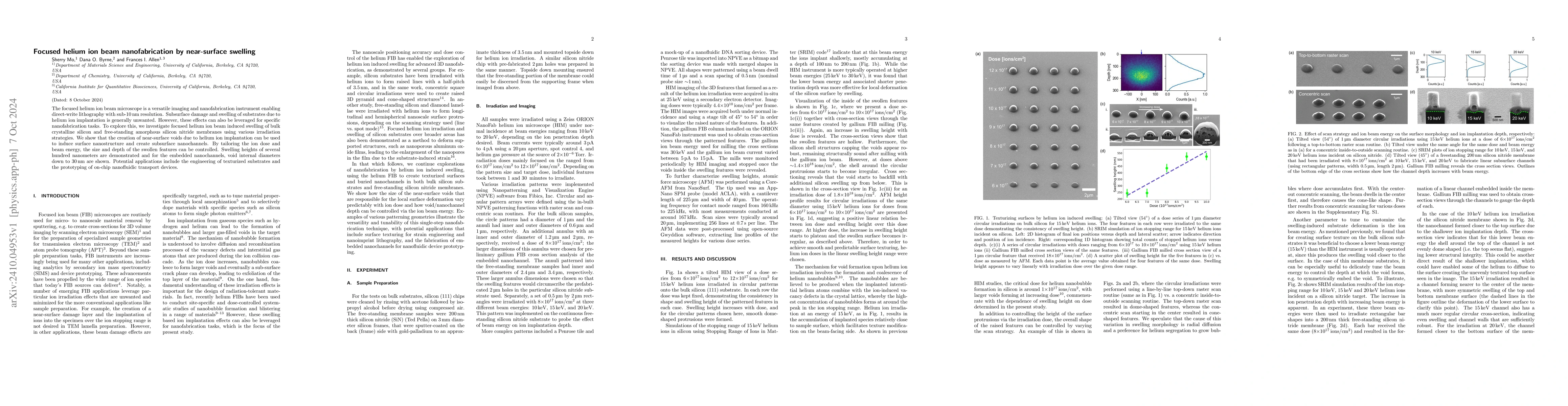
The focused helium ion beam microscope is a versatile imaging and nanofabrication instrument enabling direct-write lithography with sub-10-nm resolution. Subsurface damage and swelling of substrates d...
Nanopores in 2D materials are of significant interest in advanced membrane technologies aimed at the sensing and separation of ions and molecules. These applications necessitate 2D nanopores that are ...
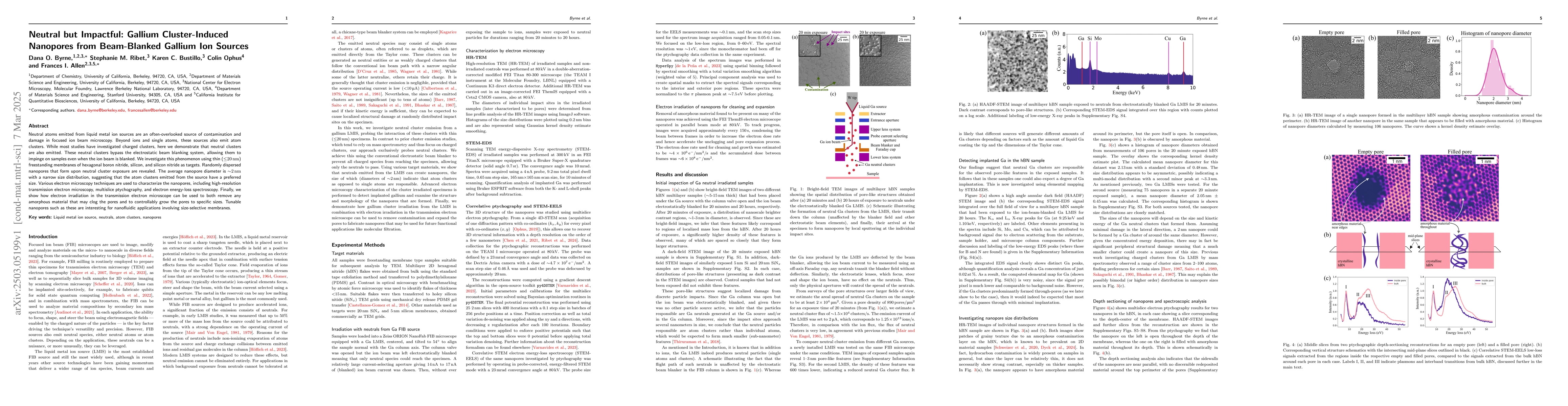
Neutral atoms emitted from liquid metal ion sources are an often-overlooked source of contamination and damage in focused ion beam microscopy. Beyond ions and single atoms, these sources also emit ato...
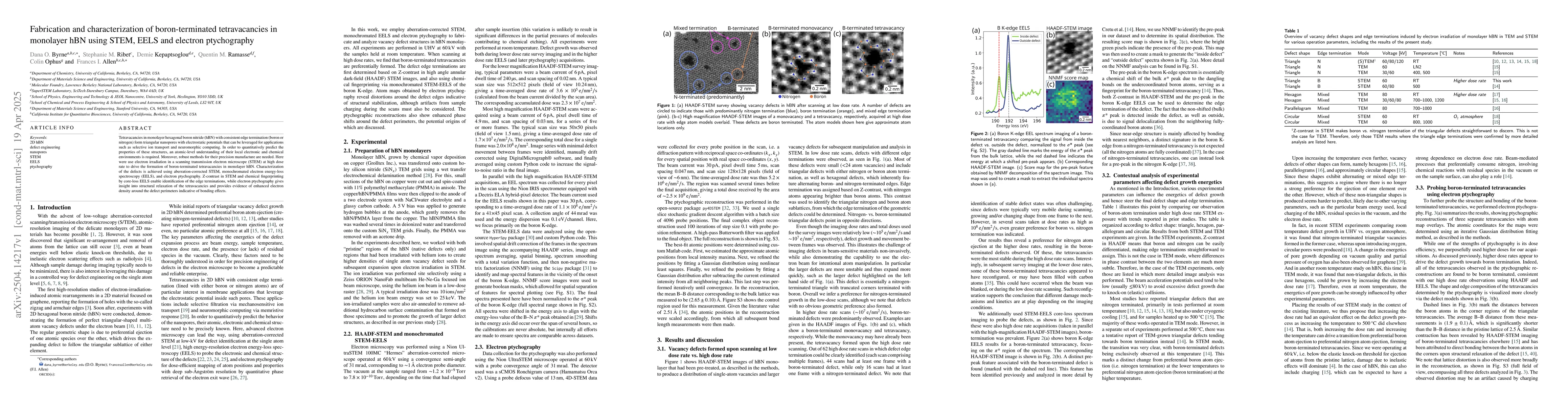
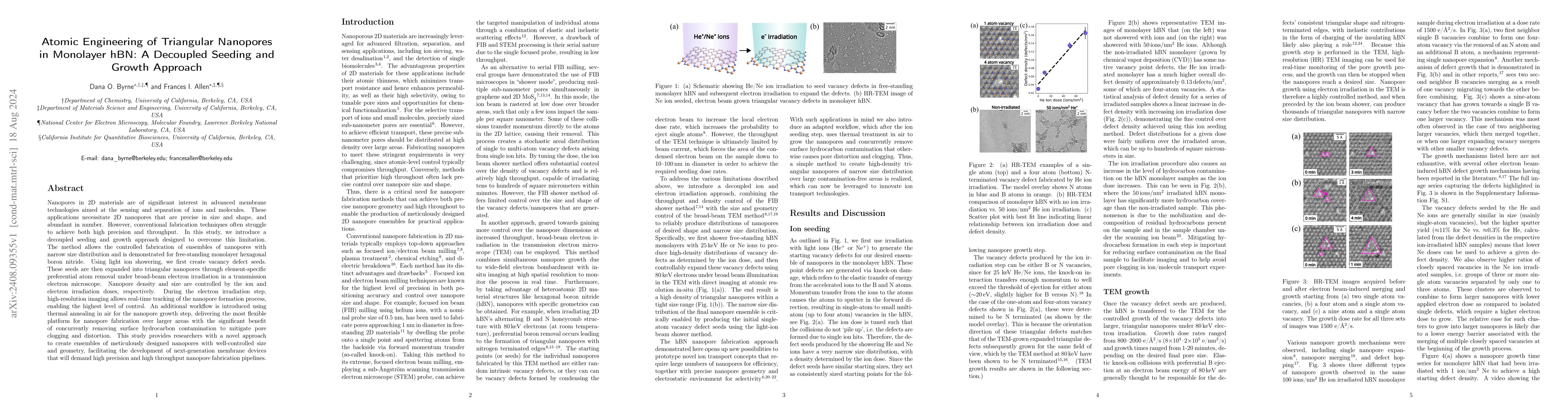
Tetravacancies in monolayer hexagonal boron nitride (hBN) with consistent edge termination (boron or nitrogen) form triangular nanopores with electrostatic potentials that can be leveraged for applica...