Academic Profile
Statistics
Similar Authors
Papers on arXiv
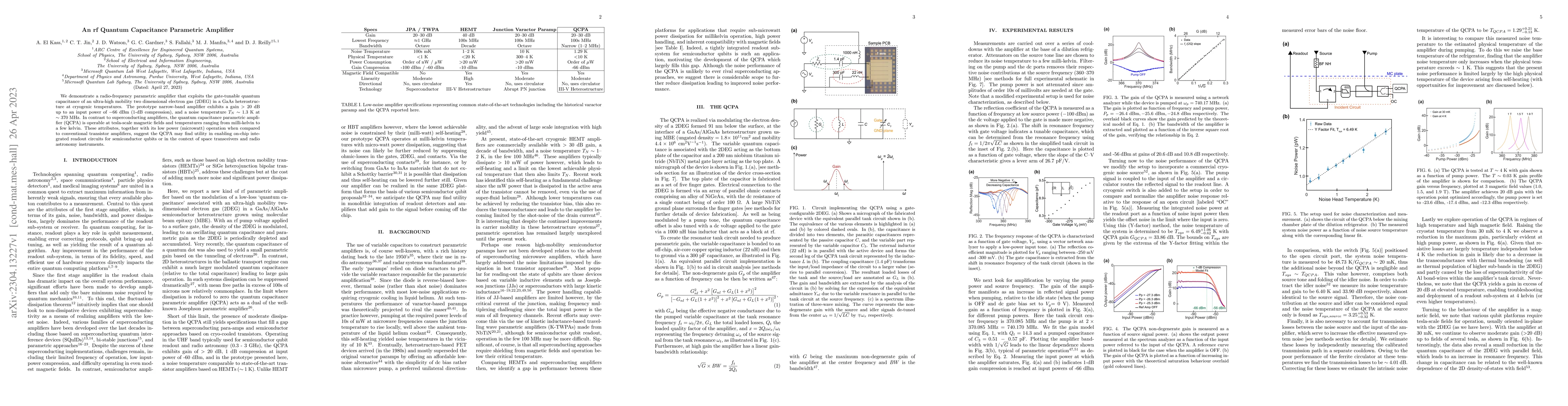
We demonstrate a radio-frequency parametric amplifier that exploits the gate-tunable quantum capacitance of an ultra high mobility two dimensional electron gas (2DEG) in a GaAs heterostructure at cr...
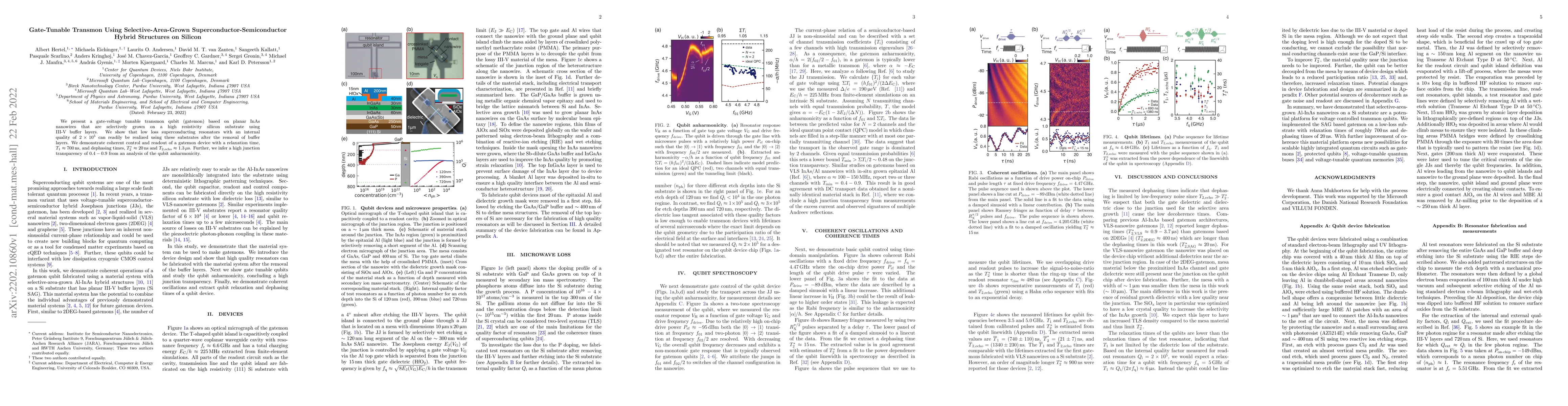
We present a gate-voltage tunable transmon qubit (gatemon) based on planar InAs nanowires that are selectively grown on a high resistivity silicon substrate using III-V buffer layers. We show that l...
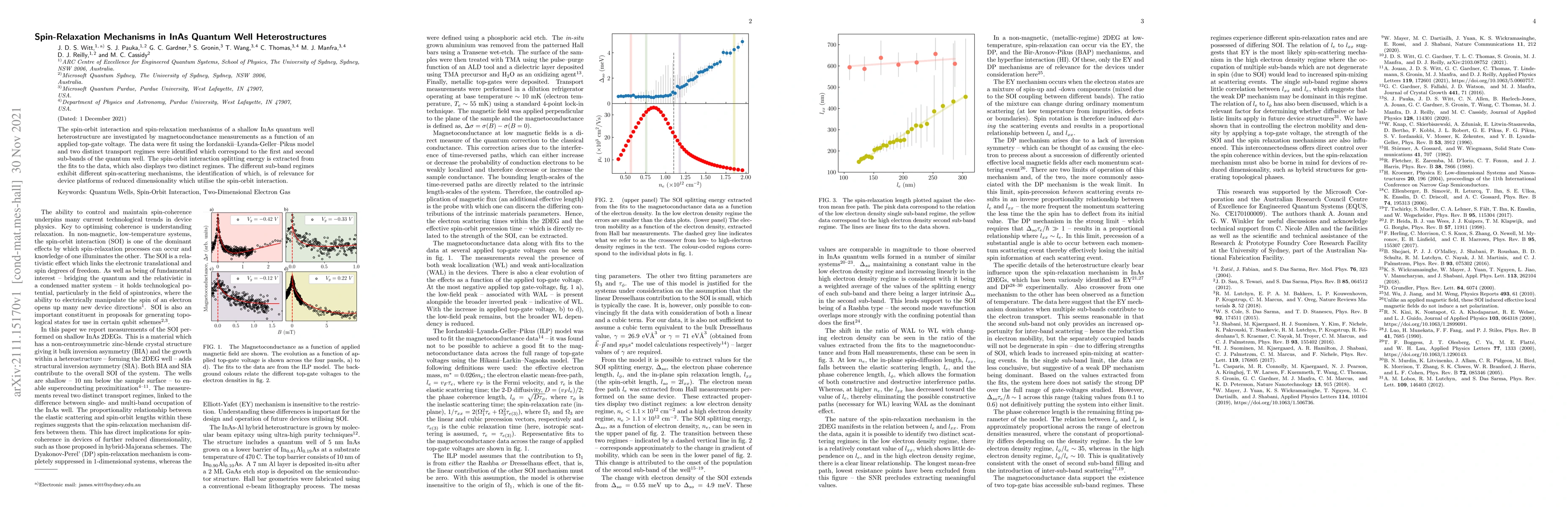
The spin-orbit interaction and spin-relaxation mechanisms of a shallow InAs quantum well heterostructure are investigated by magnetoconductance measurements as a function of an applied top-gate volt...
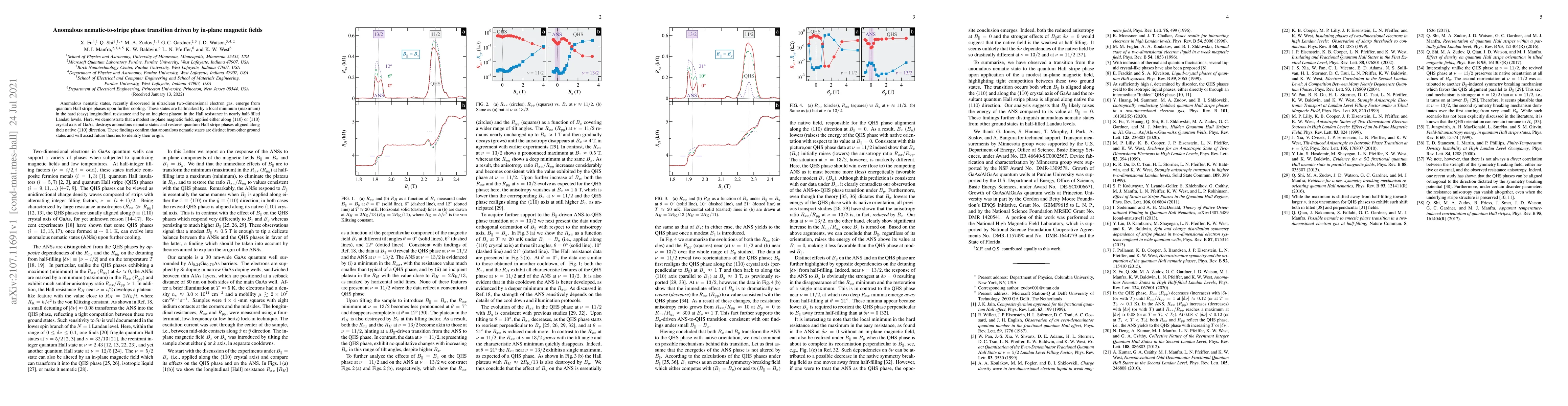
Anomalous nematic states, recently discovered in ultraclean two-dimensional electron gas, emerge from quantum Hall stripe phases upon further cooling. These states are hallmarked by a local minimum ...
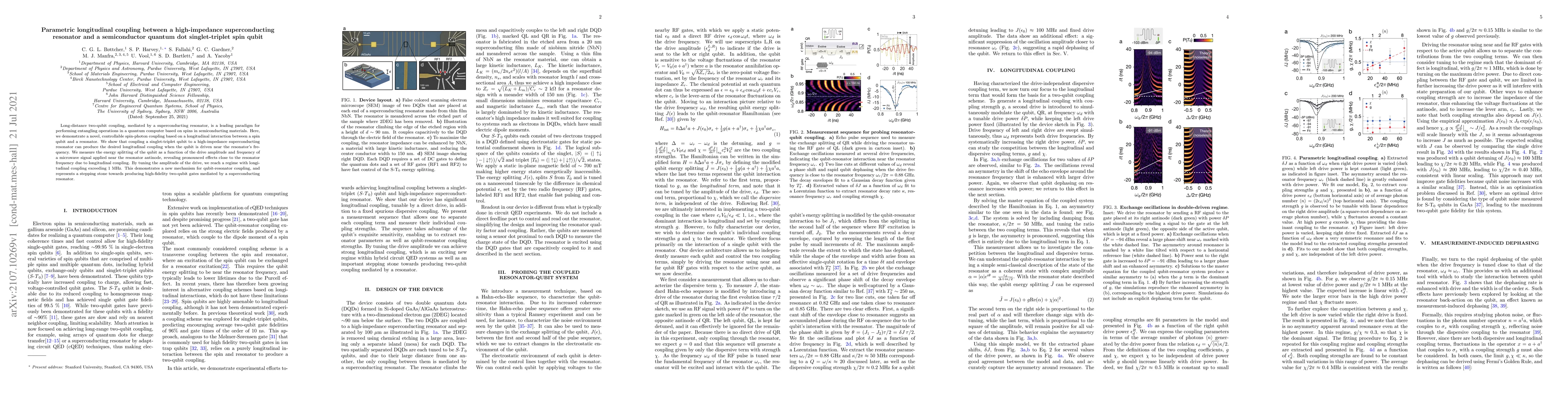
Long-distance two-qubit coupling, mediated by a superconducting resonator, is a leading paradigm for performing entangling operations in a quantum computer based on spins in semiconducting materials...
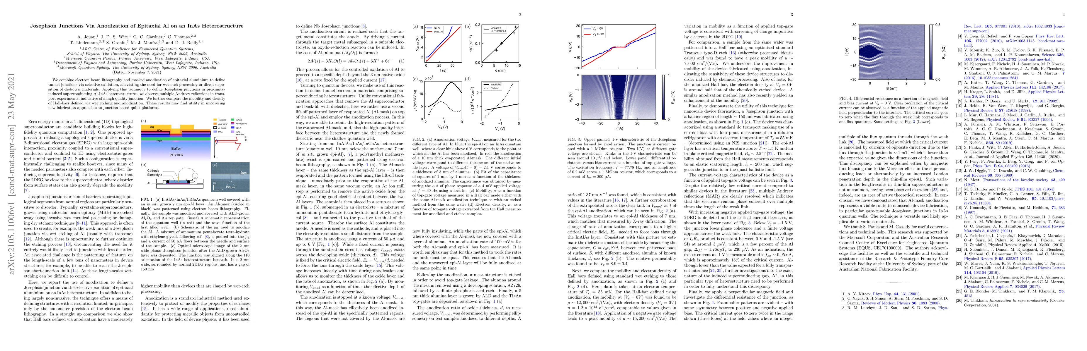
We combine electron beam lithography and masked anodization of epitaxial aluminium to define tunnel junctions via selective oxidation, alleviating the need for wet-etch processing or direct depositi...
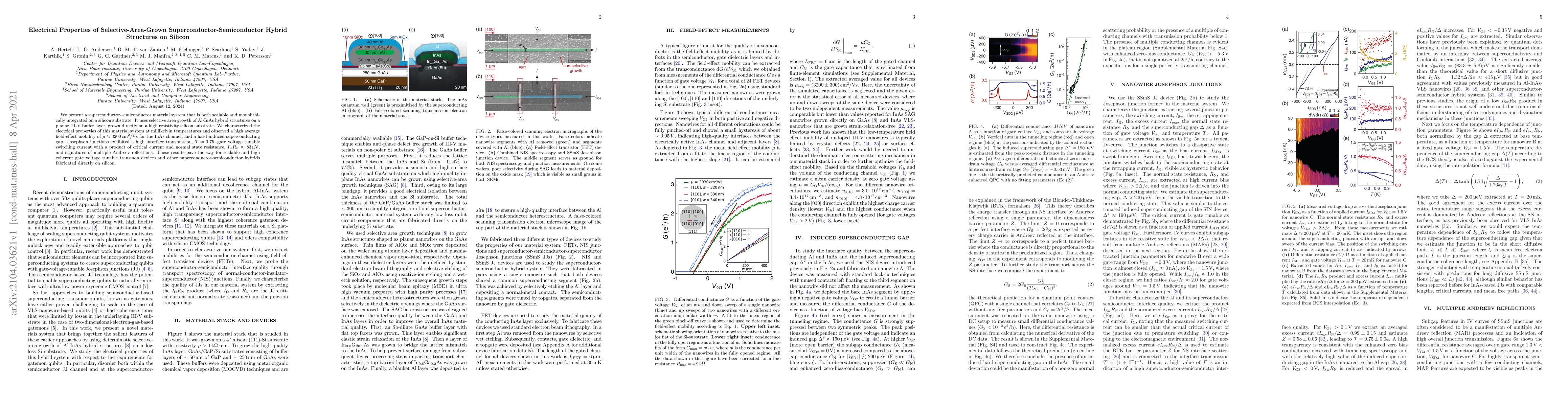
We present a superconductor-semiconductor material system that is both scalable and monolithically integrated on a silicon substrate. It uses selective area growth of Al-InAs hybrid structures on a ...
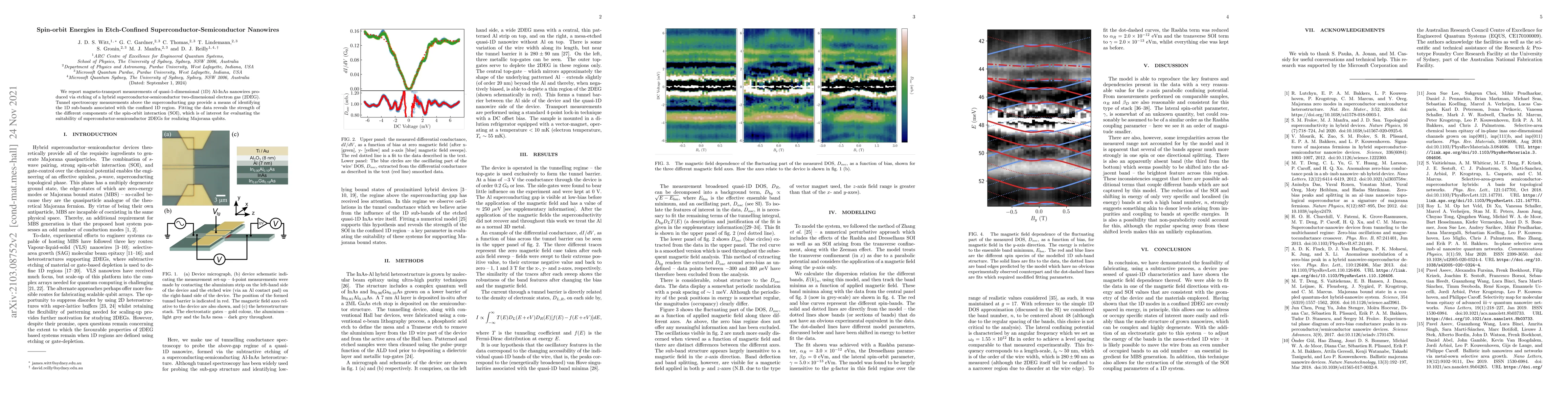
We report magneto-transport measurements of quasi-1-dimensional (1D) Al-InAs nanowires produced via etching of a hybrid superconductor-semiconductor two-dimensional electron gas (2DEG). Tunnel spect...
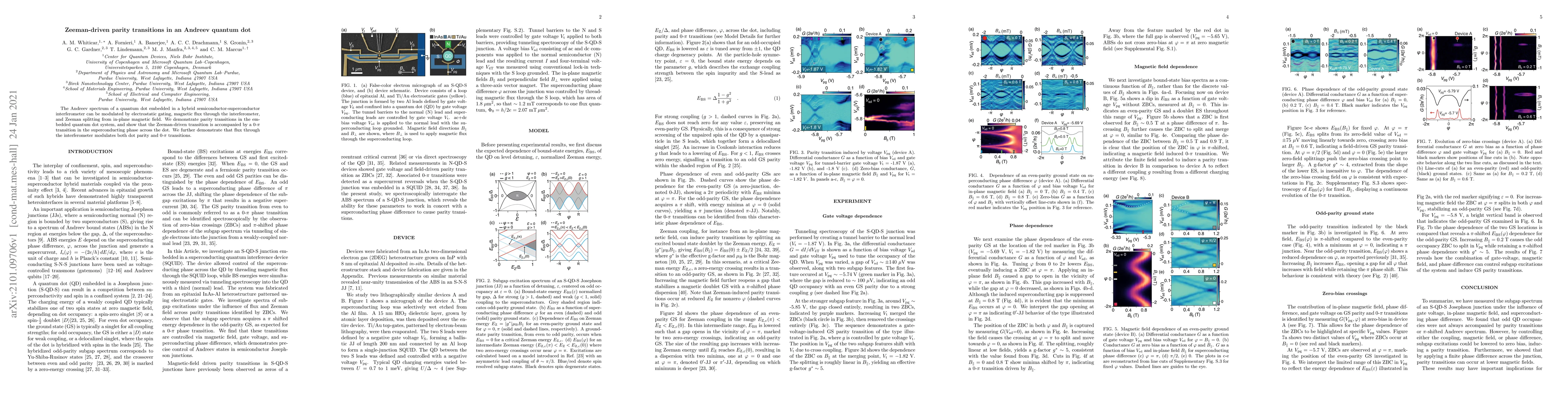
The Andreev spectrum of a quantum dot embedded in a hybrid semiconductor-superconductor interferometer can be modulated by electrostatic gating, magnetic flux through the interferometer, and Zeeman ...
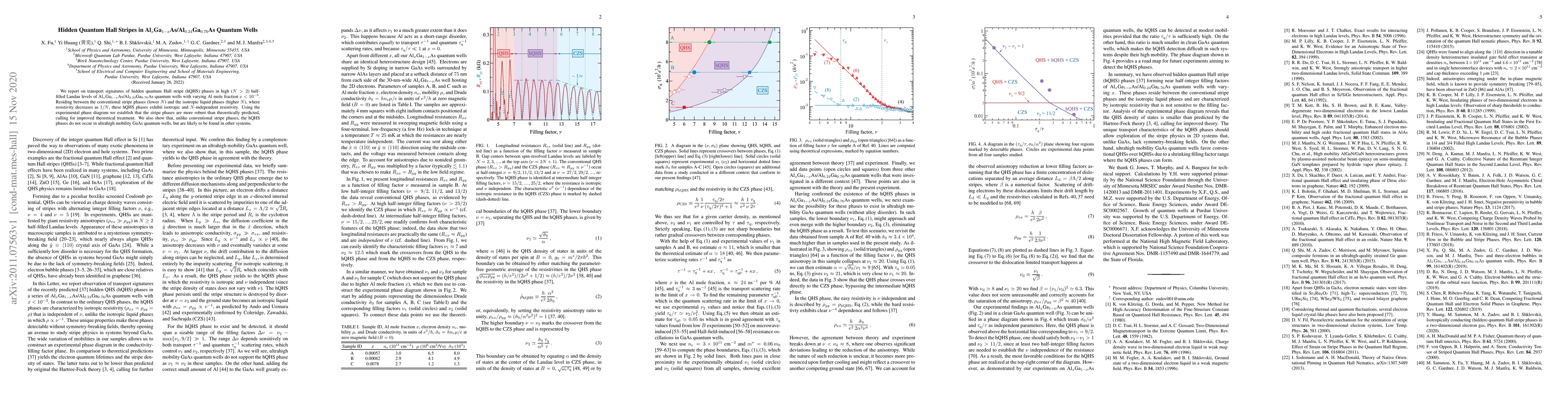
We report on transport signatures of hidden quantum Hall stripe (hQHS) phases in high ($N > 2$) half-filled Landau levels of Al$_{x}$Ga$_{1-x}$As/Al$_{0.24}$Ga$_{0.76}$As quantum wells with varying ...
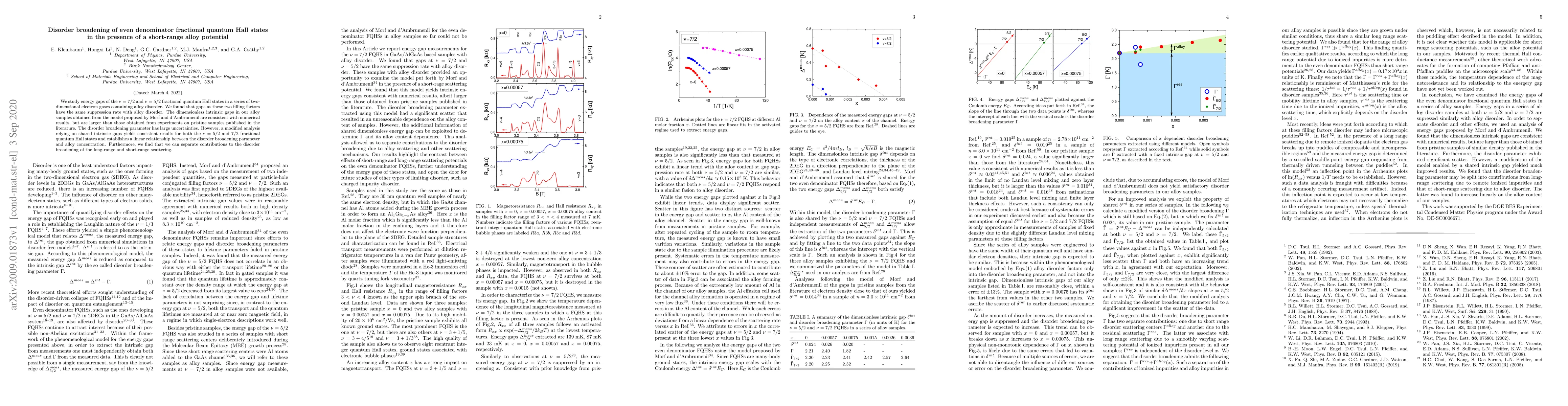
We study energy gaps of the $\nu=7/2$ and $\nu=5/2$ fractional quantum Hall states in a series of two-dimensional electron gases containing alloy disorder. We found that gaps at these two filling fa...
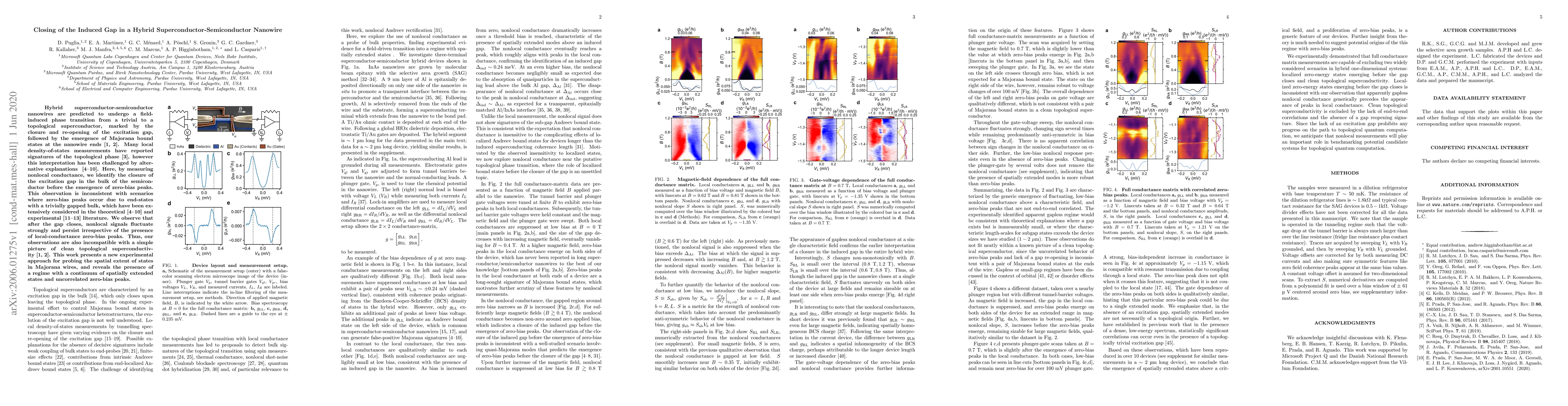
Hybrid superconductor-semiconductor nanowires are predicted to undergo a field-induced phase transition from a trivial to a topological superconductor, marked by the closure and re-opening of the ex...
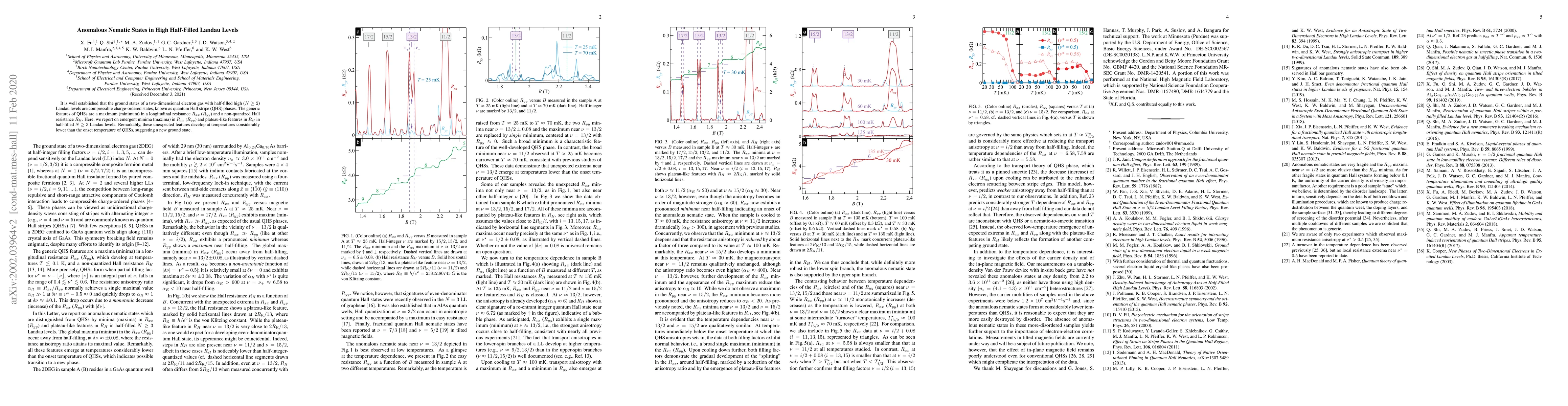
It is well established that the ground states of a two-dimensional electron gas with half-filled high ($N \ge 2$) Landau levels are compressible charge-ordered states, known as quantum Hall stripe (...
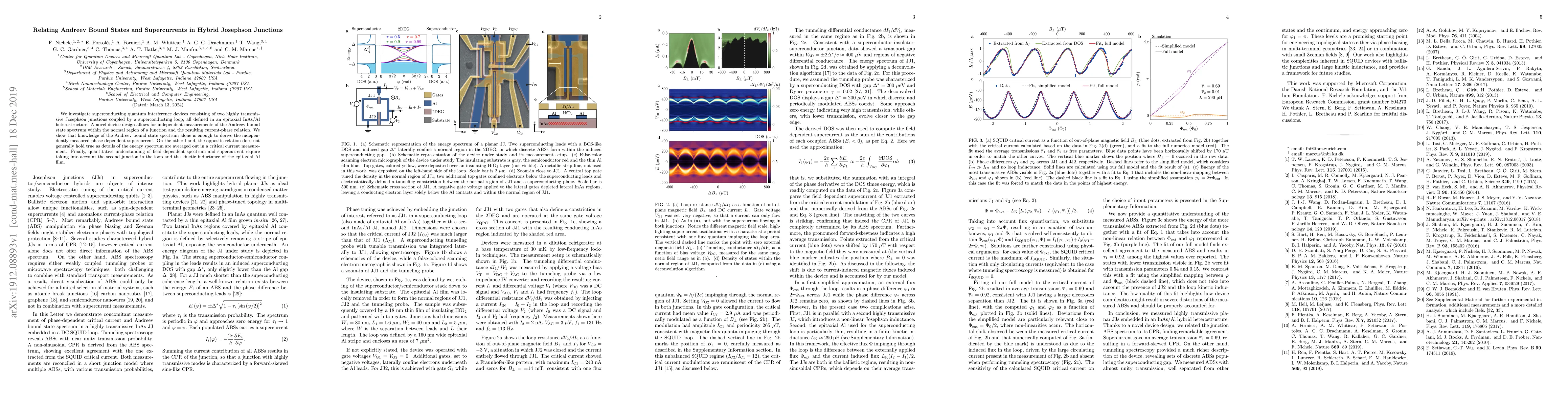
We investigate superconducting quantum interference devices consisting of two highly transmissive Josephson junctions coupled by a superconducting loop, all defined in an epitaxial InAs/Al heterostr...
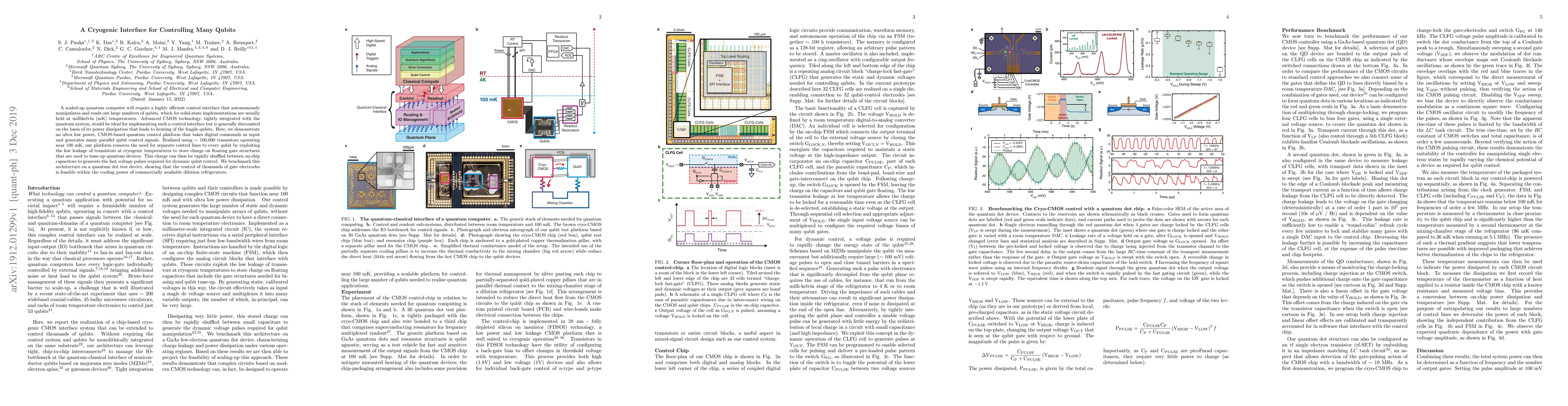
A scaled-up quantum computer will require a highly efficient control interface that autonomously manipulates and reads out large numbers of qubits, which for solid-state implementations are usually ...
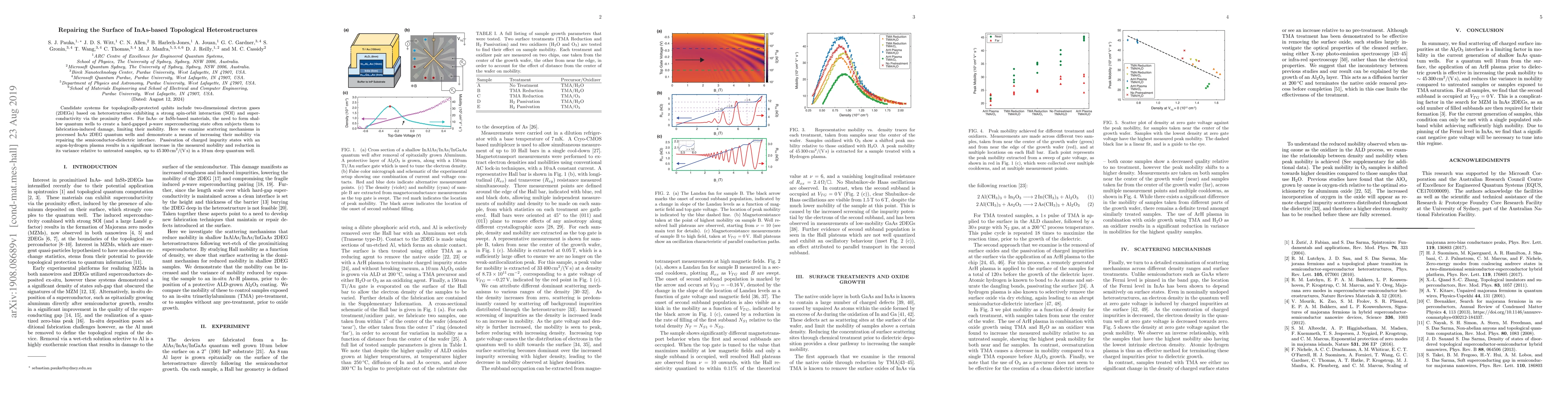
Candidate systems for topologically-protected qubits include two-dimensional electron gases (2DEGs) based on heterostructures exhibiting a strong spin-orbit interaction (SOI) and superconductivity v...
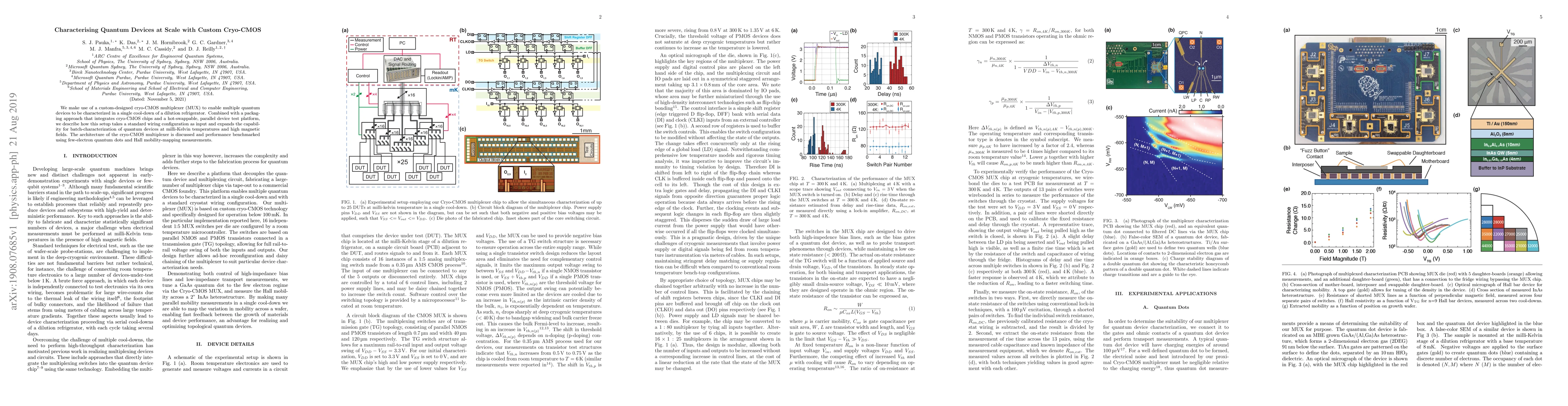
We make use of a custom-designed cryo-CMOS multiplexer (MUX) to enable multiple quantum devices to be characterized in a single cool-down of a dilution refrigerator. Combined with a packaging approa...
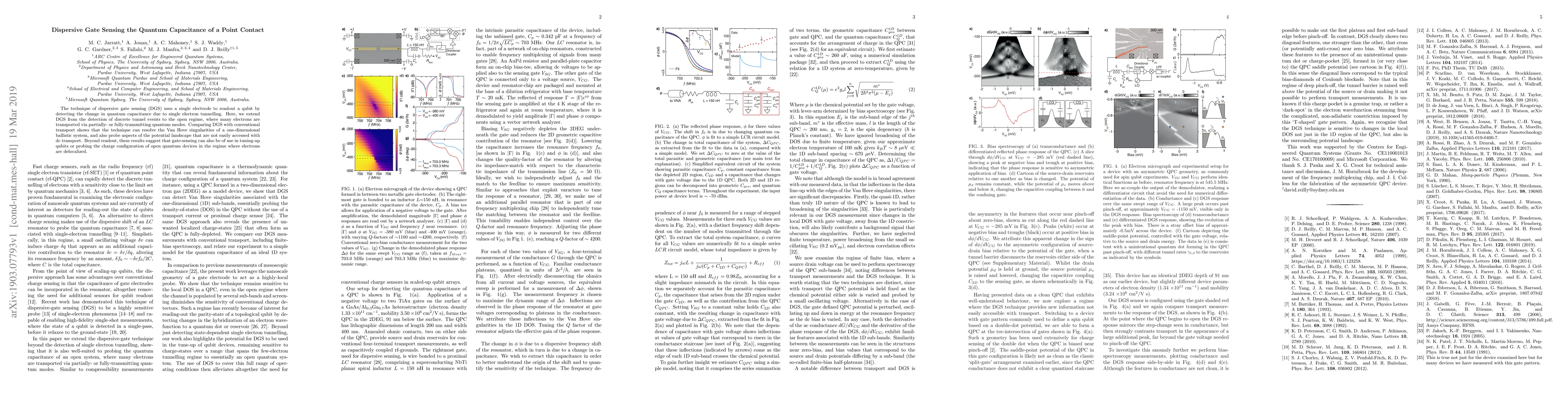
The technique of dispersive gate sensing (DGS) uses a single electrode to readout a qubit by detecting the change in quantum capacitance due to single electron tunnelling. Here, we extend DGS from t...
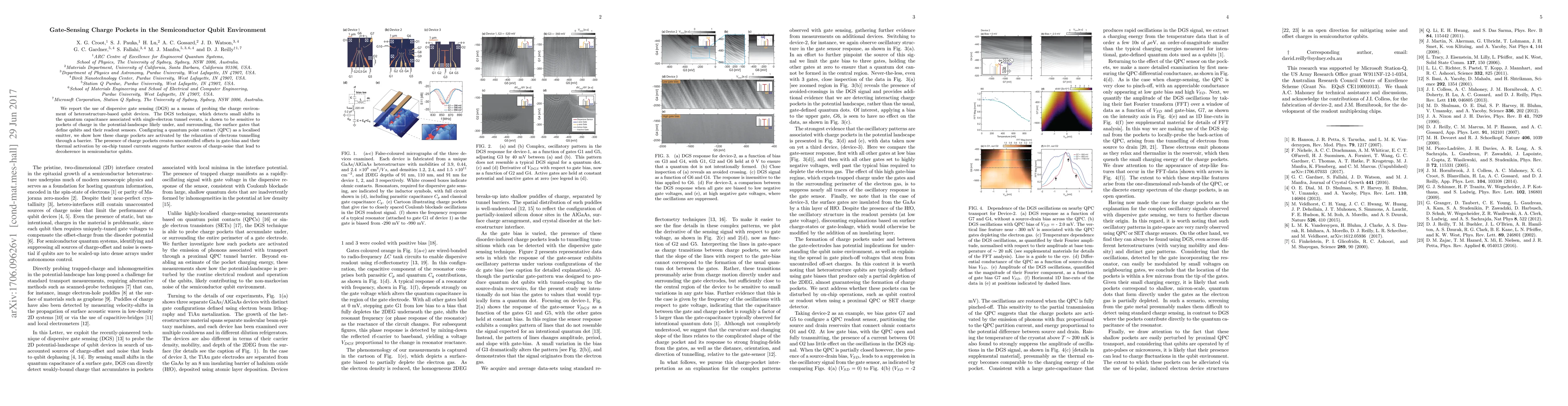
We report the use of dispersive gate sensing (DGS) as a means of probing the charge environment of heterostructure-based qubit devices. The DGS technique, which detects small shifts in the quantum c...