ArxivLens
G
Researcher

Genevieve Clark

14 papers on arXiv

14 arXiv Papers
7 Total Publications
Profile

Academic Profile

Name Genevieve H. Clark
Total Papers 7
Scholar Profile View on Semantic Scholar
Metrics

Statistics

14 arXiv Papers
7 Total Publications
Publications

Papers on arXiv

Thumbnail for A piezoelectric ski-jump laser beam scanning chip-to-free space photonic
  link
arXiv
A piezoelectric ski-jump laser beam scanning chip-to-free space photonic link

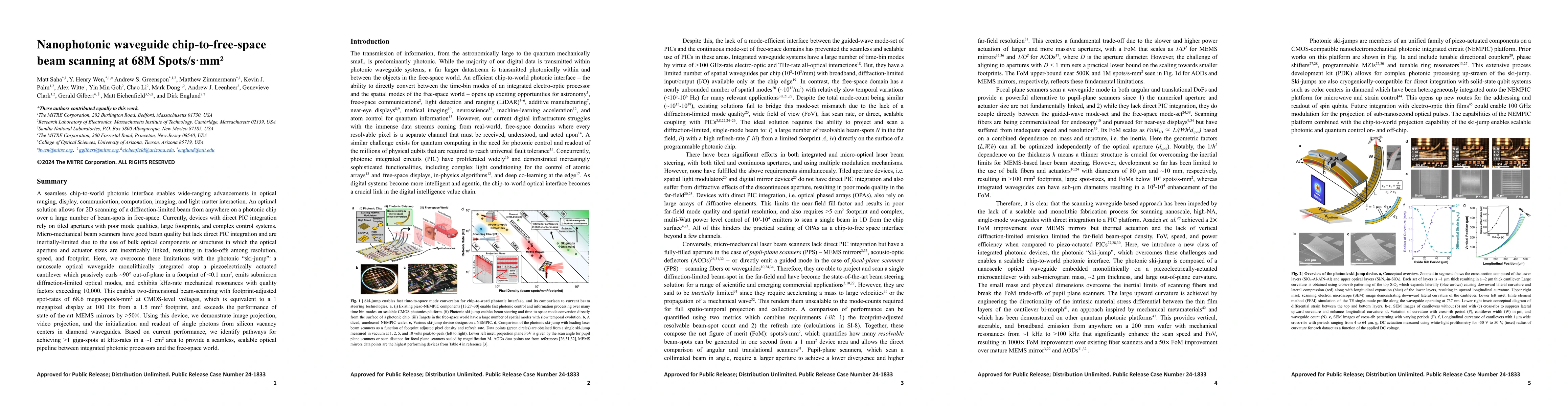
A seamless interface between integrated photonic processors and targets in free-space enables wide-ranging advancements in telescopy, free-space communication, optical ranging, materials processing,...

Thumbnail for Heterogeneous integration of spin-photon interfaces with a scalable CMOS
  platform
arXiv
Heterogeneous integration of spin-photon interfaces with a scalable CMOS platform

Color centers in diamonds have emerged as a leading solid-state platform for advancing quantum technologies, satisfying the DiVincenzo criteria and recently achieving a quantum advantage in secret k...

Thumbnail for Nanoelectromechanical control of spin-photon interfaces in a hybrid
  quantum system on chip
arXiv
Nanoelectromechanical control of spin-photon interfaces in a hybrid quantum system on chip

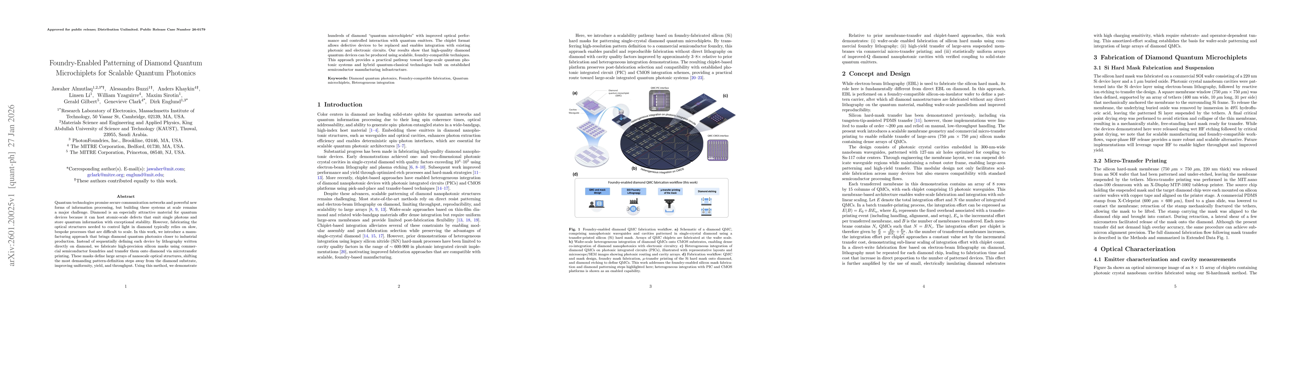
Atom-like defects or color centers (CC's) in nanostructured diamond are a leading platform for optically linked quantum technologies, with recent advances including memory-enhanced quantum communica...

Thumbnail for Modular chip-integrated photonic control of artificial atoms in diamond
  nanostructures
arXiv
Modular chip-integrated photonic control of artificial atoms in diamond nanostructures

A central goal in creating long-distance quantum networks and distributed quantum computing is the development of interconnected and individually controlled qubit nodes. Atom-like emitters in diamon...

Thumbnail for Multiplexed control of spin quantum memories in a photonic circuit
arXiv
Multiplexed control of spin quantum memories in a photonic circuit

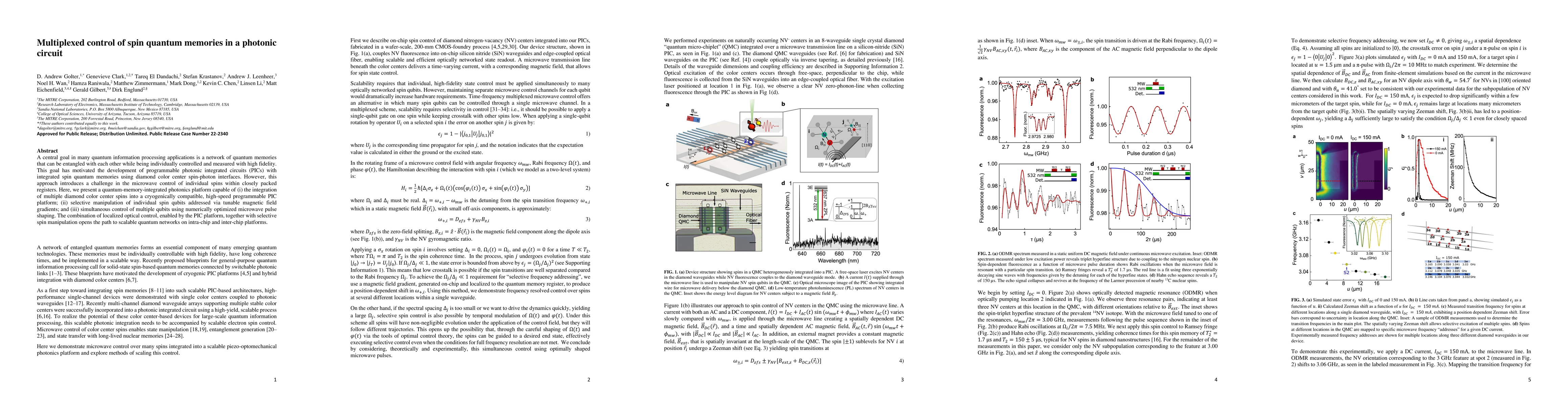
A central goal in many quantum information processing applications is a network of quantum memories that can be entangled with each other while being individually controlled and measured with high f...

Thumbnail for Programmable photonic integrated meshes for modular generation of
  optical entanglement links
arXiv
Programmable photonic integrated meshes for modular generation of optical entanglement links

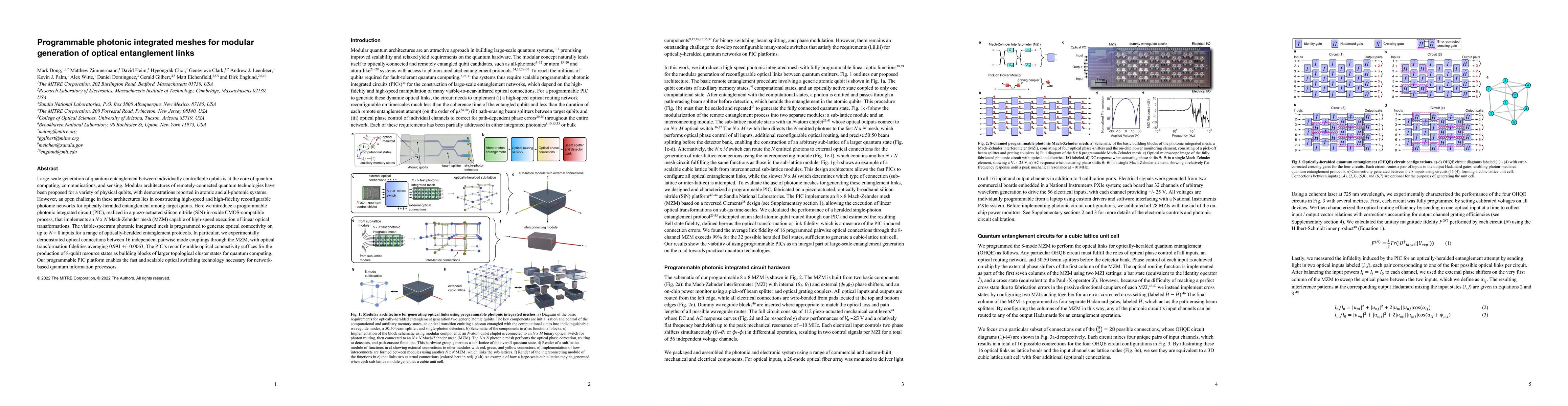
Large-scale generation of quantum entanglement between individually controllable qubits is at the core of quantum computing, communications, and sensing. Modular architectures of remotely-connected ...

Thumbnail for Piezo-optomechanical cantilever modulators for VLSI visible photonics
arXiv
Piezo-optomechanical cantilever modulators for VLSI visible photonics

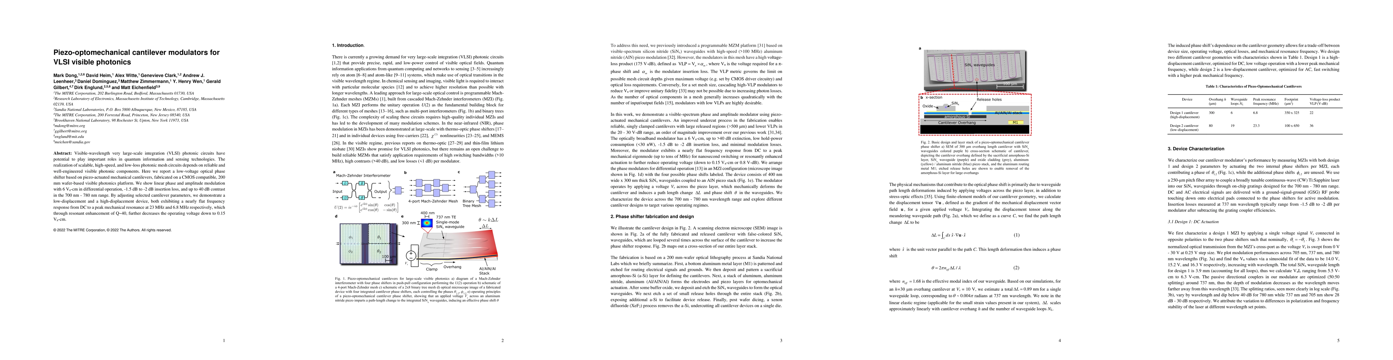
Visible-wavelength very large-scale integration (VLSI) photonic circuits have potential to play important roles in quantum information and sensing technologies. The realization of scalable, high-spe...

Thumbnail for High-speed programmable photonic circuits in a cryogenically compatible,
  visible-NIR 200 mm CMOS architecture
arXiv
High-speed programmable photonic circuits in a cryogenically compatible, visible-NIR 200 mm CMOS architecture

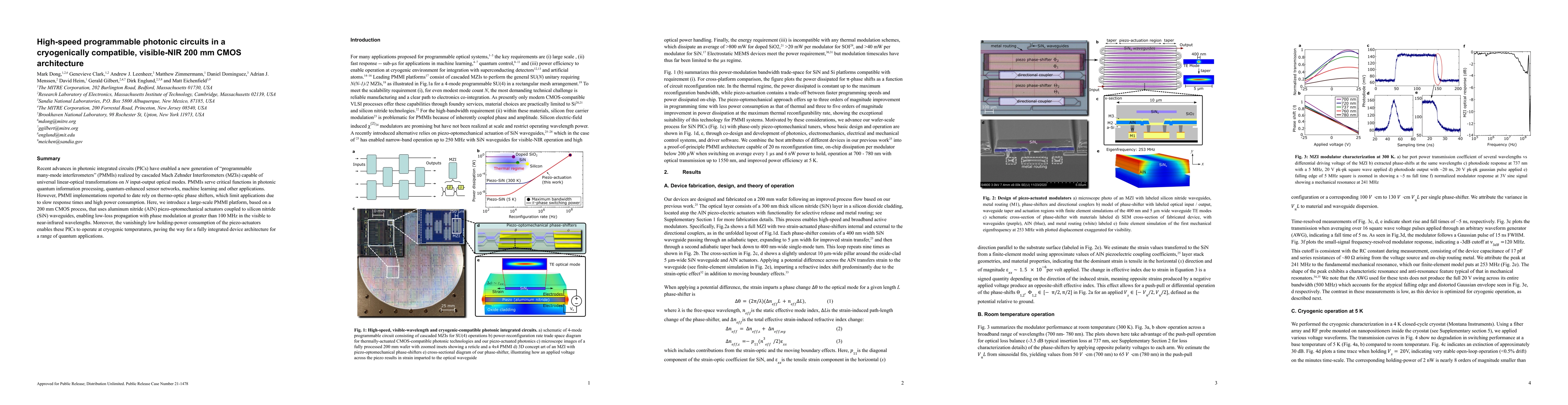
Recent advances in photonic integrated circuits (PICs) have enabled a new generation of "programmable many-mode interferometers" (PMMIs) realized by cascaded Mach Zehnder Interferometers (MZIs) capa...

Thumbnail for Cryogenic operation of silicon photonic modulators based on DC Kerr
  effect
arXiv
Cryogenic operation of silicon photonic modulators based on DC Kerr effect

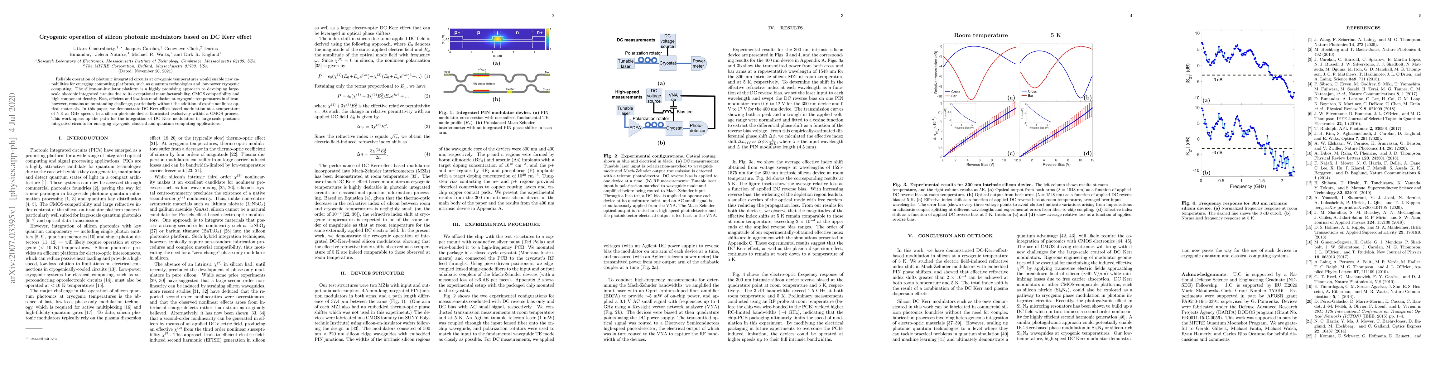
Reliable operation of photonic integrated circuits at cryogenic temperatures would enable new capabilities for emerging computing platforms, such as quantum technologies and low-power cryogenic comp...

Thumbnail for Giant and nonreciprocal second harmonic generation from layered
  antiferromagnetism in bilayer CrI3
arXiv
Giant and nonreciprocal second harmonic generation from layered antiferromagnetism in bilayer CrI3

Layered antiferromagnetism is the spatial arrangement of ferromagnetic layers with antiferromagnetic interlayer coupling. Recently, the van der Waals magnet, chromium triiodide (CrI3), emerged as th...

Thumbnail for Atomically Thin CrCl3: An in-Plane Layered Antiferromagnetic Insulator
arXiv
Atomically Thin CrCl3: An in-Plane Layered Antiferromagnetic Insulator

The recent discovery of magnetism in atomically thin layers of van der Waals (vdW) crystals has created new opportunities for exploring magnetic phenomena in the two-dimensional (2D) limit. In most ...

Thumbnail for Anisotropic structural dynamics of monolayer crystals revealed by
  femtosecond surface x-ray scattering
arXiv
Anisotropic structural dynamics of monolayer crystals revealed by femtosecond surface x-ray scattering

X-ray scattering is one of the primary tools to determine crystallographic configuration with atomic accuracy. However, the measurement of ultrafast structural dynamics in monolayer crystals remains...

Thumbnail for Scalable low loss cryogenic packaging of quantum memories in
  CMOS-foundry processed photonic chips
arXiv
Scalable low loss cryogenic packaging of quantum memories in CMOS-foundry processed photonic chips

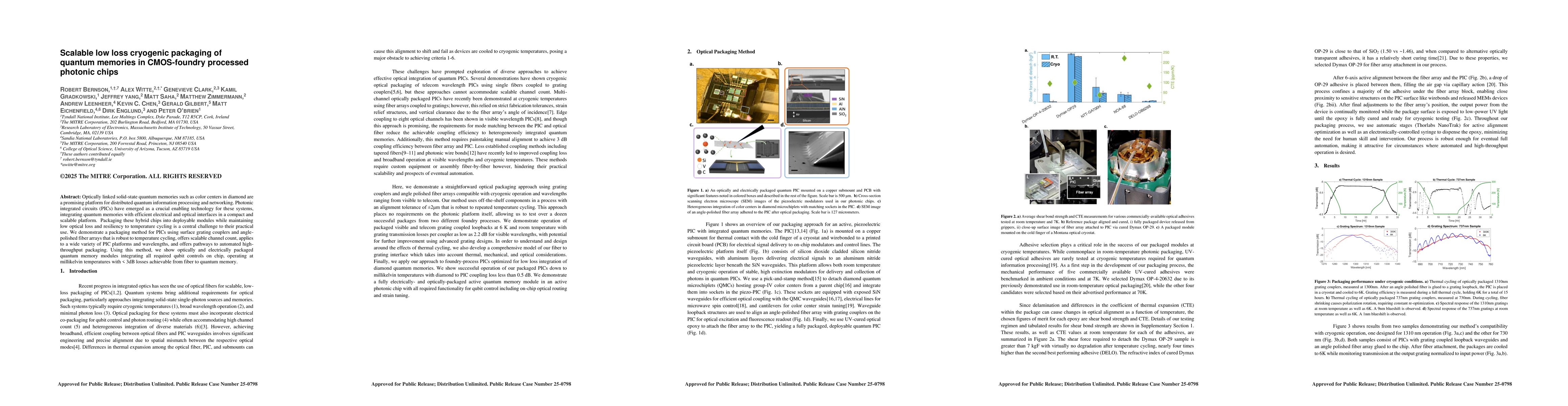
Optically linked solid-state quantum memories such as color centers in diamond are a promising platform for distributed quantum information processing and networking. Photonic integrated circuits (PIC...

Thumbnail for Foundry-Enabled Patterning of Diamond Quantum Microchiplets for Scalable Quantum Photonics
arXiv
Foundry-Enabled Patterning of Diamond Quantum Microchiplets for Scalable Quantum Photonics

Quantum technologies promise secure communication networks and powerful new forms of information processing, but building these systems at scale remains a major challenge. Diamond is an especially att...

This website uses cookies to ensure you get the best experience. Learn more