Academic Profile
Statistics
Similar Authors
Papers on arXiv
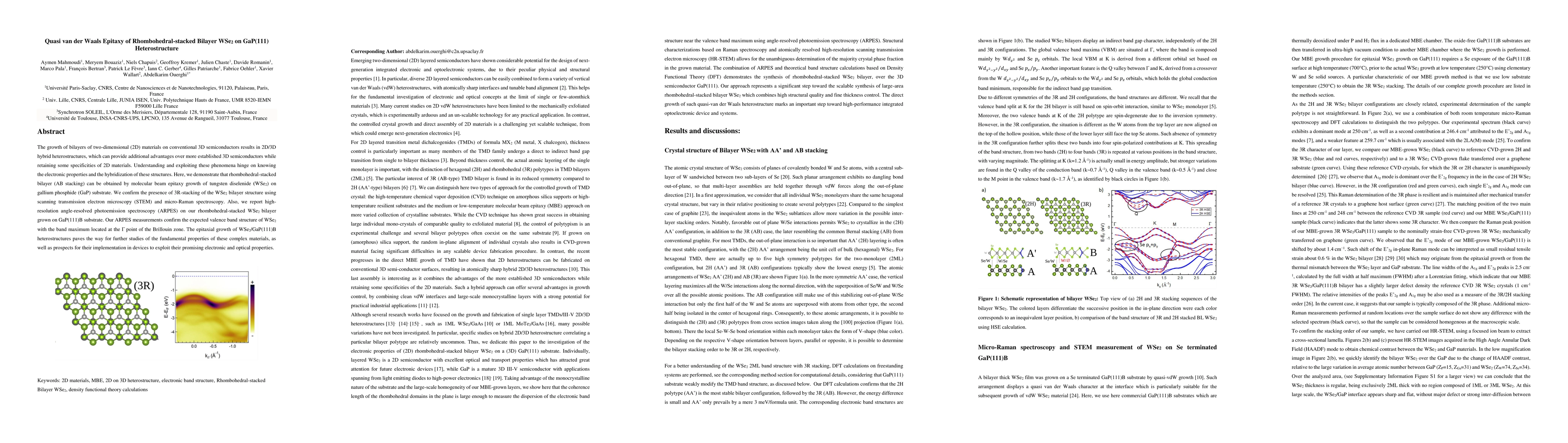
The growth of bilayers of two-dimensional (2D) materials on conventional 3D semiconductors results in 2D/3D hybrid heterostructures, which can provide additional advantages over more established 3D ...
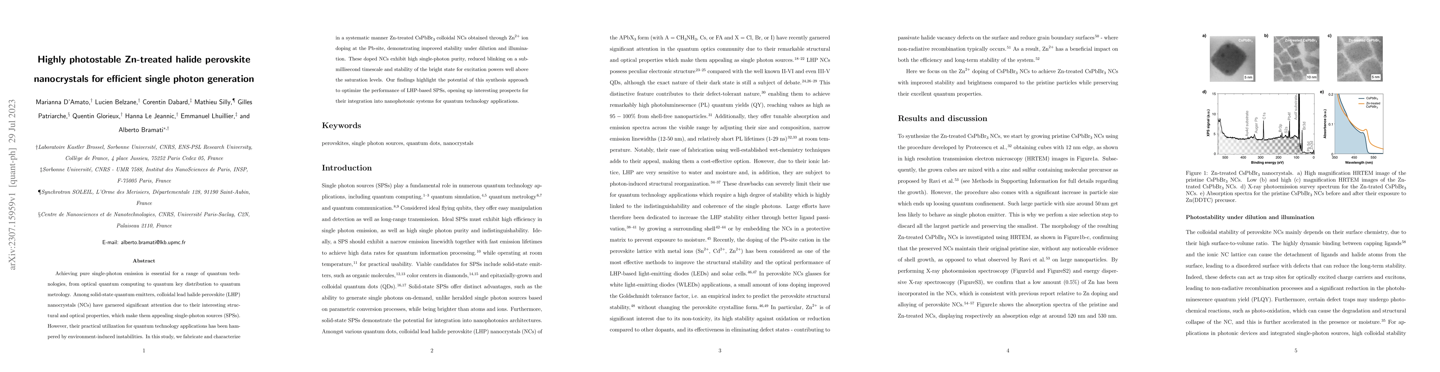
Achieving pure single-photon emission is essential for a range of quantum technologies, from optical quantum computing to quantum key distribution to quantum metrology. Among solid-state quantum emi...
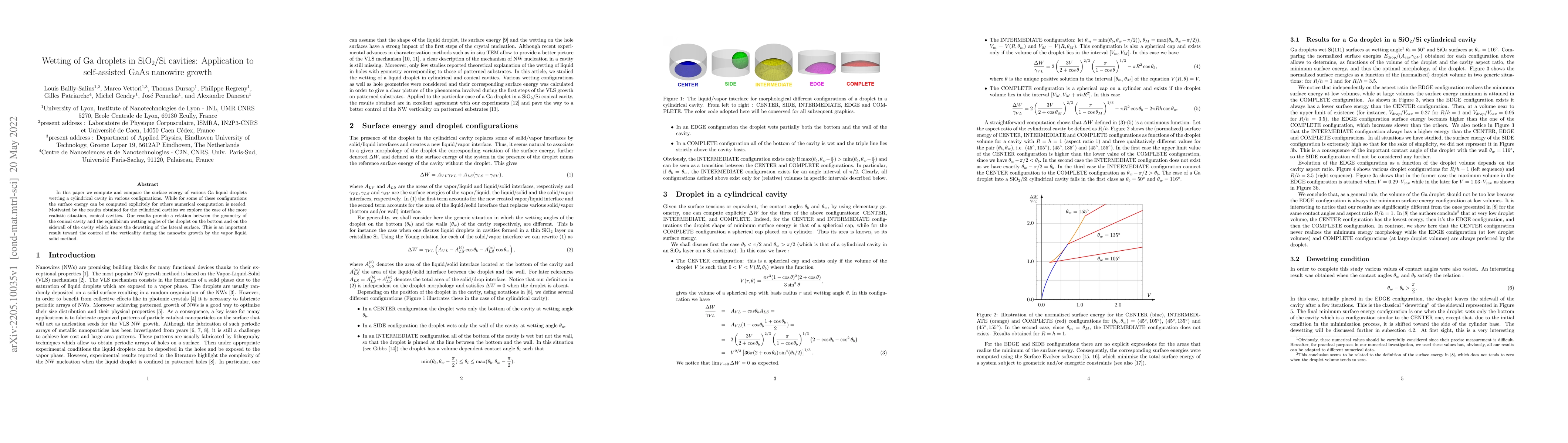
In this paper we compute and compare the surface energy of various Ga liquid droplets wetting a cylindrical cavity in various configurations. While for some of these configurations the surface energ...
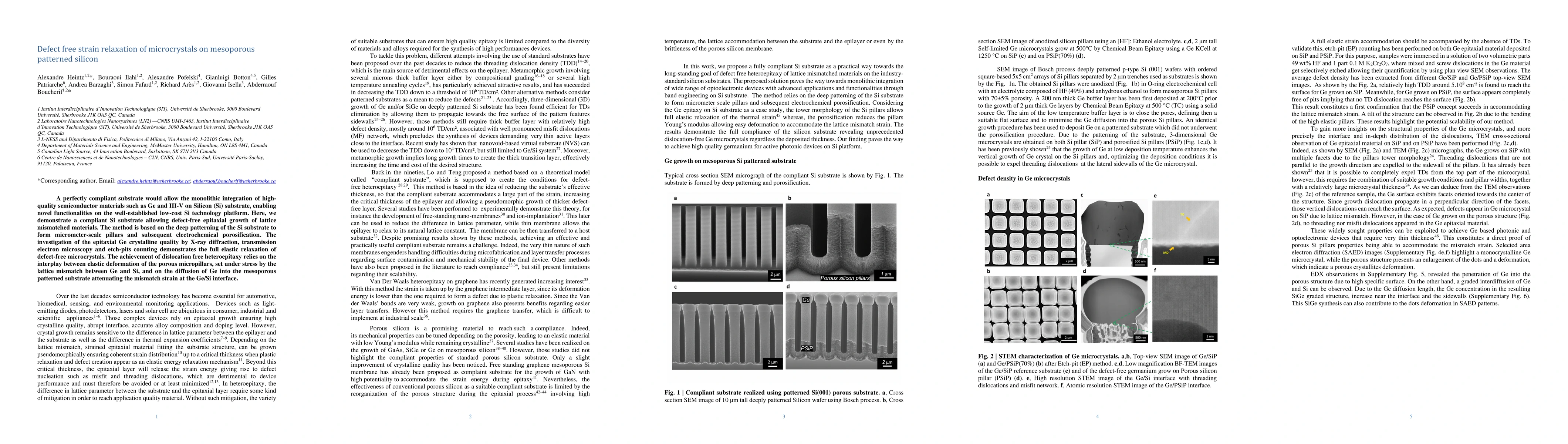
A perfectly compliant substrate would allow the monolithic integration of high-quality semiconductor materials such as Ge and III-V on Silicon (Si) substrate, enabling novel functionalities on the w...
A new process to produce Orientation-Patterned Gallium Phosphide (OP-GaP) on GaAs with almost perfectly parallel domain boundaries is presented. Taking advantage of the chemical selectivity between ...
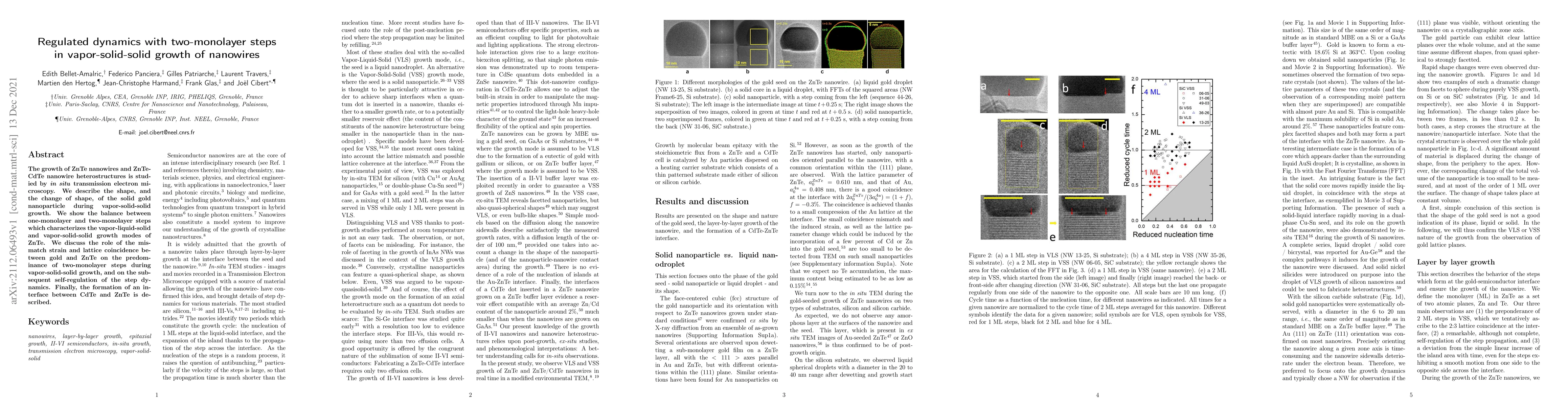
The growth of ZnTe nanowires and ZnTe-CdTe nanowire heterostructures is studied by \emph{in situ} transmission electron microscopy. We describe the shape, and the change of shape, of the solid gold ...
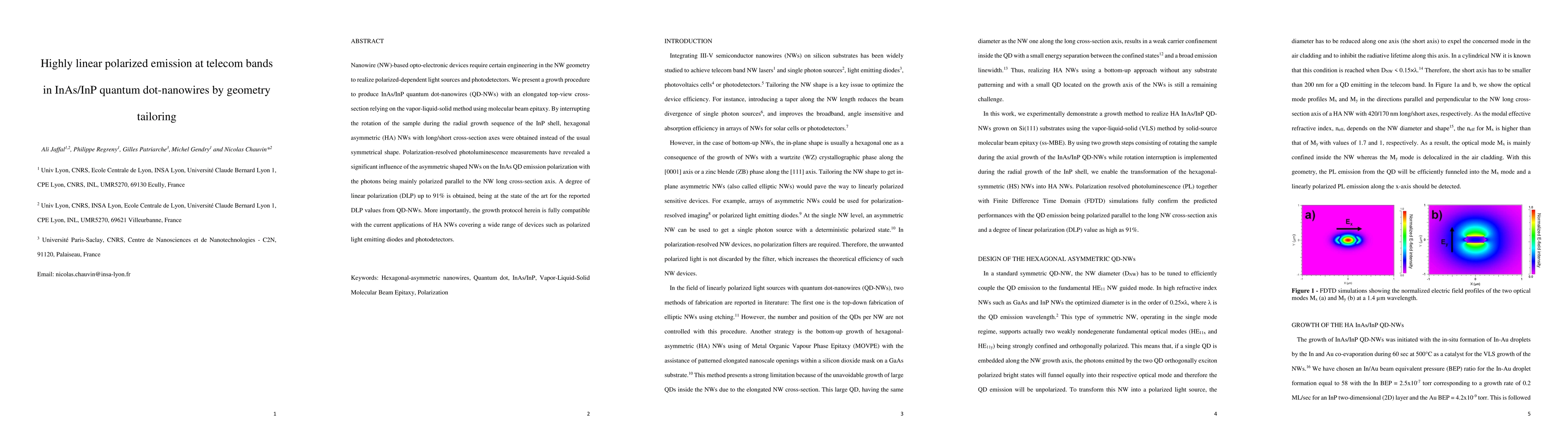
Nanowire (NW)-based opto-electronic devices require certain engineering in the NW geometry to realize polarized-dependent light sources and photodetectors. We present a growth procedure to produce I...
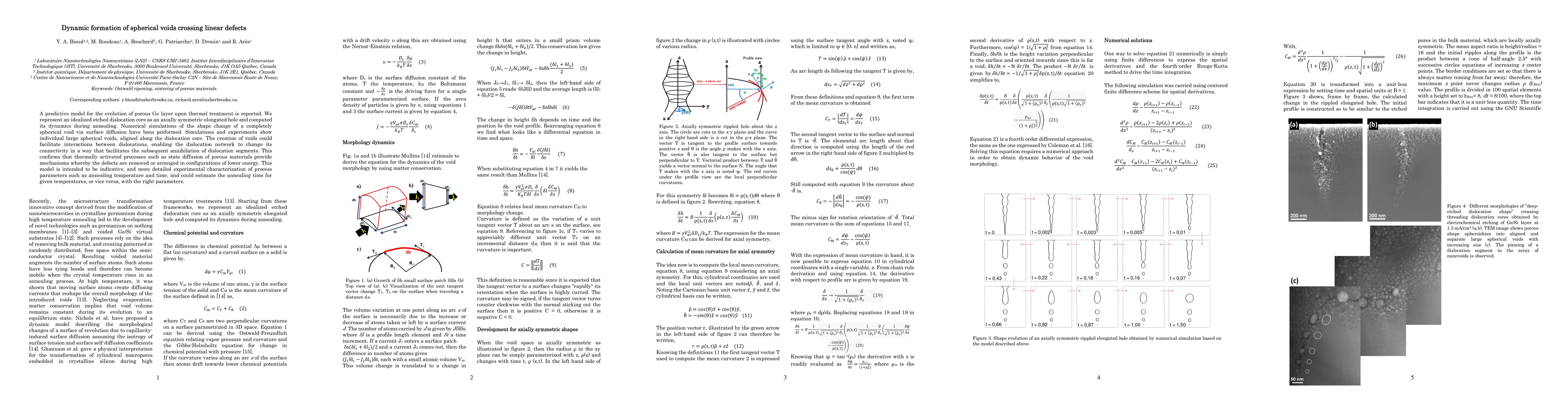
A predictive model for the evolution of porous Ge layer upon thermal treatment is reported. We represent an idealized etched dislocation core as an axially symmetric elongated hole and computed its ...
The mechanical stability of commercial GaP/Si templates during thermal an-nealing and subsequent MOCVD growth of GaP and AlGaP is investigated.Although the GaP layer of the template originally prese...
GeSn alloys are nowadays considered as the most promising materials to build Group IV laser sources on silicon (Si) in a full complementary metal oxide semiconductor-compatible approach. Recent GeSn...
Realizing high-performance nanoelectronics requires control of materials at the nanoscale. Methods to produce high quality epitaxial graphene (EG) nanostructures on silicon carbide are known. The ne...
Atomically-resolved mappings of the indium composition in InGaN/GaN multi-quantum wellstructures have been obtained by quantifying the contrast in HAADF-STEM. The quantificationprocedure presented h...
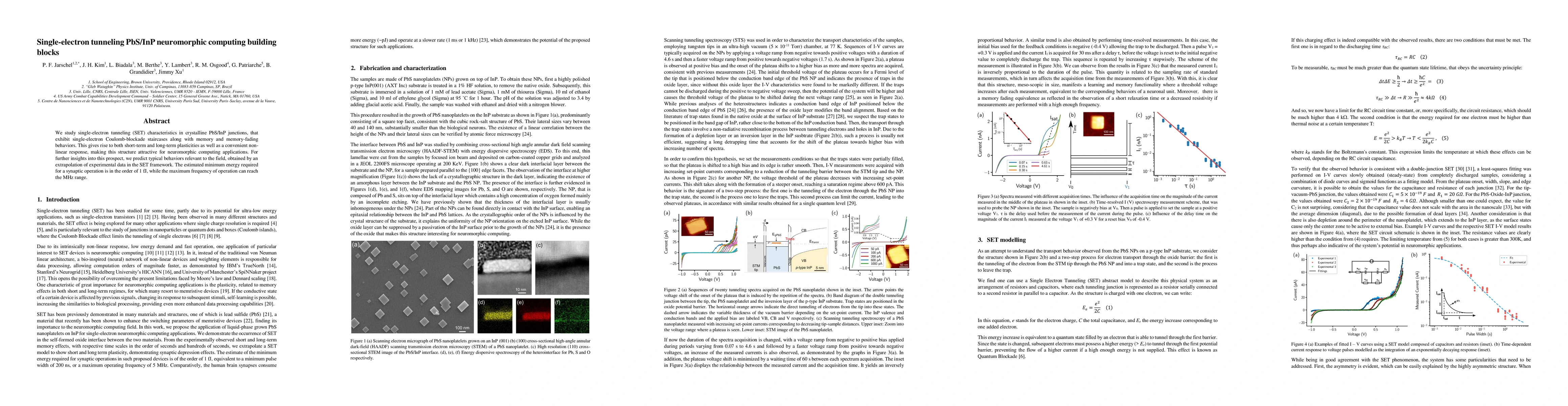
We study single-electron tunneling (SET) characteristics in crystalline PbS/InP junctions, that exhibit single-electron Coulomb-blockade staircases along with memory and memory-fading behaviors. Thi...
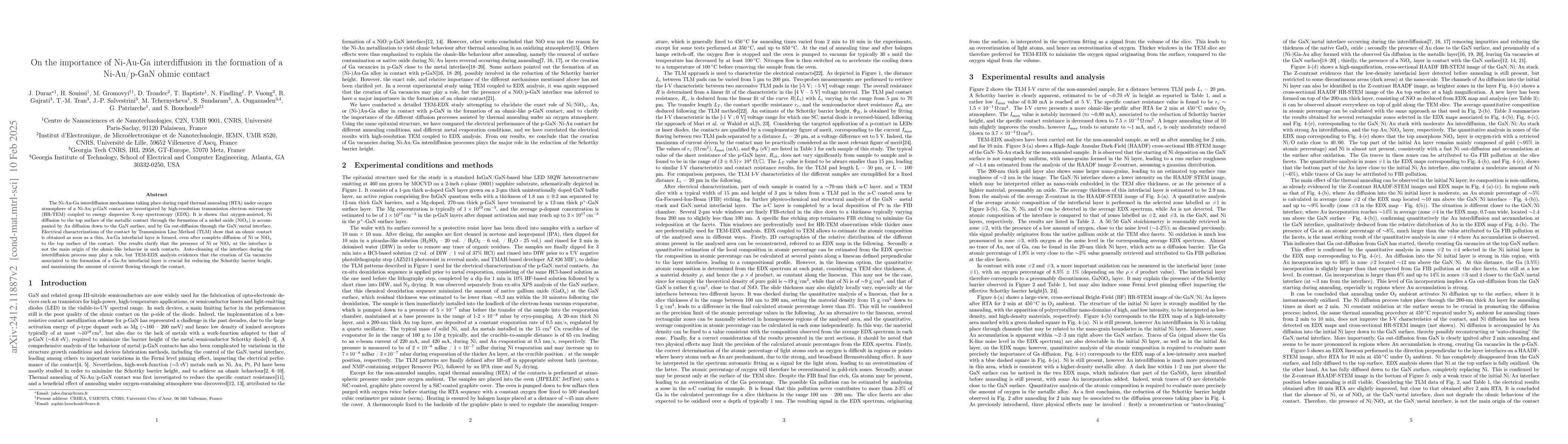
The Ni-Au-Ga interdiffusion mechanisms taking place during rapid thermal annealing (RTA) under oxygen atmosphere of a Ni-Au/p-GaN contact are investigated by high-resolution transmission electron micr...
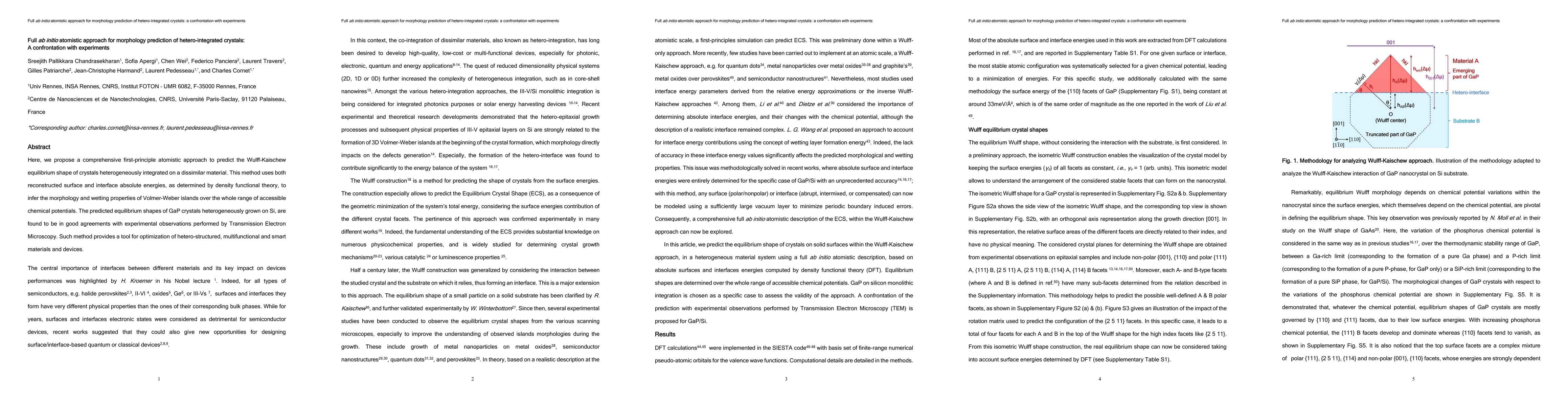
Here, we propose a comprehensive first-principle atomistic approach to predict the Wulff-Kaischew equilibrium shape of crystals heterogeneously integrated on a dissimilar material. This method uses bo...
Atomically-resolved Z-contrast and strain mappings are used to extract a model of the composition of an InGaAs/InAlAs asymmetric coupled quantum-well structure grown on InP using metal-organic vapor p...
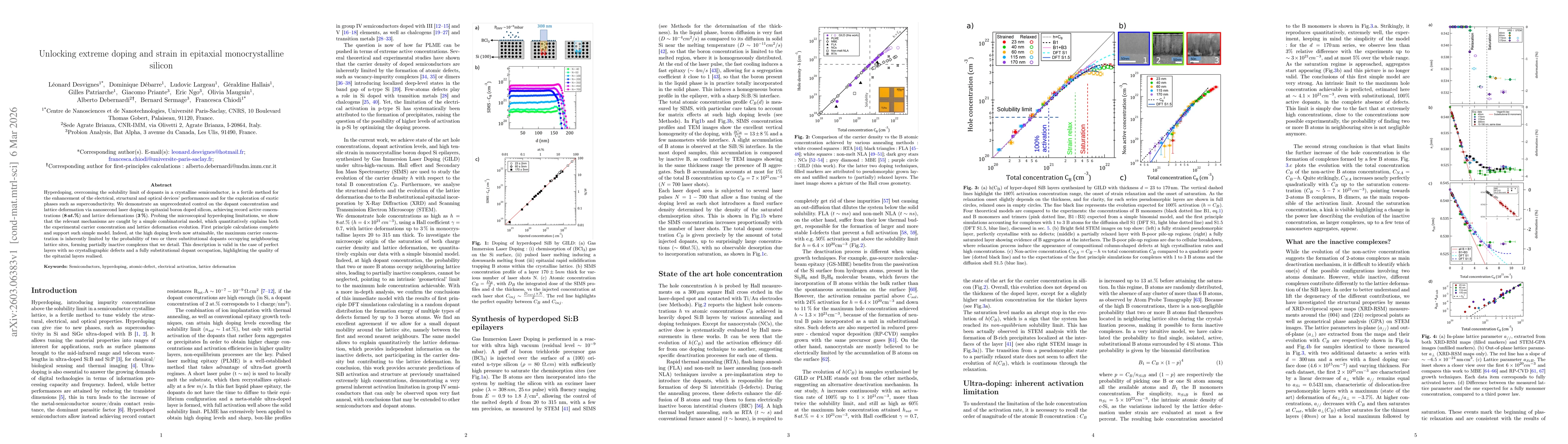
Hyperdoping, overcoming the solubility limit of dopants in a crystalline semiconductor, is a fertile method for the enhancement of the electrical, structural and optical devices' performances and for ...
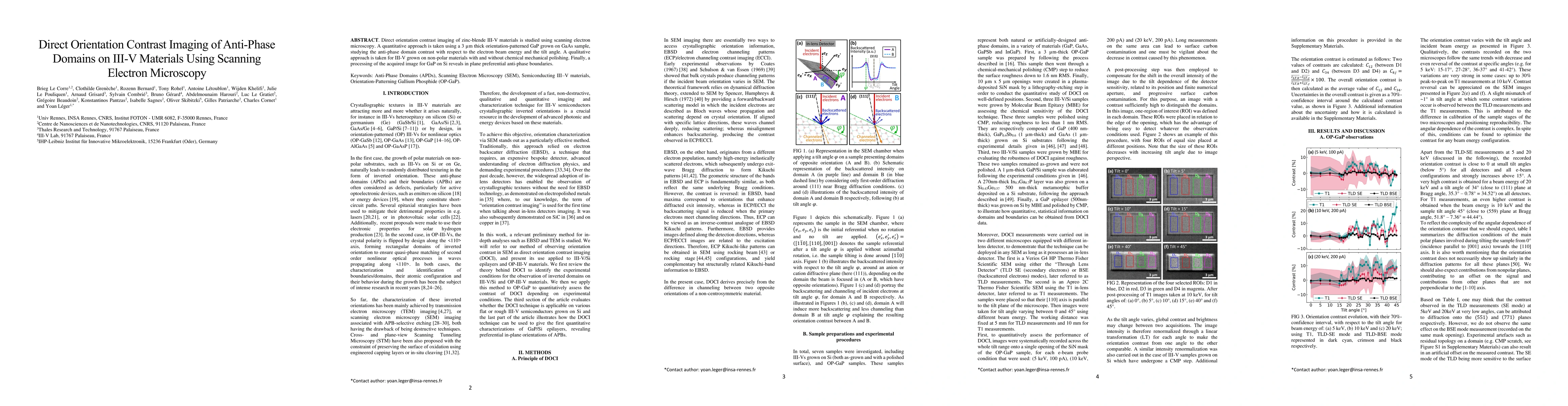
Direct orientation contrast imaging of zinc-blende III-V materials is studied using scanning electron microscopy. A quantitative approach is taken using a 3 μm thick orientation-patterned GaP grown on...